EP1103049B1 - Magnetischer speicher - Google Patents
Magnetischer speicher Download PDFInfo
- Publication number
- EP1103049B1 EP1103049B1 EP99936412A EP99936412A EP1103049B1 EP 1103049 B1 EP1103049 B1 EP 1103049B1 EP 99936412 A EP99936412 A EP 99936412A EP 99936412 A EP99936412 A EP 99936412A EP 1103049 B1 EP1103049 B1 EP 1103049B1
- Authority
- EP
- European Patent Office
- Prior art keywords
- afm
- ferromagnetic
- layer
- ferromagnetic layer
- magnetic
- Prior art date
- Legal status (The legal status is an assumption and is not a legal conclusion. Google has not performed a legal analysis and makes no representation as to the accuracy of the status listed.)
- Expired - Lifetime
Links
Images

Classifications
-
- B—PERFORMING OPERATIONS; TRANSPORTING
- B82—NANOTECHNOLOGY
- B82Y—SPECIFIC USES OR APPLICATIONS OF NANOSTRUCTURES; MEASUREMENT OR ANALYSIS OF NANOSTRUCTURES; MANUFACTURE OR TREATMENT OF NANOSTRUCTURES
- B82Y25/00—Nanomagnetism, e.g. magnetoimpedance, anisotropic magnetoresistance, giant magnetoresistance or tunneling magnetoresistance
-
- G—PHYSICS
- G11—INFORMATION STORAGE
- G11B—INFORMATION STORAGE BASED ON RELATIVE MOVEMENT BETWEEN RECORD CARRIER AND TRANSDUCER
- G11B5/00—Recording by magnetisation or demagnetisation of a record carrier; Reproducing by magnetic means; Record carriers therefor
- G11B5/74—Record carriers characterised by the form, e.g. sheet shaped to wrap around a drum
-
- G—PHYSICS
- G11—INFORMATION STORAGE
- G11B—INFORMATION STORAGE BASED ON RELATIVE MOVEMENT BETWEEN RECORD CARRIER AND TRANSDUCER
- G11B5/00—Recording by magnetisation or demagnetisation of a record carrier; Reproducing by magnetic means; Record carriers therefor
- G11B5/74—Record carriers characterised by the form, e.g. sheet shaped to wrap around a drum
- G11B5/82—Disk carriers
-
- G—PHYSICS
- G11—INFORMATION STORAGE
- G11C—STATIC STORES
- G11C11/00—Digital stores characterised by the use of particular electric or magnetic storage elements; Storage elements therefor
- G11C11/02—Digital stores characterised by the use of particular electric or magnetic storage elements; Storage elements therefor using magnetic elements
- G11C11/16—Digital stores characterised by the use of particular electric or magnetic storage elements; Storage elements therefor using magnetic elements using elements in which the storage effect is based on magnetic spin effect
- G11C11/161—Digital stores characterised by the use of particular electric or magnetic storage elements; Storage elements therefor using magnetic elements using elements in which the storage effect is based on magnetic spin effect details concerning the memory cell structure, e.g. the layers of the ferromagnetic memory cell
-
- G—PHYSICS
- G11—INFORMATION STORAGE
- G11C—STATIC STORES
- G11C11/00—Digital stores characterised by the use of particular electric or magnetic storage elements; Storage elements therefor
- G11C11/56—Digital stores characterised by the use of particular electric or magnetic storage elements; Storage elements therefor using storage elements with more than two stable states represented by steps, e.g. of voltage, current, phase, frequency
- G11C11/5607—Digital stores characterised by the use of particular electric or magnetic storage elements; Storage elements therefor using storage elements with more than two stable states represented by steps, e.g. of voltage, current, phase, frequency using magnetic storage elements
-
- H—ELECTRICITY
- H01—ELECTRIC ELEMENTS
- H01F—MAGNETS; INDUCTANCES; TRANSFORMERS; SELECTION OF MATERIALS FOR THEIR MAGNETIC PROPERTIES
- H01F10/00—Thin magnetic films, e.g. of one-domain structure
- H01F10/32—Spin-exchange-coupled multilayers, e.g. nanostructured superlattices
- H01F10/3218—Exchange coupling of magnetic films via an antiferromagnetic interface
-
- H—ELECTRICITY
- H01—ELECTRIC ELEMENTS
- H01F—MAGNETS; INDUCTANCES; TRANSFORMERS; SELECTION OF MATERIALS FOR THEIR MAGNETIC PROPERTIES
- H01F10/00—Thin magnetic films, e.g. of one-domain structure
- H01F10/32—Spin-exchange-coupled multilayers, e.g. nanostructured superlattices
- H01F10/324—Exchange coupling of magnetic film pairs via a very thin non-magnetic spacer, e.g. by exchange with conduction electrons of the spacer
- H01F10/3268—Exchange coupling of magnetic film pairs via a very thin non-magnetic spacer, e.g. by exchange with conduction electrons of the spacer the exchange coupling being asymmetric, e.g. by use of additional pinning, by using antiferromagnetic or ferromagnetic coupling interface, i.e. so-called spin-valve [SV] structure, e.g. NiFe/Cu/NiFe/FeMn
- H01F10/3272—Exchange coupling of magnetic film pairs via a very thin non-magnetic spacer, e.g. by exchange with conduction electrons of the spacer the exchange coupling being asymmetric, e.g. by use of additional pinning, by using antiferromagnetic or ferromagnetic coupling interface, i.e. so-called spin-valve [SV] structure, e.g. NiFe/Cu/NiFe/FeMn by use of anti-parallel coupled [APC] ferromagnetic layers, e.g. artificial ferrimagnets [AFI], artificial [AAF] or synthetic [SAF] anti-ferromagnets
-
- G—PHYSICS
- G11—INFORMATION STORAGE
- G11B—INFORMATION STORAGE BASED ON RELATIVE MOVEMENT BETWEEN RECORD CARRIER AND TRANSDUCER
- G11B5/00—Recording by magnetisation or demagnetisation of a record carrier; Reproducing by magnetic means; Record carriers therefor
- G11B2005/0002—Special dispositions or recording techniques
- G11B2005/0005—Arrangements, methods or circuits
-
- G—PHYSICS
- G11—INFORMATION STORAGE
- G11B—INFORMATION STORAGE BASED ON RELATIVE MOVEMENT BETWEEN RECORD CARRIER AND TRANSDUCER
- G11B5/00—Recording by magnetisation or demagnetisation of a record carrier; Reproducing by magnetic means; Record carriers therefor
- G11B5/012—Recording on, or reproducing or erasing from, magnetic disks
Definitions
- the invention relates to a magnetic memory for binary data as it previously implemented, for example, as a hard disk or removable disk has been.
- the binary data is magnetically stored on thin magnetic layers, which are magnetized in certain directions depending on the location. This results in a magnetization pattern to which columns of numbers (data) can be assigned. Due to the special design of the read or write head, however, it is only possible to apply data in the form of two magnetization directions. This assigns a zero or one (no / yes information) to each magnetized area.
- the storage density of the data carrier results from the packing density of the individual magnetic areas and is physically limited by the size of the coercive force H c of the magnetic layer [G. Bate, J. Mag. Mag. Mat. 100, pp. 413-424 (1991), W. Zinn Micromagnetism of thin storage layers, 21st volume on the JFF holiday course, Jülich (1990)].
- a magnetic memory according to the preamble of claim 1 is also known from EP-A-0 718 824.
- the invention is therefore based on the object of achieving a predeterminable increase in the coercive force H C in the corresponding magnetic layers in magnetic memories.
- the solution according to the invention is based on a new physical effect in which the coercive force H C of a ferromagnetic layer can be influenced by adjacent layers of antiferromagnetic materials which have a certain crystal orientation.
- the coercive force H C of a ferromagnetic layer can be set in a targeted manner via the thickness of the adjacent antiferromagnetic layer.
- the coercive force H C in the individual ferromagnetic layers being identically adjustable, the magnetic signal is increased. This leads to an improvement in the signal-to-noise ratio.
- the thickness of the antiferromagnetic layers can always be the same size or different in each case.
- this has several ferromagnetic layers and associated antiferromagnetic layers or layer packets made of antiferromagnetic and ferromagnetic layers, each through non-magnetic intermediate layers are magnetically isolated from one another and their magnetic signal across the thickness of each ferromagnetic Layers or over the total thickness of the ferromagnetic material in a shift package is adjustable, the individual shift packages each have different coercive fields. This is a multi-level memory realizable.
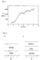
- the coercive force H C in the associated ferromagnetic layer increases with increasing thickness of the antiferromagnetic layer, which consists here, for example, of chromium.
- the antiferromagnetic layer which consists here, for example, of chromium.
- the coercive force H C in the range from 2 nm to 4 nm thickness of the antiferromagnetic layer there is a strong linear increase in the coercive force H C.
- H C coercive field strength
- FIG. 2a The basic layer structure of a magnetic memory according to the invention is shown in FIG. 2a.
- a ferromagnetic layer FM and an antiferromagnetic layer AFM are first applied to a substrate S.
- this is the simplest variant of increasing the coercive force H C in the FM layer by increasing the layer thickness of the AFM layer.
- a desired doubling of the coercive force H C can also be achieved by a layer structure according to FIG. 2b.
- an antiferromagnetic layer AFM 1 is first applied to the substrate S , which is followed by the ferromagnetic layer FM .
- a second antiferromagnetic layer AFM 2 lies over this.
- the desired increase in the coercive force H C is divided into AFM 1 + AFM 2 , ie each of the two AFM layers has to be only half as thick as the increase in H C to the same value by only one AFM layer. Since, according to the current state of knowledge, saturation of the coercive force cannot be ruled out in the case of large AFM layer thicknesses (cf. diagram, FIG. 1), this layer sequence should be preferred in order to achieve very large coercive fields.
- the basic layer structure can be multiplied, as shown in FIG. 3.
- the antiferromagnetic layers AFM i and the ferromagnetic layers FM i are then arranged X times one above the other on the substrate S.
- a structure according to FIG. 4 is suitable for realizing a multi-level memory.
- Antiferromagnetic layers AFM j , ferromagnetic layers FM j and non-magnetic insulating layers U j are arranged Y times on a substrate S one above the other.
- the layer packages each have different coercive fields.
- transition layer between the substrate S and the first AFM layer. This possibility is already indicated in FIGS. 3 and 4 by a gap between the substrate S and the first AFM layer.
- This transition layer is important for the epitaxial growth of the individual layers. Your material depends on the substrate material used.
- the substrate must be electrically neutral and can consist, for example, of Al 2 O 3 , Si, MgO or GaAs .
- it can be useful to provide a cover layer as the upper connection of the entire layer package. This serves as protection against oxidation and protection against mechanical stress.
Landscapes
- Engineering & Computer Science (AREA)
- Chemical & Material Sciences (AREA)
- Crystallography & Structural Chemistry (AREA)
- Power Engineering (AREA)
- Computer Hardware Design (AREA)
- Nanotechnology (AREA)
- Hall/Mr Elements (AREA)
- Adjustment Of Camera Lenses (AREA)
- Liquid Crystal (AREA)
- Holo Graphy (AREA)
- Mram Or Spin Memory Techniques (AREA)
Description
- Fig. 1:
- Ein Diagramm, das den Einfluß der Dicke der antiferromagnetischen Schicht auf die Höhe der Koerzitivkraft verdeutlicht,
- Fig. 2 a;b:
- Schemata des Schichtaufbaus von erfindungsgemäßen magnetischen Speichern,
- Fig. 3:
- ein Schema der Vervielfachung des Schichtaufbaus nach Fig. 2 a,
- Fig. 4:
- eine Vervielfachung einzelner Schichtenfolgen für den Aufbau von Mehrniveauspeichern,
- Fig. 5:
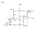
- Darstellung der Magnetisierung M zweier ferromagnetischer Schichten in Abhängigkeit vom angelegten äußeren Magnetfeld H.
MA=0.5*(M1+M2). Dies sei der Ausgangszustand.
MB=0.5*(-M1+M2).
Claims (8)
- Magnetischer Speicher für binäre Daten, mindestens aufweisend eine ferromagnetische Schicht und mindestens eine zu dieser benachbarte antiferromagnetische Schicht, die aus einem aus mehreren atomaren Monolagen bestehenden antiferromagnetischen Material besteht, und eine magnetische Wechselwirkung zwischen der antiferromagnetischen Schicht und der benachbarten ferromagnetischen Schicht (FM2, FMi) besteht
dadurch gekennzeichnet, daß
diese antiferromagnetische Schicht eine kubisch raumzentrierte Struktur und eine Kristallorientierung in (110)-Richtung aufweist, wobei die magnetischen Momente in den einzelnen Monolagen in sich antiferromagnetisch ausgerichtet sind und diese antiferromagnetische Schicht (AFM, AFMi, AFMj) eine derartige Dicke aufweist, daß die magnetische Wechselwirkung mit der benachbarten ferromagnetischen Schicht (FM, FMi, FMj), zu einer Erhöhung der Koerzitivkraft (HC) der ferromagnetischen Schicht führt, wobei über die Variation der Dicke der antiferromagnetischen Schicht (AFM, AFMi, AFMj) die Koerzitivkraft (HC) der ferromagnetischen Schicht (FM, FMi, FMj) über einen weiten Bereich gezielt einstellbar ist. - Magnetischer Speicher nach Anspruch 1,
dadurch gekennzeichnet, daß
zur Erhöhung des magnetischen Signals mehrere ferromagnetische Schichten (FMi) vorgesehen sind, zwischen denen jeweils eine antiferromagnetische Schicht (AFMi) angeordnet ist wobei die Koerzitivkraft (HC), die jeweils über die Dicke der antiferromagnetischen Schichten (AFMi) einstellbar ist, in den einzelnen ferromagnetischen Schichten (FMi) identisch ist. - Magnetischer Speicher nach Anspruch 2,
dadurch gekennzeichnet, daß
die Dicke der antiferromagnetischen Schichten (AFMi) immer gleich groß ist. - Magnetischer Speicher nach Anspruch 2,
dadurch gekennzeichnet, daß
die Dicke der antiferromagnetischen Schichten (AFMi) jeweils unterschiedlich ist. - Magnetischer Speicher nach Anspruch 1 bis 4,
dadurch gekennzeichnet, daß
dieser als Mehrniveauspeicher ausgebildet ist und mehrere ferromagnetische Schichten (FMj) und zugeordnete antiferromagnetische Schichten (AFMj) bzw. Schichtpakete aus antiferromagnetischen und ferromagnetischen Schichten aufweist, die jeweils durch unmagnetische Zwischenschichten (Uj) magnetisch voneinander isoliert sind und deren magnetisches Signal jeweils über die Dicke der einzelnen ferromagnetischen Schicht (FMj) bzw. über die Gesamtdicke des ferromagnetischen Materials in den einzelnen Schichtpaketen einstellbar ist, wobei die einzelnen Schichtpakete jeweils unterschiedliche Koerzitivfelder aufweisen. - Magnetischer Speicher nach Anspruch 1,
dadurch gekennzeichnet, daß
die Dicke (d) der antiferromagnetischen Schicht (AFM, AFMi) > 2 nm beträgt. - Magnetischer Speicher nach Anspruch 1,
dadurch gekennzeichnet, daß
die Dicke (d) der antiferromagnetischen Schicht (AFM, AFMi) vorzugsweise in einem Bereich von 2 nm < d < 12 nm liegt. - Magnetischer Speicher nach Anspruch 1,
dadurch gekennzeichnet, daß
die antiferromagnetische Schicht (AFM, AFMi, AFMj) aus einzelnen Monolagen Chrom mit einer Kristallorientierung in (110)-Richtung besteht.
Applications Claiming Priority (3)
| Application Number | Priority Date | Filing Date | Title |
|---|---|---|---|
| DE19825391 | 1998-05-28 | ||
| DE19825391A DE19825391A1 (de) | 1998-05-28 | 1998-05-28 | Magnetischer Speicher |
| PCT/DE1999/001644 WO1999062068A2 (de) | 1998-05-28 | 1999-05-28 | Magnetischer speicher |
Publications (2)
| Publication Number | Publication Date |
|---|---|
| EP1103049A2 EP1103049A2 (de) | 2001-05-30 |
| EP1103049B1 true EP1103049B1 (de) | 2003-08-27 |
Family
ID=7870172
Family Applications (1)
| Application Number | Title | Priority Date | Filing Date |
|---|---|---|---|
| EP99936412A Expired - Lifetime EP1103049B1 (de) | 1998-05-28 | 1999-05-28 | Magnetischer speicher |
Country Status (5)
| Country | Link |
|---|---|
| EP (1) | EP1103049B1 (de) |
| AT (1) | ATE248425T1 (de) |
| AU (1) | AU5152399A (de) |
| DE (2) | DE19825391A1 (de) |
| WO (1) | WO1999062068A2 (de) |
Family Cites Families (4)
| Publication number | Priority date | Publication date | Assignee | Title |
|---|---|---|---|---|
| JP2738312B2 (ja) * | 1994-09-08 | 1998-04-08 | 日本電気株式会社 | 磁気抵抗効果膜およびその製造方法 |
| US5756191A (en) * | 1994-09-13 | 1998-05-26 | Kabushiki Kaisha Toshiba | Exchange coupling film and magnetoresistance effect element |
| JPH09134510A (ja) * | 1995-11-06 | 1997-05-20 | Hitachi Metals Ltd | 磁気抵抗効果型磁気ヘッドおよびその製造方法 |
| JP3291208B2 (ja) * | 1996-10-07 | 2002-06-10 | アルプス電気株式会社 | 磁気抵抗効果型センサおよびその製造方法とそのセンサを備えた磁気ヘッド |
-
1998
- 1998-05-28 DE DE19825391A patent/DE19825391A1/de not_active Withdrawn
-
1999
- 1999-05-28 DE DE59906791T patent/DE59906791D1/de not_active Expired - Fee Related
- 1999-05-28 AU AU51523/99A patent/AU5152399A/en not_active Abandoned
- 1999-05-28 WO PCT/DE1999/001644 patent/WO1999062068A2/de not_active Ceased
- 1999-05-28 AT AT99936412T patent/ATE248425T1/de not_active IP Right Cessation
- 1999-05-28 EP EP99936412A patent/EP1103049B1/de not_active Expired - Lifetime
Also Published As
| Publication number | Publication date |
|---|---|
| DE59906791D1 (de) | 2003-10-02 |
| DE19825391A1 (de) | 1999-12-02 |
| ATE248425T1 (de) | 2003-09-15 |
| WO1999062068A2 (de) | 1999-12-02 |
| EP1103049A2 (de) | 2001-05-30 |
| AU5152399A (en) | 1999-12-13 |
| WO1999062068A3 (de) | 2000-01-13 |
Similar Documents
| Publication | Publication Date | Title |
|---|---|---|
| DE69609165T2 (de) | Nichtflüchtiger magnetoresistiver speicher mit voll geschlossenem flux-betrieb | |
| DE3882245T2 (de) | Magnetoresistiver Kopf und Verfahren zu seiner Herstellung. | |
| EP0674770B1 (de) | Magnetowiderstands-sensor mit verkürzten messschichten | |
| DE3820475C1 (de) | ||
| DE69728920T2 (de) | Kopf mit magnetoresistivem Effekt | |
| DE2442566C3 (de) | Magnetoresistiver Signalwandler | |
| DE2924013C2 (de) | ||
| DE2422927C2 (de) | Integrierte Anordnung magnetischer Wiedergabeelemente | |
| DE69204869T2 (de) | Dünnschichtmagnetkopf. | |
| DE69112940T2 (de) | Magnetische Wiedergabevorrichtung mit einem matrixartigen Netzwerk von Leseköpfen. | |
| DE19936378B4 (de) | Magnetowiderstands-Dünnschichtelement vom Spin-Valve-Typ | |
| DE2615539A1 (de) | Magnetowiderstandskopf | |
| DE3016105A1 (de) | Magnetische wandlervorrichtung zum lesen und/oder schreiben von informationen | |
| DE1960972A1 (de) | Speicheranordnung zum magnetischen Speichern einer Vielzahl von Datenbits und Verfahren zum Schreiben bzw. Lesen in bzw. aus solchen Speicheranordnungen bzw. Mehrfachbit-Mehrfachmagnetschicht-Speicherelementen solcher Speicheranordnungen | |
| DE4232244A1 (de) | Magnetowiderstands-Sensor | |
| DE1906358B2 (de) | Einrichtung fuer das aufzeichnen/abfuehlen von datensignalen an ausgewaehlten parallelspuren eines magnetischen aufzeichnungstraegers | |
| EP0442407A1 (de) | Magnetfeldsensor mit ferromagnetischer, dünner Schicht | |
| DE69124685T2 (de) | Herstellungsverfahren von magnetoresistiven Sensoren und nach diesem Verfahren hergestellte magnetische Vorrichtung | |
| DE3146932A1 (de) | "magnetoresistiver wandler zum auslesen eines aufzeichnungstraegers mit hoher informationsdichte" | |
| EP1103049A2 (de) | Magnetischer speicher | |
| DE4326999A1 (de) | Vorrichtung zum magnetfeldgesteuerten Schalten | |
| EP1155462B1 (de) | Speicherzellenanordnung und verfahren zu deren herstellung | |
| DE2124934B2 (de) | Schreibkopf zum Aufzeichnen von binären Digits auf einem sich bewegenden Magnetband in großer Dichte | |
| DE3318902C2 (de) | Verfahren zur Magnetisierung magnetisierbarer Bereiche auf einem Datenträger | |
| DE1279743B (de) | Zerstoerungsfrei ablesbare Speichervorrichtung und Verfahren zu ihrer Ansteuerung |
Legal Events
| Date | Code | Title | Description |
|---|---|---|---|
| PUAI | Public reference made under article 153(3) epc to a published international application that has entered the european phase |
Free format text: ORIGINAL CODE: 0009012 |
|
| 17P | Request for examination filed |
Effective date: 20001227 |
|
| AK | Designated contracting states |
Kind code of ref document: A2 Designated state(s): AT BE CH CY DE DK ES FI FR GB GR IE IT LI LU MC NL PT SE |
|
| 17Q | First examination report despatched |
Effective date: 20020322 |
|
| GRAH | Despatch of communication of intention to grant a patent |
Free format text: ORIGINAL CODE: EPIDOS IGRA |
|
| GRAH | Despatch of communication of intention to grant a patent |
Free format text: ORIGINAL CODE: EPIDOS IGRA |
|
| GRAA | (expected) grant |
Free format text: ORIGINAL CODE: 0009210 |
|
| AK | Designated contracting states |
Designated state(s): AT BE CH CY DE DK ES FI FR GB GR IE IT LI LU MC NL PT SE |
|
| PG25 | Lapsed in a contracting state [announced via postgrant information from national office to epo] |
Ref country code: NL Free format text: LAPSE BECAUSE OF FAILURE TO SUBMIT A TRANSLATION OF THE DESCRIPTION OR TO PAY THE FEE WITHIN THE PRESCRIBED TIME-LIMIT Effective date: 20030827 Ref country code: IT Free format text: LAPSE BECAUSE OF FAILURE TO SUBMIT A TRANSLATION OF THE DESCRIPTION OR TO PAY THE FEE WITHIN THE PRE;WARNING: LAPSES OF ITALIAN PATENTS WITH EFFECTIVE DATE BEFORE 2007 MAY HAVE OCCURRED AT ANY TIME BEFORE 2007. THE CORRECT EFFECTIVE DATE MAY BE DIFFERENT FROM THE ONE RECORDED.SCRIBED TIME-LIMIT Effective date: 20030827 Ref country code: IE Free format text: LAPSE BECAUSE OF FAILURE TO SUBMIT A TRANSLATION OF THE DESCRIPTION OR TO PAY THE FEE WITHIN THE PRESCRIBED TIME-LIMIT Effective date: 20030827 Ref country code: GB Free format text: LAPSE BECAUSE OF FAILURE TO SUBMIT A TRANSLATION OF THE DESCRIPTION OR TO PAY THE FEE WITHIN THE PRESCRIBED TIME-LIMIT Effective date: 20030827 Ref country code: FR Free format text: LAPSE BECAUSE OF FAILURE TO SUBMIT A TRANSLATION OF THE DESCRIPTION OR TO PAY THE FEE WITHIN THE PRESCRIBED TIME-LIMIT Effective date: 20030827 Ref country code: FI Free format text: LAPSE BECAUSE OF FAILURE TO SUBMIT A TRANSLATION OF THE DESCRIPTION OR TO PAY THE FEE WITHIN THE PRESCRIBED TIME-LIMIT Effective date: 20030827 Ref country code: CY Free format text: LAPSE BECAUSE OF FAILURE TO SUBMIT A TRANSLATION OF THE DESCRIPTION OR TO PAY THE FEE WITHIN THE PRESCRIBED TIME-LIMIT Effective date: 20030827 |
|
| REG | Reference to a national code |
Ref country code: GB Ref legal event code: FG4D Free format text: NOT ENGLISH |
|
| REG | Reference to a national code |
Ref country code: CH Ref legal event code: EP |
|
| REG | Reference to a national code |
Ref country code: IE Ref legal event code: FG4D Free format text: GERMAN |
|
| REF | Corresponds to: |
Ref document number: 59906791 Country of ref document: DE Date of ref document: 20031002 Kind code of ref document: P |
|
| PG25 | Lapsed in a contracting state [announced via postgrant information from national office to epo] |
Ref country code: SE Free format text: LAPSE BECAUSE OF FAILURE TO SUBMIT A TRANSLATION OF THE DESCRIPTION OR TO PAY THE FEE WITHIN THE PRESCRIBED TIME-LIMIT Effective date: 20031127 Ref country code: GR Free format text: LAPSE BECAUSE OF FAILURE TO SUBMIT A TRANSLATION OF THE DESCRIPTION OR TO PAY THE FEE WITHIN THE PRESCRIBED TIME-LIMIT Effective date: 20031127 Ref country code: DK Free format text: LAPSE BECAUSE OF FAILURE TO SUBMIT A TRANSLATION OF THE DESCRIPTION OR TO PAY THE FEE WITHIN THE PRESCRIBED TIME-LIMIT Effective date: 20031127 |
|
| PG25 | Lapsed in a contracting state [announced via postgrant information from national office to epo] |
Ref country code: ES Free format text: LAPSE BECAUSE OF FAILURE TO SUBMIT A TRANSLATION OF THE DESCRIPTION OR TO PAY THE FEE WITHIN THE PRESCRIBED TIME-LIMIT Effective date: 20031208 |
|
| PG25 | Lapsed in a contracting state [announced via postgrant information from national office to epo] |
Ref country code: PT Free format text: LAPSE BECAUSE OF FAILURE TO SUBMIT A TRANSLATION OF THE DESCRIPTION OR TO PAY THE FEE WITHIN THE PRESCRIBED TIME-LIMIT Effective date: 20040127 |
|
| NLV1 | Nl: lapsed or annulled due to failure to fulfill the requirements of art. 29p and 29m of the patents act | ||
| GBV | Gb: ep patent (uk) treated as always having been void in accordance with gb section 77(7)/1977 [no translation filed] |
Effective date: 20030827 |
|
| REG | Reference to a national code |
Ref country code: IE Ref legal event code: FD4D |
|
| PG25 | Lapsed in a contracting state [announced via postgrant information from national office to epo] |
Ref country code: LU Free format text: LAPSE BECAUSE OF NON-PAYMENT OF DUE FEES Effective date: 20040528 Ref country code: AT Free format text: LAPSE BECAUSE OF NON-PAYMENT OF DUE FEES Effective date: 20040528 |
|
| PG25 | Lapsed in a contracting state [announced via postgrant information from national office to epo] |
Ref country code: MC Free format text: LAPSE BECAUSE OF NON-PAYMENT OF DUE FEES Effective date: 20040531 Ref country code: LI Free format text: LAPSE BECAUSE OF NON-PAYMENT OF DUE FEES Effective date: 20040531 Ref country code: CH Free format text: LAPSE BECAUSE OF NON-PAYMENT OF DUE FEES Effective date: 20040531 Ref country code: BE Free format text: LAPSE BECAUSE OF NON-PAYMENT OF DUE FEES Effective date: 20040531 |
|
| PLBE | No opposition filed within time limit |
Free format text: ORIGINAL CODE: 0009261 |
|
| STAA | Information on the status of an ep patent application or granted ep patent |
Free format text: STATUS: NO OPPOSITION FILED WITHIN TIME LIMIT |
|
| 26N | No opposition filed |
Effective date: 20040528 |
|
| EN | Fr: translation not filed | ||
| BERE | Be: lapsed |
Owner name: *HAHN-MEITNER-INSTITUT BERLIN G.M.B.H. Effective date: 20040531 |
|
| REG | Reference to a national code |
Ref country code: CH Ref legal event code: PL |
|
| PGFP | Annual fee paid to national office [announced via postgrant information from national office to epo] |
Ref country code: DE Payment date: 20080516 Year of fee payment: 10 |
|
| PG25 | Lapsed in a contracting state [announced via postgrant information from national office to epo] |
Ref country code: DE Free format text: LAPSE BECAUSE OF NON-PAYMENT OF DUE FEES Effective date: 20091201 |