EP1102425A2 - Dispositif de transmission et réception optique - Google Patents
Dispositif de transmission et réception optique Download PDFInfo
- Publication number
- EP1102425A2 EP1102425A2 EP00125018A EP00125018A EP1102425A2 EP 1102425 A2 EP1102425 A2 EP 1102425A2 EP 00125018 A EP00125018 A EP 00125018A EP 00125018 A EP00125018 A EP 00125018A EP 1102425 A2 EP1102425 A2 EP 1102425A2
- Authority
- EP
- European Patent Office
- Prior art keywords
- optical
- reception apparatus
- optical transmission
- prism
- signal
- Prior art date
- Legal status (The legal status is an assumption and is not a legal conclusion. Google has not performed a legal analysis and makes no representation as to the accuracy of the status listed.)
- Withdrawn
Links
Images


Classifications
-
- H—ELECTRICITY
- H04—ELECTRIC COMMUNICATION TECHNIQUE
- H04B—TRANSMISSION
- H04B10/00—Transmission systems employing electromagnetic waves other than radio-waves, e.g. infrared, visible or ultraviolet light, or employing corpuscular radiation, e.g. quantum communication
- H04B10/25—Arrangements specific to fibre transmission
- H04B10/2589—Bidirectional transmission
Definitions
- the invention relates to an optical transmission/reception apparatus for use with uni-core bi-directional optical communication.
- optical communication for transmitting/receiving optical signals through an optical fiber.
- an optical transmissionlreception apparatus is used.
- FTTH fiber-to-the-home
- Such equipment may be enumerated by an optical fiber laid and an optical network unit (ONU) placed on the subscriber side.
- ONU optical network unit
- the ONU means an optical transmission/reception device for converting optical signals sent from the telephone station into electrical signals, or converting the electrical signals transmitted from the subscribed side into optical signals, which are transmitted to the telephone station.
- the ONU transmits/receives data through a sole optical fiber. Therefore, the ONU is in need of a light waveguide path of Y-branching for splitting the light signals into optical signals for transmission and those for reception, and a beam splitter, Moreover, in optical communication, there are occasions wherein optical signals are transmitted/received on wavelength multiplexing into two wavelengths, such as 1.3 m and 1.55 m. In such case, the ONU is in need of a wavelength selecting element, such as a wavelength filter.
- conventional ONUs are constructed using specially prepared semiconductor laser units, light receiving elements and waveguides operating as an optical path.
- the optical system of the ONU partially accounts for increased capital investment.
- the present invention provides an optical transmission/reception apparatus connected to an optical fiber operating as a communication circuit in an optical communication circuit, in which an optical signal for transmission is caused to fall on an end face of the optical fiber, with an optical signal for reception transmitted through the optical fiber to exit from an end face of the optical fiber being received by the optical transmission/reception apparatus.
- the optical transmission/reception apparatus includes light emitting means for radiating the optical signal for transmission, light beam incidence means for causing the optical signal for transmission radiated by the light emitting means to be incident on the end face of the optical fiber, and light reception means for receiving the optical signal for reception radiated from the end face of the optical fiber.
- the light beam incidence means causes a light beam of the optical signal for transmission to be incident on the optical fiber with a numerical aperture smaller than the numerical aperture of a light beam of the optical signal for reception radiated from the end face of the optical fiber.
- the light beam incidence means causes at least a portion of the wavefront of the optical signal for transmission to be coincident and overlapped with at least a portion of the wavefront of the optical signal for reception.
- a small-sized optical transmission/reception apparatus can be manufactured easily and inexpensively from simplified optical components to realize a communication network termed a fiber-to-the home.
- Fig. 1 is a block diagram showing a structure for information communication of an accessing system including an optical transmission/reception apparatus.
- Fig. 2A is a block diagram schematically showing a structure of the optical transmission/reception apparatus of Fig. 1 including a light module
- Fig. 2B is a perspective schematic view of a related art light module unit.
- Fig. 3 is a longitudinal cross-sectional view showing the structure of an optical module unit constituting the optical transmission/reception apparatus.
- Fig. 4 is a side view schematically showing the position of incidence of the optical signal for transmission to the coupling lens in the optical module unit.
- Fig. 5 is a transverse cross-sectional view showing the structure of an optical fiber of the optical transmission/reception apparatus.
- Fig. 6 is a longitudinal cross-sectional view showing the state of total reflection occurring in an optical fiber in the optical transmission/reception apparatus.
- Fig. 7 is a longitudinal cross-sectional view showing a configuration in which a light reception unit is arranged at a position immune from optical crosstalk by the reflected light beam of the optical signal for transmission produced on an end face of the optical fiber in the optical transmission/reception apparatus.
- Fig. 8 is a longitudinal cross-sectional view showing the structure provided with a light interrupting unit to prevent optical crosstalk from occurring due to the reflection light beam of the optical signal for transmission generated on an end face of the optical fiber in the optical transmission/reception apparatus.
- Fig. 9 is a side view showing a structure in which a coupling lens on the side light source of the optical transmission/reception apparatus is replaced by a concave mirror.
- Fig. 10 is a longitudinal cross-sectional view showing a structure accommodating the wavelength multiplexed communication in the optical transmission/reception apparatus.
- Fig. 11 is a longitudinal cross-sectional view showing a structure in which the tuming mirror in the optical transmission/reception apparatus shown in Fig.10 is replaced by a concave mirror.
- Fig. 12 is a longitudinal cross-sectional view showing a structure in which the turning mirror in the optical transmission/reception apparatus shown in Fig.10 is replaced by a fuming prism.
- Fig. 13 is a longitudinal cross-sectional view showing an optical system for relaying an optical signal of a given wavelength to another optical transmission/reception apparatus in case of transmission/reception of an optical signal of plural wavelengths in the optical transmission/reception apparatus according to the present invention.
- Fig. 14 is a longitudinal cross-sectional view showing a structure in which a relaying prism is mounted ahead of the turning mirror in the optical transmission/reception apparatus shown in Fig.13.
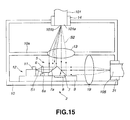
- Fig. 15 is a longitudinal cross-sectional view showing a structure not employing a turning mirror in the optical transmission/reception apparatus shown in Fig.13.
- the optical transmission/reception apparatus 1 is used in order for information equipment 201 in a household or in an office 200 to exchange information with an external network 301 via e.g., a telephone station 300, as shown in Fig.1.
- the optical transmission/reception apparatus 1, installed in the household or office 200, is connected to the telephone station 300 through an optical fiber 101, and is able to have communication with the external network 301 through the telephone station 300.
- the external network 301 is preferably a public telephone network or Internet.
- the optical transmission/reception apparatus 1 is connected over a signal line 102 to information equipment 201 in the household or office 200, and is able to distribute the information from the external network 301 to each of multiple information equipment 201 or conversely to distribute the information from each of the multiple information equipment 201 to the external network 301.
- the information equipment 201 may be, for example, a computer, a television telephone or cable television.
- the information transmitted from each of the information equipment 201 is transmitted from the optical transmission/reception apparatus 1 as an optical signal for transmission S1.
- the information sent from the external network 301 to each of the information equipment 201 is received by the optical transmission/reception apparatus 1 as an optical signal for reception S2.
- the optical transmission/reception apparatus 1 preferably includes an optical module unit 2, an electric circuit unit 3 and a voltage source unit 4, as shown in Fig.2A.
- the optical module unit 2 is made up of a light source, such as a semiconductor laser, and a lens for optically coupling the light radiated by the light source to the optical fiber 101.
- the electric circuit unit 3 performs the function of modulating a light flux emitted by the light source of the optical module unit 2 responsive to the electrical signal transmitted to the telephone station 300, and the function of amplifying the optical signal S2 from the telephone station 300 received by a light receiving element of the optical module unit 2.
- This electric circuit unit 3 and the optical module unit 2 are interconnected over a signal line 103.
- the received signal, amplified by the electric circuit unit 3, is transmitted over the signal line 102 to each of the information equipment 201 of Fig.1.
- the voltage source unit 4 furnishes power to the electric circuit unit 3.
- the voltage source unit 4 and the electric circuit unit 3 are interconnected by a voltage source line 104.
- Fig. 2B is a perspective schematic view of a related art light module unit 400.
- the related art light module unit 400 shown at Fig. 2B has a light waveguide 401.
- the architecture of the related art light module unit is formed on a silicon substrate 409.
- the laser diode emits optical transmission signals at a wavelength of 1.3 ⁇ m which travel along the waveguide 401 and out of the unit light module 400.
- Optical reception signals are received at the light module unit at wavelengths of 1.3 and 1.55 ⁇ m.
- the 1.3 ⁇ m optical reception signals are received at the photodiode 405.
- the 1.55 ⁇ m optical reception signals are filtered at the wavelength filter 407 and do not reach the photodiode 405.
- the related art light module unit 400 just described, is disadvantageously large and complex and requires a wavelength filter that extinguishes the 1.55 ⁇ m reception optical signals. Therefore, the preferred embodiment uses the advantageous optical module unit 2 schematically shown at Fig. 3 and described below.
- the optical transmission/reception apparatus 1 of the preferred embodiment features an optical module unit 2 which is configured for performing uni-core bi-directional optical communication with the telephone station 300 using the optical fiber 101, as shown in Fig.3.
- the optical module unit 2 includes package 10. Within this package 10 are enclosed a semiconductor laser 11, as a light source, a set of optical elements 5, as light flux incidence means, and a photodiode 8, as light receiving means, to constitute an optical module unit 2.
- the optical fiber 101 has one end 101a detachably fitted to the connector 14 as coupling means provided in the package 10 of the optical module unit 2.
- the connector 14 is able to position the optical fiber 101 immovably with respect to the package 10.
- One skilled in the art would understand that there are many ways to couple an optical fiber 101 to the package 10, and the optical fiber 101 may be coupled to the package 10 in any of these ways in accord with the preferred embodiment
- the semiconductor laser 11 is provided on a semiconductor element 12 mounted on a semiconductor substrate 9 secured in the package 10.
- This semiconductor laser 11 emits a laser light flux L with a wavelength of, for example, 1.3 ⁇ m.
- This laser light flux L becomes the optical signal for transmission S1 to be transmitted.
- This semiconductor laser 11 is driven by the electric circuit unit 3 within the optical transmission/reception apparatus 1.
- This electric circuit unit 3 drives the semiconductor laser 11 for generating the optical signal for transmission S1 over the signal line 103.
- This optical signal for transmission S1 has been modulated on the basis of data transmitted from information equipment 201.
- the set of one or more optical elements 5 is arranged on an optical path between the semiconductor laser 11 and the optical fiber 101.
- the set of optical elements 5 warps the optical path of the laser light flux L to cause the optical signal for transmission or optical transmission signal S1 to fall on one end of the optical fiber 101
- This set of optical elements 5 is preferably made up of a first coupling lens 6, a lens base 6a for supporting the first coupling lens 6, an optical path uplifting prism 7 and a second coupling lens 13.
- the lens base 6a supports the first coupling lens 6 for facing the semiconductor laser 11.
- the optical path uplifting prism 7 includes a reflecting surface 7a, inclined, e.g., at 45°, relative to the upper surface of the semiconductor substrate 9 and an upper surface 7b preferably parallel to the upper surface of the semiconductor substrate 9.
- This optical path uplifting prism 7 is arranged with the reflecting surface 7a directed toward the semiconductor laser 11, and has the function of reflecting the laser light flux L, beam-shaped by the first coupling lens 6, by the reflecting surface 7a to warp the optical path.
- the inclined surface 7a of the optical path uplifting prism 7, operating as the reflecting surface 7a, is provided e.g., with a total reflection film or high reflectivity coating.
- the second coupling lens 13 is disposed along the path of the laser light flux L from the semiconductor laser 11 to the optical fiber 101, while also being disposed along the optical path of the optical signal for reception or optical receiving signal S2 as radiated light from the optical fiber 101 to the photodiode 8 as light receiving means.
- This second coupling lens 13 is secured in the package 10 by a lens support 10a provided in and forming a portion of the package 10.
- the photodiode 8 receives the optical signal for reception S2 from the optical fiber 101 to convert this optical signal for reception S2 into electrical signals.
- This photodiode 8 sends the electrical signals through the signal line 103 to the electric circuit unit 3 in the optical transmission/reception apparatus 1.
- the electric circuit unit 3 amplifies the electrical signals sent from the photodiode 8 to send out the amplified signals to information equipment 201.
- the above-described semiconductor laser 11, semiconductor element 12, first coupling lens 6, lens base 6a and the optical path uplifting prism 7 are mounted on the semiconductor substrate 9.
- the photodiode 8 is preferably formed so as to be embedded in the semiconductor substrate 9.
- the center of intensity CB of the laser light flux L falls on the second coupling lens 13, with a beam diameter smaller than the light stop of the second coupling lens 13, at a position offset a distance d from the center axis CL of the second coupling lens 13. That is, this optical signal for transmission S1 falls on the optical fiber 101 with a numerical aperture smaller than that of the second coupling lens 13.
- the second coupling lens 13 is separated a distance OD from a core 101 b of the optical fiber 101. This distance OD is equal to the focal length of the second coupling lens 13. That is, the optical signal for reception S2, as light radiated by the second coupling lens 13, is collimated by the second coupling lens 13. At this time, the optical signal for reception S2 falls on the second coupling lens 13 at a numerical aperture larger than the numerical aperture of the optical signal for transmission falling on the optical fiber 101, and preferably approximately equal to that of the second coupling lens 13.
- the laser light flux L as the optical signal for transmission S1 is also a collimated light beam, and falls on the second coupling lens 13 so as to be focussed on an end face of the core 101 of the optical fiber 101.
- the set of optical elements 5 causes the light beam of the optical signal for transmission S1 to fall on the optical fiber 101 with a numerical aperture smaller than that of the light beam of the optical signal for reception S2 radiated from the end face of the optical fiber 101.
- the optical signal for transmission S1 incident from the core 101b of the optical fiber 101, is propagated through the optical fiber 101 and transmitted to the telephone station 300.
- the optical fiber 101 in general is made up of a portion termed the core 101b and a portion termed a clad 101c, as shown in Figs. 5 and 6. Since the refractive index of the core 101 b is higher than that of the clad 101c, the light through the optical fiber 101 is propagated as it undergoes repeated total reflection on the interface between the core 101b and the clad 101c.
- the diameter of the preferred core 101b is of the order of 5 ⁇ m, in case of a quartz-based optical fiber, with the diameter of the preferred clad 101c being of the order of 125 ⁇ m.
- the optical signal for reception S2 as the light radiated from the optical fiber 101,a s shown in Fig.3, is collimated by the second coupling lens 13, then falls into the inside of the optical path uplifting prism 7 from its upper surface 7b, and then exits the bottom surface of the optical path uplifting prism 7 to fall on the photodiode 8.
- the upper surface 7b of the optical path uplifting prism 7 is preferably coated with an anti-reflection film to permit the optical signal for reception S2 to be transmitted efficiently to the photodiode 8 with minimum reflection from the surface 7b.
- the center of intensity CB of the laser light flux L is offset by the distance d from the center axis CL of the second coupling lens 13, it is possible to prevent the optical signal for reception S2 from being substantially reflected by the reflecting surface 7a, and such that preferably only an outer fraction, if any, of the total collimated optical receiving signal impinges upon the surface 7a and at least the substantial fraction of the collimated optical receiving signal transmits instead through the surface 7b.
- the optical signal for reception S2 is photoelectrically converted by the photodiode 8 and transmitted to the electric circuit unit 3 through the signal line 103 of Fig.2A to complete the light transmitting/receiving operation.
- the collimated optical signal for transmission S1 is caused to fall on a portion of the second coupling lens 13 so that the optical signal for transmission S1 and the optical signal for reception S2 will be overlapped on each other on the photodiode sides of the first coupling lens 6 and the second coupling lens 13. That is, a portion of the wavefront of the optical signal for reception S2 transmitted through the second coupling lens 13 of the optical signal for reception S2 coincides with a portion of the wavefront of the optical signal for transmission S1 transmitted through the first coupling lens 6.
- a portion of the wavefront of the optical transmitting signal S1 may be coincident and overlapped with a portion of the optical receiving signal S2, or the entire optical transmitting signal S1 may be coincident and overlapped with a portion of the optical receiving signal S2.
- the wavefront herein means an equiphase plane of the electrical field of a light beam.
- the light beams may be less than fully collimated light beams.
- the two light beams are substantially collimated, wavefront coincidence can be achieved most readily.
- the optical transmission/reception apparatus 1 of the preferred embodiment can be configured to enable the so-called uni-core bi-directional optical communication.
- This uni-core bi-directional optical communication may be classified into semi-duplex optical communication and the full-duplex optical communication.
- the semi-duplex optical communication is a transmission system in which transmission is possible only in one direction at a given time point. In this sense, the semi-duplex optical communication may be compared to one-side alternate road traffic.
- the full-duplex optical communication means a transmission system in which transmission is possible in two directions simultaneously. In full-duplex optical communication, optical crosstalk, which is not problematical in the case of the semi-duplex optical communication, sometimes raises a serious problem.
- This optical crosstalk may be produced when the optical signal for transmission S1 is sent out and is reflected, e.g., on the end face of the optical fiber 101 to fall on the photodiode 8 of the optical transmissionlreception apparatus 1 as a source of transmission, as illustrated at Fig.7.
- the signal-to-noise ratio (S/N) of the optical signal for reception S2, transmitted from the telephone station, e.g., is deteriorated, such that the transmission distance by the optical fiber 101 is shortened or the data reception error is increased. Therefore, in the case of the full-duplex uni-core bi-directional optical communication, it is desired to minimize or reduce the effect of this optical crosstalk.
- the photodiode 8 is arranged so that, when the optical signal for transmission S1 is reflected by the end face of the core 101b of the optical fiber 101 and the resulting reflected light R is illuminated on the semiconductor substrate, the reflected light R is in an area offset from the area of illumination by the reflected light R, as illustrated at Fig. 7. So, in the present optical transmissionlreception apparatus 1, there is reduced risk of the laser light flux L being reflected on the end face of the core 101 b to fall on the photodiode 8, so that the optical crosstalk is reduced or minimzed by the reflected light R. Fig.
- the system 7 shows a small amount of the reflected signal S1 impinging upon the photodetector 8 which would cause a very small amount of crosstalk.
- the system may also be arranged such that no portion of the reflected signal S1 impinges upon the photodetector 8. Whether any portion of the reflected signal S1 from the end face 101b of the optical fiber 101 is incident at the photodetector 8 will depend on choices made in a balancing of a desire to have a small size and high resolution with low crosstalk.
- a beam stop or light interrupting member 15 interrupting the reflected light R, preferably which has already passed through the second coupling lens 13, to prevent a portion or substantial portion or substantially all of the reflected light R from falling on the photodiode 8 to diminish the optical crosstalk It is desired to choose a light interrupting member in this embodiment that does not block too much of the optical receiving signal S2 from reaching the photodetector 8, and thus a balancing may be performed between blocking a substantial portion of the reflected transmitting signal S1 that is reflected from the end face 101b of the optical fiber 101 and allowing the substantial portion of the optical receiving signal S2 to pass by the stop 15 and ultimately impinge upon the detector 8.
- This light interrupting member 15 may be provided not only at a position interrupting the reflected light R directly after its transmission through the second coupling lens 13 but also at a position interrupting the reflected light R prior to its incidence on the second coupling lens 13.
- the reflecting surface of the optical path uplifting prism 7 may be configured as a concave mirror 7c, as shown in Fig.9, whereby the first coupling lens 6 and the lens base 6a of the embodiment of Fig.3 may be left out or eliminated.
- the concave mirror 7c may be designed to present a cylindrically curved surface having a curvature only in one direction. The choice of a concave surface 7c or cylindrical surface 7c will depend on the choice of diode laser beam configuration. The geometry of the lens 13 may be similarly chosen accordingly.
- the optical transmission/reception apparatus 1 is demanded to receive two wavelengths, as when the optical signal for reception S2 is a so-called wavelength multiplexed optical signal for reception and comprises a light beam of a wavelength of 1.3 ⁇ m and a light beam of a wavelength of 1.55 ⁇ m, the upper surface, or surface adjacent to reflecting surface 7a, of the optical path uplifting prism 7 is preferably designed as an inclined partial reflection film 7d.
- This partial reflection film 7d is preferably designed so that it transmits a component of the collimated light beam of the receiving signal S2 with a wavelength of 1.3 ⁇ m and reflects a component of the collimated light beam of the receiving signal S2 having a wavelength of 1.55 ⁇ m.
- the 1.3 ⁇ m and 1.55 ⁇ m signals may be otherwise separated as understood by those skilled in the art, such as by using the wavelength dependent nature of the dispersive properties of the prism, or by using prism-grating ("grism") by forming a grating structure on the prism surface 7d, and corresponding placement of the two detectors 8 and 17 to detect the separated beam portions.
- grism prism-grating
- the preferred partial reflection film 7d is designed in this manner, optical signals with the wavelength of 1.3 ⁇ m are transmitted through the optical path uplifting prism 7 and received by the photodiode 8, whereas optical signal with the wavelength of 1.55 ⁇ m are reflected by the partial reflection film 7d.
- the reflected 1.55 ⁇ m component may be again reflected by a turning mirror 16 so as to be received by another photodiode 17.
- the turning mirror 16 is preferably a total reflection mirror.
- the turning mirror 16 may also serve at least a partial function as a beam stop or light interrupting means 15, such as that described above with respect to Fig. 8
- the turning mirror 16 may also be designed as a concave mirror 16a, as shown in Fig. 11. If the concave mirror 16a is used as a turning mirror, the light beam reflected by the concave mirror 16a is converged, thus enabling the beam diameter of the light beam incident on the photodiode 17 to be diminished. Thus, in this embodiment, the photodiode 17 may be reduced in size A converging lens also be placed in the beam path of the reflected 1.55 ⁇ m component of the receiving signal S2 to converge the beam prior to being incident on the detector 8.
- a turning prism 7e may be provided on the photodiode 17, in adjacency to the optical path uplifting prism 7, in place of the tuming mirror 16.
- the turning prism 7e would preferably include a mirror portion 7f on which falls the optical signal reflected by the partial reflection film 7d and which reflects the optical signal in its substantial entirety for incidence on the photodiode 17.
- the optical path uplifting prism 7 and the turning prism 7e are previously bonded to each other and are bonded together on the semiconductor substrate 9, only one bonding step to the semiconductor substrate 9 suffices. In this case, the steps of adjustment and bonding may be simpler than in the configuration employing the turning mirror 16 or 16a (or the converging lens), thus improving efficiency in the manufacturing operation.
- this optical transmission/reception apparatus 1 is used as an ONU, there are occasions where it is desired to relay the optical signal with the wavelength of 1.55 ⁇ m to another optical transmission/reception apparatus.
- an optical fiber 105 for relaying an optical signal with the wavelength of 1.55 ⁇ m may be connected to the package 10, as shown in Fig.13.
- the optical fiber 105 may alternatively be coupled to the side of the package 10 such that the turning prism 1 B is not used.
- the optical signal for reception S2 When the optical signal for reception S2, radiated by the optical fiber 101, is transmitted through the second coupling lens 13, the light component of the optical signal for reception S2, having the wavelength of 1.55 ⁇ m, is reflected by the partial reflection film 7d.
- the optical signal, reflected by the partial reflection film 7d, is reflected by the turning mirror 18 to fall on the coupling lens for relaying 19.
- a relaying prism 20 is provided between the optical path uplifting prism 7 and the turning mirror 18, as shown in Fig.20, the optical path uplifting prism 7, relaying prism 20 and the turning mirror 18 can be unified together. In this case, the adjustment and attachment in separate manufacturing steps on the semiconductor substrate 9 of the fuming mirror 18 and prism 7 are unnecessary to facilitate the manufacturing operations, thereby reducing of manufacturing cost
- the optical signal, reflected by the partial reflection film 7d, may be caused to fall directly on the coupling lens 19 for relaying and then on the optical fiber 105 for relaying, without employing the relaying prism 20 nor the turning mirror 18, as shown in Fig.15.
- This optical fiber 105 for relaying has its distal end portion detachably mounted on the package 10 through a connector 21.
- an anti-reflection film is desirably deposited for these light beams of plural wavelengths. Moreover, an anti-reflection film for the light beam with the wavelength of 1.55 ⁇ m may be deposited on the coupling lens for relaying 19.
- the signal light is assumed to have wavelengths of 1.3 pm and 1.55 ⁇ m.
- optical signals of any other suitable wavelengths may be used with the preferred embodiment
- the optical transmission/reception apparatus 1 is preferably used as an ONU for household use.
- the optical transmission/reception apparatus 1 according to the preferred embodiment may also be applied to a communication system for exchanging a variety of pieces of the information in a moving system, such as a car, an airplane or in a vessel, thus without being limited to the ONU for household use.
- the optical transmission/reception apparatus 1 is connected to an optical fiber operating as a communication circuit in an optical communication circuit, in which an optical signal for transmission S1 is caused to fall on an end face 101 b of the optical fiber 101. With an optical signal for reception S2, transmitted through the optical fiber 101 to exit from the end face 101b of the optical fiber 101, being received by the optical transmission/reception apparatus 1.
- the optical transmissionlreception apparatus 1 includes a light source 11 from which the optical transmitting signal S1 is received, or light radiating or emitting means for radiating the optical signal for transmission S1.
- the light source may be another optical fiber such as the optical fiber 105 described above which transmits a signal from another apparatus 1.
- the apparatus 1 further includes a prism or light beam incidence means 7 for causing the optical signal for transmission radiated by the light source or light emitting or radiating means to be incident on the end face 101b of the optical fiber 101, and a photodetector or light reception means 8 for receiving the optical signal for reception S2 radiated from the end face 101b of the optical fiber 101.
- the light beam incidence means 7 causes a light beam of the optical signal for transmission S1 to be incident on the optical fiber 101 with a numerical aperture smaller than the numerical aperture of a light beam of the optical signal for reception S2 radiated from the end face 101b of the optical fiber.
- the light beam incidence means causes at least a portion of the wavefront of the optical signal for transmission S1 to be coincident and overlapped with at least a portion, and preferably only an outer portion, of the wavefront of the optical signal for reception S2.
- the optical system is simplified in structure to reduce the manufacturing cost.
- the present invention provides an optical transmission/reception apparatus which may be produced to a small size readily and inexpensively using simplified optical components and a simplified overall structure.
Landscapes
- Physics & Mathematics (AREA)
- Electromagnetism (AREA)
- Engineering & Computer Science (AREA)
- Computer Networks & Wireless Communication (AREA)
- Signal Processing (AREA)
- Optical Communication System (AREA)
- Optical Couplings Of Light Guides (AREA)
Applications Claiming Priority (2)
| Application Number | Priority Date | Filing Date | Title |
|---|---|---|---|
| JP32593299 | 1999-11-16 | ||
| JP32593299A JP2001141967A (ja) | 1999-11-16 | 1999-11-16 | 光送受信装置 |
Publications (1)
| Publication Number | Publication Date |
|---|---|
| EP1102425A2 true EP1102425A2 (fr) | 2001-05-23 |
Family
ID=18182217
Family Applications (1)
| Application Number | Title | Priority Date | Filing Date |
|---|---|---|---|
| EP00125018A Withdrawn EP1102425A2 (fr) | 1999-11-16 | 2000-11-16 | Dispositif de transmission et réception optique |
Country Status (3)
| Country | Link |
|---|---|
| EP (1) | EP1102425A2 (fr) |
| JP (1) | JP2001141967A (fr) |
| SG (1) | SG97974A1 (fr) |
Cited By (2)
| Publication number | Priority date | Publication date | Assignee | Title |
|---|---|---|---|---|
| CN114035173A (zh) * | 2021-11-30 | 2022-02-11 | 图达通智能科技(苏州)有限公司 | 一种用于光电转换的耦合装置及激光雷达 |
| CN114325966A (zh) * | 2021-12-29 | 2022-04-12 | 中国电子科技集团公司第四十四研究所 | 一种平衡光电探测器二元阵列光纤耦合结构及制作方法 |
Families Citing this family (2)
| Publication number | Priority date | Publication date | Assignee | Title |
|---|---|---|---|---|
| JP3430088B2 (ja) | 1999-11-18 | 2003-07-28 | シャープ株式会社 | 光送受信モジュール |
| JP4886819B2 (ja) * | 2009-06-12 | 2012-02-29 | 日本電信電話株式会社 | 3波長多重光送受信モジュール |
Family Cites Families (2)
| Publication number | Priority date | Publication date | Assignee | Title |
|---|---|---|---|---|
| JPH10153720A (ja) * | 1996-11-25 | 1998-06-09 | Sony Corp | 光送受信装置 |
| JP3675153B2 (ja) * | 1998-02-13 | 2005-07-27 | 石川島播磨重工業株式会社 | 光学式測定装置 |
-
1999
- 1999-11-16 JP JP32593299A patent/JP2001141967A/ja not_active Withdrawn
-
2000
- 2000-11-15 SG SG200006618A patent/SG97974A1/en unknown
- 2000-11-16 EP EP00125018A patent/EP1102425A2/fr not_active Withdrawn
Cited By (3)
| Publication number | Priority date | Publication date | Assignee | Title |
|---|---|---|---|---|
| CN114035173A (zh) * | 2021-11-30 | 2022-02-11 | 图达通智能科技(苏州)有限公司 | 一种用于光电转换的耦合装置及激光雷达 |
| CN114325966A (zh) * | 2021-12-29 | 2022-04-12 | 中国电子科技集团公司第四十四研究所 | 一种平衡光电探测器二元阵列光纤耦合结构及制作方法 |
| CN114325966B (zh) * | 2021-12-29 | 2023-04-28 | 中国电子科技集团公司第四十四研究所 | 一种平衡光电探测器二元阵列光纤耦合结构及制作方法 |
Also Published As
| Publication number | Publication date |
|---|---|
| JP2001141967A (ja) | 2001-05-25 |
| SG97974A1 (en) | 2003-08-20 |
Similar Documents
| Publication | Publication Date | Title |
|---|---|---|
| US6097519A (en) | Fiber optic network using space and wavelength multiplexed data channel arrays | |
| EP0654689B1 (fr) | Module optique pour la transmission bidirectionelle | |
| US6023361A (en) | Fiber optic network using space and wavelength multiplexed data channel arrays | |
| US8540437B2 (en) | Multi-wavelength optical transmitting and receiving modules | |
| JP3782126B2 (ja) | 二方向光通信及び信号伝送用送信及び受信モジュール | |
| US5064263A (en) | Multiplexing apparatus for the direct optical reception of a plurality of optical wavelengths | |
| US7654750B2 (en) | Bidirectional optical fiber link systems component couplers | |
| US9110260B2 (en) | Hybrid optical coupling module having an alignment mark formed on an optical transmission means and an array lens and manufacturing method thereof | |
| US20050169576A1 (en) | System and method for packaging a monitor photodiode with a laser in an optical subassembly | |
| JP2000180671A5 (fr) | ||
| US6493490B1 (en) | Method and apparatus for receiving and aligning an optical communications beam with an integrated | |
| US7309169B2 (en) | Single-channel communication device for optical fibre | |
| JP6379224B2 (ja) | 多チャンネル光受信モジュールおよび多チャンネル光受信モジュールの光整列方法 | |
| CN112180521A (zh) | 一种单纤双向多通道传输光模块系统 | |
| KR100703464B1 (ko) | 양방향 광 송수신기 | |
| NL2003498C2 (nl) | Opto-elektronische inrichting voor het bidirectioneel via glasvezels transporteren van informatie en werkwijze voor het vervaardigen van een dergelijke inrichting. | |
| US20090162073A1 (en) | Optical module | |
| CN213957685U (zh) | 光收发器件 | |
| EP0153722A2 (fr) | Multiplexeur-démultiplexeur hybride optique de longueurs d'onde | |
| CN210605101U (zh) | 一种基于光波导的多路波分解复用光接收组件 | |
| JP3591932B2 (ja) | 半導体受光素子 | |
| EP1102425A2 (fr) | Dispositif de transmission et réception optique | |
| JP2004519121A (ja) | 光直列リンク | |
| CN111505775B (zh) | 光模块 | |
| US9185475B1 (en) | Signal quality in bi-directional optical links using optical circulators |
Legal Events
| Date | Code | Title | Description |
|---|---|---|---|
| PUAI | Public reference made under article 153(3) epc to a published international application that has entered the european phase |
Free format text: ORIGINAL CODE: 0009012 |
|
| AK | Designated contracting states |
Kind code of ref document: A2 Designated state(s): AT BE CH CY DE DK ES FI FR GB GR IE IT LI LU MC NL PT SE TR |
|
| AX | Request for extension of the european patent |
Free format text: AL;LT;LV;MK;RO;SI |
|
| STAA | Information on the status of an ep patent application or granted ep patent |
Free format text: STATUS: THE APPLICATION HAS BEEN WITHDRAWN |
|
| 18W | Application withdrawn |
Effective date: 20040102 |