EP1102235A1 - Voltage generator for a liquid crystal display with voltage divider, differential amplifier and switching circuit - Google Patents
Voltage generator for a liquid crystal display with voltage divider, differential amplifier and switching circuit Download PDFInfo
- Publication number
- EP1102235A1 EP1102235A1 EP00403152A EP00403152A EP1102235A1 EP 1102235 A1 EP1102235 A1 EP 1102235A1 EP 00403152 A EP00403152 A EP 00403152A EP 00403152 A EP00403152 A EP 00403152A EP 1102235 A1 EP1102235 A1 EP 1102235A1
- Authority
- EP
- European Patent Office
- Prior art keywords
- voltage
- analog
- value
- switching
- control
- Prior art date
- Legal status (The legal status is an assumption and is not a legal conclusion. Google has not performed a legal analysis and makes no representation as to the accuracy of the status listed.)
- Withdrawn
Links
Images


Classifications
-
- G—PHYSICS
- G09—EDUCATION; CRYPTOGRAPHY; DISPLAY; ADVERTISING; SEALS
- G09G—ARRANGEMENTS OR CIRCUITS FOR CONTROL OF INDICATING DEVICES USING STATIC MEANS TO PRESENT VARIABLE INFORMATION
- G09G3/00—Control arrangements or circuits, of interest only in connection with visual indicators other than cathode-ray tubes
- G09G3/20—Control arrangements or circuits, of interest only in connection with visual indicators other than cathode-ray tubes for presentation of an assembly of a number of characters, e.g. a page, by composing the assembly by combination of individual elements arranged in a matrix no fixed position being assigned to or needed to be assigned to the individual characters or partial characters
- G09G3/34—Control arrangements or circuits, of interest only in connection with visual indicators other than cathode-ray tubes for presentation of an assembly of a number of characters, e.g. a page, by composing the assembly by combination of individual elements arranged in a matrix no fixed position being assigned to or needed to be assigned to the individual characters or partial characters by control of light from an independent source
- G09G3/36—Control arrangements or circuits, of interest only in connection with visual indicators other than cathode-ray tubes for presentation of an assembly of a number of characters, e.g. a page, by composing the assembly by combination of individual elements arranged in a matrix no fixed position being assigned to or needed to be assigned to the individual characters or partial characters by control of light from an independent source using liquid crystals
- G09G3/3611—Control of matrices with row and column drivers
- G09G3/3696—Generation of voltages supplied to electrode drivers
-
- G—PHYSICS
- G09—EDUCATION; CRYPTOGRAPHY; DISPLAY; ADVERTISING; SEALS
- G09G—ARRANGEMENTS OR CIRCUITS FOR CONTROL OF INDICATING DEVICES USING STATIC MEANS TO PRESENT VARIABLE INFORMATION
- G09G2310/00—Command of the display device
- G09G2310/06—Details of flat display driving waveforms
-
- G—PHYSICS
- G09—EDUCATION; CRYPTOGRAPHY; DISPLAY; ADVERTISING; SEALS
- G09G—ARRANGEMENTS OR CIRCUITS FOR CONTROL OF INDICATING DEVICES USING STATIC MEANS TO PRESENT VARIABLE INFORMATION
- G09G2330/00—Aspects of power supply; Aspects of display protection and defect management
- G09G2330/02—Details of power systems and of start or stop of display operation
- G09G2330/021—Power management, e.g. power saving
-
- G—PHYSICS
- G09—EDUCATION; CRYPTOGRAPHY; DISPLAY; ADVERTISING; SEALS
- G09G—ARRANGEMENTS OR CIRCUITS FOR CONTROL OF INDICATING DEVICES USING STATIC MEANS TO PRESENT VARIABLE INFORMATION
- G09G3/00—Control arrangements or circuits, of interest only in connection with visual indicators other than cathode-ray tubes
- G09G3/20—Control arrangements or circuits, of interest only in connection with visual indicators other than cathode-ray tubes for presentation of an assembly of a number of characters, e.g. a page, by composing the assembly by combination of individual elements arranged in a matrix no fixed position being assigned to or needed to be assigned to the individual characters or partial characters
- G09G3/34—Control arrangements or circuits, of interest only in connection with visual indicators other than cathode-ray tubes for presentation of an assembly of a number of characters, e.g. a page, by composing the assembly by combination of individual elements arranged in a matrix no fixed position being assigned to or needed to be assigned to the individual characters or partial characters by control of light from an independent source
- G09G3/36—Control arrangements or circuits, of interest only in connection with visual indicators other than cathode-ray tubes for presentation of an assembly of a number of characters, e.g. a page, by composing the assembly by combination of individual elements arranged in a matrix no fixed position being assigned to or needed to be assigned to the individual characters or partial characters by control of light from an independent source using liquid crystals
- G09G3/3611—Control of matrices with row and column drivers
- G09G3/3685—Details of drivers for data electrodes
- G09G3/3692—Details of drivers for data electrodes suitable for passive matrices only
Definitions
- the invention relates to a device for generating an analog voltage for controlling a stable value and with low consumption, more particularly intended for controlling multi-input matrix circuits, such as crystal display screen controller circuits.
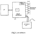
- FIG. 1 relating to art previous ordering crystal display screens liquids includes a DC controller circuit controlled by a ⁇ P microprocessor.
- This DC controller circuit includes a controller C and a charge pump allowing from a value supply voltage normalized, 5 V for example, to generate voltages of higher amplitude control, up to 9 V.
- Control voltages are delivered as rectangular voltages of given amplitude, 1.8 V, and switched between the ground voltage and the different successive levels up to the maximum voltage delivered by the charge pump, 6 levels from 0 to 9 volts per step of 1.8 volts, these rectangular level voltages different allowing in fact to adjust the level of contrast as a function of the address of the LCD segments orders.
- a solution to reduce variations of the contrast applied may consist of using at the output of the value resistance controller circuit which, by increasing the value of the current, reduce the relative variation of contrast.
- the object of the present invention is to remedy the disadvantages and limitations of controller circuits LCD display screens by the implementation of a device for generating an analog control voltage of stable value and low consumption.
- Another object of the present invention is also, thanks to the implementation of the device analog value control voltage generator stable and low consumption, the increase by a factor at least equal to 75 of the standby time embedded or portable computer systems equipped LCD liquid crystal display screens.
- Another object of the present invention is also an elimination of external capacities on the intermediate levels of the divider bridge, which allows, by integration of the latter, a reduction in the number of inputs / outputs and a reduction in the size of the chip.
- Another object of the present invention is also, due to the very low consumption of the whole, the implementation of a charge pump of reduced size, the external capacities of the pump load can be removed, a reduction corresponding to the size of the chip.
- an object of the present invention is to reduced integration costs and, because low consumption, increased autonomy and display accuracy.
- the device generating an analog control voltage of stable value and low consumption, from an analog voltage of determined nominal value, object of the invention is remarkable in that it comprises an input circuit receiving this analog voltage of determined nominal value making it possible to generate an image analog voltage of reduced value in a determined ratio k.
- a control circuit receives this analog image voltage as a set value and an image signal of the analog control voltage, image signal formed by this analog control voltage reduced in the same determined ratio k.
- This control circuit comprises at least one differential amplifier supplied by a first constant voltage of amplitude greater than the maximum value of the analog image voltage and by a second constant voltage of determined amplitude and delivers a first synchronous switching control pulse of the setpoint signal and amplitude lower than the first constant voltage and a second control pulse synchronous switching of the setpoint signal but complemented with respect to the first control pulse.
- a circuit for switching the analog control voltage, supplied by the analog voltage of determined value, is provided, this switch circuit comprising at least a first switching branch formed by an inverter / amplifier, controlled by the first switching control pulse.
- the device generating an analog voltage stable value control with low consumption, object of the invention finds application to the command of circuits based on control signals of the running type stairs, circuits such as LCD display screens by example, especially when these devices are put implemented in the form of integrated circuits in technology CMOS.
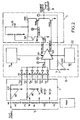
- the external resistances connected in series and denoted r 2 , r 3 , r 4 , r 5 , r 6 are shown , these resistors connected in series connecting the output of the charge pump delivering the voltage Vlcd. constituting the analog voltage of nominal value determined at the output of a pulse modulator device noted PWM, the resistors in series r 2 to r 6 thus delivering voltages V 2 , V 3 , V 4 , V 5 , V 6 , as shown in FIG. 2 and in FIG. 1, in the form of a pulse of given amplitude comprised between the value zero and a maximum value.
- the PWM pulse modulator device makes it possible to adjust the contrast applied to the liquid crystal display via the voltages V 2 to V 6 previously mentioned.
- the device which is the subject of the invention comprises an input circuit 1 receiving the analog voltage Vlcd of given nominal value, as well as of course the voltages V 5 , V 4 , V 3 , V 2 intended to accompany the analog voltage of nominal value in order to obtain the desired contrast at the abovementioned liquid crystal display.
- the input circuit 1 makes it possible to generate an analog image voltage, denoted Vjp, of reduced value in a determined ratio k.
- Vjp analog image voltage
- Vlcd of given nominal value
- V 2 , V 3 , V 4 , V 5 , V 6 is subject to the same reduction in the ratio k given previously cited.
- a set of reduced values is thus obtained, which are denoted Vj 6 , Vj 5 , Vj 4 , Vj 3 , Vj 2 , each corresponding to the voltage values V 6 , V 5 , V 4 , V 3 , V 2 respectively.
- the device which is the subject of the present invention comprises a control circuit 2 receiving the analog image voltage Vjp, that is to say Vj 2 to Vj 6 , this analog image voltage Vjp constituting in fact a set value, denoted V CONS , and an image signal Si of the analog control voltage V SEG0 , this image signal being formed by the aforementioned analog control voltage reduced in the same determined ratio k.
- the control circuit 2 comprises at least one differential amplifier 20, which in fact receives the set value V CONS and the image signal Si previously mentioned.
- the differential amplifier 20 is supplied by a first constant voltage, denoted V 21 , and by a second constant voltage, denoted V 22 , of determined amplitude.
- V 21 a first constant voltage
- V 22 a second constant voltage
- the first constant voltage V 21 is greater than the maximum value of the analog image voltage Si previously mentioned.
- the first constant voltage V 21 is a low voltage which serves as a power supply and which reduces consumption.
- the input levels of the differential amplifier 20 must be lower than that of the first supply voltage V 21 , hence the reduction by k.
- the differential amplifier 20 delivers a first switching control pulse, denoted V OUTPLUSP , this first pulse being synchronous with the reference signal V CONS and of amplitude less than the first constant voltage V 21 .
- the differential amplifier 20 also delivers a second switching control pulse, denoted V OUTMOINSP , synchronous with the reference signal V CONS but supplemented with respect to the first control pulse V OUTMOINSP .
- the device which is the subject of the invention comprises a circuit 3 for switching the analog control voltage V SEG0 .
- This circuit is supplied by the analog voltage of determined nominal value Vlcd and comprises at least a first switching branch, denoted SW 1 , formed by an inverter / amplifier, this first switching branch being controlled by the first switching control pulse V OUTPLUSP and delivering a pulse, denoted V -HI-OUT , of amplified auxiliary switching control, the latter being synchronous with the reference signal V CONS .
- the switching circuit 3 comprises a second switching branch, designated SW 2 , formed by an inverter / amplifier and controlled by the amplified auxiliary switching control pulse V -HI-OUT and by the second control pulse. switching V OUTMOINSP .
- the second switching branch SW 2 thus delivers the analog control voltage V SEG0 switched to the analog voltage of determined nominal value Vlcd.
- Figure 2 there is shown the output of the circuit 3 for switching the analog control voltage, constituting in fact the output of the device generating an analog control voltage object of the invention, connected to a capacity of the order of 170 pF to 200 pF representing the input capacity of the segments of the LCD display to be controlled.
- the input circuit 1 comprises at least one divider bridge Rj, denoted R 2 to R 6 in FIG. 2, only the divider bridges R 6 and R 5 , for reasons of simplification of the drawings, being shown in the above figure.
- Each divider bridge receives the analog voltage of nominal value Vj, that is to say V 6 , V 3 , V 2 , and delivers the analog voltage image of reduced value in the determined ratio k.
- Vj 6 , Vj 5 , Vj 4 , Vj 3 and Vj 2 the analog image voltage of reduced value is designated by Vj 6 , Vj 5 , Vj 4 , Vj 3 and Vj 2 , each of these voltages being in fact delivered by the divider bridge R 6 to R 2 corresponding.
- the input circuit 1 can include, without limitation, an analog gate Pj, in fact a set of elementary gates denoted P 1 to P 6 in FIG. 2, each analog gate Pj having a threshold value corresponding to the value of the analog image voltage of reduced value Vj 2 to Vj 6 , the corresponding analog gate delivering the analog image voltage Vjp of reduced value.
- an analog gate Pj in fact a set of elementary gates denoted P 1 to P 6 in FIG. 2, each analog gate Pj having a threshold value corresponding to the value of the analog image voltage of reduced value Vj 2 to Vj 6 , the corresponding analog gate delivering the analog image voltage Vjp of reduced value.
- control circuit 2 includes a divider bridge, denoted R CONS , this divider bridge being a bridge whose division ratio is equal to the ratio k of the determined value mentioned above.
- the aforementioned divider bridge receives the analog control voltage V SEG0 . and delivers the image signal Si of the above-mentioned analog control voltage.
- the differential amplifier 20 included in the control circuit 2 comprises a first input of a first stable reference voltage V 21 allowing the supply of the aforementioned differential amplifier.
- the first stable reference voltage V 21 is chosen at a first voltage level of determined value.
- the differential amplifier comprises a second input of a second stable reference voltage V 22 , which is chosen at a second voltage level value.
- the stable reference supply voltages V 21 and V 22 can advantageously be delivered by corresponding circuits 21 and 22, which, from a same stable reference voltage V 0 delivered by a "band gap" type circuit in Anglo-Saxon language, can deliver a first stable reference voltage at an intensity of the order of 200 ⁇ A for circuit 21, and a second stable reference voltage at an intensity of a few ⁇ A for the circuit 22.
- the reference voltage V 0 supplying the circuits 21 and 22 can be chosen to be equal to 1.25 V, for example from the aforementioned "band gap" type circuits.
- the differential amplifier 20 supplied under these conditions receives on a positive terminal Vp the image voltage Vjp delivered by the corresponding divider bridge Rj and of course by the corresponding logic gate Pj, and on its negative terminal denoted Vn the image signal Si delivered itself by the divider bridge R CONS previously mentioned in the description.
- the differential amplifier 20 delivers, on the one hand, the first control pulse switching and, secondly, the second pulse of switching control previously mentioned in the description.
- the above-mentioned circuit 3 may advantageously include a first inverter / amplifier forming the first switching branch, denoted SW 1 .
- the first amplifier inverter comprises a PMOS transistor denoted PM 1 and an NMOS transistor denoted NM 1 , these transistors being connected in cascade by their common drain / source point between the analog voltage of nominal value Vlcd and the reference voltage Vref, also designated by ground voltage.
- the gate electrode of the PMOS transistor PM 1 of the first branch receives a bias voltage equal to a fraction of the analog voltage of nominal value and the gate electrode of this transistor receives the first switching control pulse V OUTPLUSP previously mentioned in the description.
- the PMOS transistor PM 1 plays the role of a resistor, while the NMOS transistor NM 1 controlled by the first aforementioned control pulse can then play the role of an inverter switch, the common drain / source point between the aforementioned transistors delivering the amplified auxiliary switching control pulse V -HI-OUT previously mentioned in the description.
- the switching circuit 3 includes the second amplifier inverter forming the second switching branch SW 2 . It includes a PMOS transistor PM 2 and an NMOS transistor NM 2 connected in cascade by their common drain / source point between the analog voltage of determined nominal value Vlcd and the reference voltage Vref.
- the gate electrode of the PMOS transistor PM 2 receives the amplified auxiliary switching control pulse V -HI-OUT , that is to say the voltage delivered by the common drain / source point of the transistors PM 1 and NM 1 of the first branch SW 1 .
- the gate electrode of the NMOS transistor NM 2 of the second branch SW 2 receives the second switching control pulse delivered by the differential amplifier 20.
- the common drain / source point of the PMOS PM 2 transistors and NMOS NM 2 of the second branch SW 2 delivers the analog control voltage V SEG0 of stable value and with low consumption switched to the value of the analog voltage of determined nominal value Vlcd previously mentioned in the description.
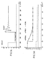
- FIG. 3b the evolution of the first control pulse V OUTPLUSP and of the second control pulse V OUTMOINSP is shown . It can be seen that the aforementioned control pulses are synchronous with the reference signal but substantially complemented, the first control pulse evolving between a low analog value substantially equal to 1 V and a high analog value less than the first constant voltage supplying the differential amplifier 20, this first constant voltage V 21 having been chosen at 2.7 V.
- the high analog voltage of the first control pulse is of the order of 2.3 V.
- the second control pulse evolves between a first high analog value substantially equal to 0.3 V and a second low analog voltage substantially equal to 0 V for the complemented parts with respect to the first control pulse.
- control pulses and in particular the difference between the signals and the respectively low and high analog values of the latter, differences substantially equal to 2.3 V, is then in a way amplified by the first switching branch circuits SW 1 and second switching branch SW 2 constituting the switching circuit 3 under the conditions below.
- the first control pulse V OUTPLUSP causes by switching of the transistor NM 1 of the first switching branch SW 1 the appearance of the amplified auxiliary control pulse V -HI-OUT by transition between the value 6.8 V and 0 V, this auxiliary control pulse being inverted with respect to the first control pulse. While the first control pulse is at the high analog value while the second control pulse is at the low analog value, the PM 2 transistor is then conductive, the junction point between the PMOS PM 2 transistor and NMOS NM 2 of the second switching branch SW 2 then being switched to the aforementioned nominal voltage analog value Vlcd.
- the voltage at test point C changes as shown in FIG. 3a with a time constant determined by the value of the load capacity of the segments of the LCD display.
- the image voltage Si changes accordingly, which makes it possible to reduce the difference at the input of the differential amplitude 20 and thus the switching at equilibrium of the first and second switching control pulses, as shown in FIG. 3b.
- the transistor PM 2 of the second switching branch SW 2 is turned off and the voltage at the test point C is then established at the load value corresponding to the analog voltage of nominal value Vlcd.
- the transient switching phenomena are represented in FIG. 3c following the switching of the PM 2 transistor previously mentioned. The segment is then charged to the nominal voltage value previously mentioned.
- the first switching control pulse V OUTPLUSP then passes in synchronism with the reference signal from a value of 1 V to the value of 0 V, whereas on the contrary the second pulse of the switching control V OUTMOINSP goes from the value 0.3 V to the maximum value 1.8 V. While the analog low level value of the first switching control pulse remains substantially equal to zero during the balancing of the voltages at the input of the differential amplifier 20, the high analog value of the second switching control pulse V OUTMOINSP decreases in a substantially regular manner until the voltages Vp and Vm are balanced at the input of the differential amplifier 20.
- the transistor PM 2 of the second switching branch SW 2 remains blocked, because it passes from a semi-blocked state close to the blocking value V T (7V) to a state blocked. It is the second control pulse V OUTMOINSP as represented in FIG. 3 which goes to 1.8 volts and therefore to a value greater than the blocking value V T (0.7 V) of the NMOS transistor NM 2 of the second switching branch. The transistor NM 2 is then conductive and the discharge of the output, as shown in FIG. 3f, is carried out.
- the initial state is then restored, the transistor NM 2 of the second switching branch SW 2 being blocked and the voltage V SEG0 having reached the new analog nominal voltage value Vlcd.
- the PM 2 transistor is used for charging and the NM 2 transistor for discharging the output.
- Figure 3g shows different transitions successively in discharge, in charge, transition amplitude of 1.8 V, then under load, transition amplitude of 3.6 V, then again in discharge, 5.4 V amplitude transition, k times the signal of instructions.
Abstract
Description
L'invention est relative à un dispositif générateur d'une tension analogique de commande de valeur stable et à faible consommation, plus particulièrement destiné à la commande de circuits matriciels multi-entrées, tels que les circuits contrôleurs d'écrans d'affichage à cristaux liquides LCD, circuits encore appelés "drivers d'écran" LCD.The invention relates to a device for generating an analog voltage for controlling a stable value and with low consumption, more particularly intended for controlling multi-input matrix circuits, such as crystal display screen controller circuits. LCD liquids, circuits also called LCD screen drivers .
En référence à la figure 1 relative à l'art antérieur, la commande d'écrans d'affichage à cristaux liquides comprend un circuit contrôleur CC piloté par un microprocesseur µP. Ce circuit contrôleur CC comporte un contrôleur proprement dit C et une pompe de charge permettant à partir d'une tension d'alimentation de valeur normalisée, 5 V par exemple, d'engendrer des tensions de commande d'amplitude supérieure, pouvant atteindre 9 V. Les tensions de commande sont délivrées sous forme de tensions rectangulaires d'amplitude donnée, 1,8 V, et commutées entre la tension de masse et les différents niveaux successifs jusqu'à la tension maximale délivrée par la pompe de charge, 6 niveaux de 0 à 9 volts par pas de 1,8 volts, ces tensions rectangulaires de niveau différent permettant en fait de régler le niveau de contraste en fonction de l'adresse des segments LCD commandés.Referring to Figure 1 relating to art previous ordering crystal display screens liquids includes a DC controller circuit controlled by a µP microprocessor. This DC controller circuit includes a controller C and a charge pump allowing from a value supply voltage normalized, 5 V for example, to generate voltages of higher amplitude control, up to 9 V. Control voltages are delivered as rectangular voltages of given amplitude, 1.8 V, and switched between the ground voltage and the different successive levels up to the maximum voltage delivered by the charge pump, 6 levels from 0 to 9 volts per step of 1.8 volts, these rectangular level voltages different allowing in fact to adjust the level of contrast as a function of the address of the LCD segments orders.
Toutefois, en raison de la capacité relativement élevée, 200 pF, des segments LCD, il est nécessaire de prévoir des capacités externes ayant pour objet de lisser les tensions finalement appliquées. Malgré l'adjonction des capacités précitées, il reste toutefois un problème de précision des niveaux de tension appliqués sur les segments LCD, avec une dégradation du contraste finalement appliqué, en particulier pour les valeurs de tension les plus hautes. Le pont diviseur est déséquilibré à partir du moment où un courant est appelé sur un des niveaux intermédiaires de ce dernier, courant permettant de charger les capacités des segments LCD.However, due to the relatively large capacity high, 200 pF, LCD segments, it is necessary to provide for external capacities intended to smooth the tensions finally applied. Despite the addition of the abovementioned capacities, there remains however a problem of accuracy of the voltage levels applied to the LCD segments, with a degradation of the contrast finally applied, especially for the voltage values the higher. The divider bridge is unbalanced from the moment when a current is called on one of the levels intermediates of the latter, current allowing load the capacities of the LCD segments.
Une solution, afin de réduire les variations relatives du contraste appliqué, peut consister à utiliser en sortie du circuit contrôleur des résistances de valeur plus faible, lesquelles, en augmentant la valeur du courant, permettent de réduire la variation relative de contraste.A solution to reduce variations of the contrast applied, may consist of using at the output of the value resistance controller circuit which, by increasing the value of the current, reduce the relative variation of contrast.
La solution précitée présente cependant l'inconvénient majeur de provoquer un appel de courant très important sur la pompe de charge, ce qui a pour effet de nécessiter d'augmenter la taille de la pompe de charge et des capacités externes.However, the above solution presents the major drawback of causing a current draw very important on the charge pump, which has the effect to increase the size of the charge pump and external capabilities.
La présente invention a pour objet de remédier aux inconvénients et limitations des circuits contrôleurs d'écrans d'affichage LCD par la mise en oeuvre d'un dispositif générateur d'une tension analogique de commande de valeur stable et à faible consommation.The object of the present invention is to remedy the disadvantages and limitations of controller circuits LCD display screens by the implementation of a device for generating an analog control voltage of stable value and low consumption.
Un autre objet de la présente invention est également, grâce à la mise en oeuvre du dispositif générateur d'une tension analogique de commande de valeur stable et à faible consommation, l'accroissement par un facteur au moins égal à 75 de l'autonomie en mode veille des systèmes informatiques embarqués ou portables équipés d'écrans d'affichage à cristaux liquides LCD. Another object of the present invention is also, thanks to the implementation of the device analog value control voltage generator stable and low consumption, the increase by a factor at least equal to 75 of the standby time embedded or portable computer systems equipped LCD liquid crystal display screens.
Un autre objet de la présente invention est également une élimination des capacités extérieures sur les niveaux intermédiaires du pont diviseur, ce qui permet, par intégration de ce dernier, une diminution du nombre d'entrées sorties et une réduction de la taille de la puce.Another object of the present invention is also an elimination of external capacities on the intermediate levels of the divider bridge, which allows, by integration of the latter, a reduction in the number of inputs / outputs and a reduction in the size of the chip.
Un autre objet de la présente invention est également, en raison de la très faible consommation de l'ensemble, la mise en oeuvre d'une pompe de charge de taille réduite, les capacités extérieures de la pompe de charge pouvant être supprimées, une réduction correspondante de la taille de la puce.Another object of the present invention is also, due to the very low consumption of the whole, the implementation of a charge pump of reduced size, the external capacities of the pump load can be removed, a reduction corresponding to the size of the chip.
Un objet de la présente invention est enfin, du fait d'une diminution des coûts d'intégration et, du fait de la faible consommation, une augmentation de l'autonomie et de la précision de l'affichage.Finally, an object of the present invention is to reduced integration costs and, because low consumption, increased autonomy and display accuracy.
Le dispositif générateur d'une tension analogique
de commande de valeur stable et à faible consommation, à
partir d'une tension analogique de valeur nominale
déterminée, objet de l'invention, est remarquable en ce
qu'il comporte un circuit d'entrée recevant cette tension
analogique de valeur nominale déterminée permettant
d'engendrer une tension analogique image de valeur réduite
dans un rapport k déterminé.
En outre, un circuit de contrôle reçoit cette tension
analogique image comme valeur de consigne et un signal
image de la tension analogique de commande, signal image
formé par cette tension analogique de commande réduite
dans le même rapport k déterminé. Ce circuit de contrôle
comprend au moins un amplificateur différentiel alimenté
par une première tension constante d'amplitude supérieure
à la valeur maximale de la tension analogique image et par
une deuxième tension constante d'amplitude déterminée et
délivre une première impulsion de contrôle de commutation
synchrone du signal de consigne et d'amplitude inférieure
à la première tension constante et une deuxième impulsion
de contrôle de commutation synchrone du signal de consigne
mais complémentée vis-à-vis de la première impulsion de
contrôle. Un circuit de commutation de la tension
analogique de commande, alimenté par la tension analogique
de valeur déterminée, est prévu, ce circuit commutateur
comportant au moins une première branche de commutation
formée par un inverseur/amplificateur, commandée par la
première impulsion de contrôle de commutation et délivrant
une impulsion de contrôle de commutation auxiliaire
amplifiée, synchrone du signal de consigne, et une
deuxième branche de commutation, formée par un
inverseur/amplificateur, commandée par l'impulsion de
contrôle de commutation auxiliaire amplifiée et par la
deuxième impulsion de contrôle de commutation et délivrant
la tension analogique de commande commutée à la tension
analogique de valeur nominale déterminée.The device generating an analog control voltage of stable value and low consumption, from an analog voltage of determined nominal value, object of the invention, is remarkable in that it comprises an input circuit receiving this analog voltage of determined nominal value making it possible to generate an image analog voltage of reduced value in a determined ratio k.
In addition, a control circuit receives this analog image voltage as a set value and an image signal of the analog control voltage, image signal formed by this analog control voltage reduced in the same determined ratio k. This control circuit comprises at least one differential amplifier supplied by a first constant voltage of amplitude greater than the maximum value of the analog image voltage and by a second constant voltage of determined amplitude and delivers a first synchronous switching control pulse of the setpoint signal and amplitude lower than the first constant voltage and a second control pulse synchronous switching of the setpoint signal but complemented with respect to the first control pulse. A circuit for switching the analog control voltage, supplied by the analog voltage of determined value, is provided, this switch circuit comprising at least a first switching branch formed by an inverter / amplifier, controlled by the first switching control pulse. and delivering an amplified auxiliary switching control pulse, synchronous with the setpoint signal, and a second switching branch, formed by an inverter / amplifier, controlled by the amplified auxiliary switching control pulse and by the second control pulse switching and delivering the switched control analog voltage to the determined nominal value analog voltage.
Le dispositif générateur d'une tension analogique de commande de valeur stable et à faible consommation, objet de l'invention, trouve application à la commande de circuits à partir de signaux de commande du type en marche d'escalier, circuits tels qu'écrans d'affichage LCD par exemple, en particulier lorsque ces dispositifs sont mis en oeuvre sous forme de circuits intégrés en technologie CMOS. The device generating an analog voltage stable value control with low consumption, object of the invention finds application to the command of circuits based on control signals of the running type stairs, circuits such as LCD display screens by example, especially when these devices are put implemented in the form of integrated circuits in technology CMOS.
L'invention sera mieux comprise à la lecture de la description et à l'observation des dessins ci-après dans lesquels, outre la figure 1, relative à l'art antérieur :
- la figure 2 représente, à titre illustratif, un schéma fonctionnel du dispositif générateur d'une tension analogique de commande de valeur stable et à faible consommation, conforme à l'objet de la présente invention ;
- les figures 3a à 3c représentent différents chronogrammes aux points de test du dispositif objet de la présente invention, lors d'une transition de charge de la tension analogique de commande d'une valeur intermédiaire à une valeur supérieure d'amplitude déterminée ;
- les figures 3d à 3f représentent différents chronogrammes aux points de test du dispositif objet de la présente invention, lors d'une transition de décharge de la tension analogique de commande d'une valeur intermédiaire à une valeur inférieure d'amplitude déterminée ;
- les figures 3g à 3j représentent différents chronogrammes aux points de test du dispositif objet de la présente invention, lors de différentes transitions de charge/décharge ou réciproquement de la tension analogique de commande d'une valeur intermédiaire à une valeur supérieure respectivement inférieure, transitions d'amplitudes différentes.
- FIG. 2 represents, by way of illustration, a functional diagram of the device generating an analog voltage for controlling a stable value and with low consumption, in accordance with the object of the present invention;
- FIGS. 3a to 3c show different timing diagrams at the test points of the device which is the subject of the present invention, during a charge transition from the analog control voltage from an intermediate value to a higher value of determined amplitude;
- FIGS. 3d to 3f show different timing diagrams at the test points of the device which is the subject of the present invention, during a discharge transition of the analog control voltage from an intermediate value to a lower value of determined amplitude;
- FIGS. 3g to 3j represent different timing diagrams at the test points of the device which is the subject of the present invention, during different charge / discharge transitions or conversely of the analog control voltage from an intermediate value to a higher value respectively lower, transitions d '' different amplitudes.
Une description plus détaillée d'un dispositif générateur d'une tension analogique de commande de valeur stable et à faible consommation, conforme à l'objet de la présente invention, sera maintenant donnée en liaison avec la figure 2 et les figures suivantes.A more detailed description of a device analog value control voltage generator stable and low consumption, in accordance with the subject of the present invention, will now be given in conjunction with Figure 2 and the following figures.
En référence à la figure précitée, on a représenté les résistances extérieures connectées en série et notées r2, r3, r4, r5, r6, ces résistances connectées en série reliant la sortie de la pompe de charge délivrant la tension Vlcd constituant la tension analogique de valeur nominale déterminée à la sortie d'un dispositif modulateur d'impulsions noté PWM, les résistances en série r2 à r6 délivrant ainsi des tensions V2, V3, V4, V5, V6, ainsi que représenté en figure 2 et en figure 1, sous forme d'une impulsion d'amplitude donnée comprise entre la valeur zéro et une valeur maximale.Referring to the aforementioned figure, the external resistances connected in series and denoted r 2 , r 3 , r 4 , r 5 , r 6 are shown , these resistors connected in series connecting the output of the charge pump delivering the voltage Vlcd. constituting the analog voltage of nominal value determined at the output of a pulse modulator device noted PWM, the resistors in series r 2 to r 6 thus delivering voltages V 2 , V 3 , V 4 , V 5 , V 6 , as shown in FIG. 2 and in FIG. 1, in the form of a pulse of given amplitude comprised between the value zero and a maximum value.
On rappelle que le dispositif modulateur d'impulsions PWM permet le réglage du contraste appliqué à l'afficheur à cristaux liquides par l'intermédiaire des tensions V2 à V6 précédemment mentionnées.It is recalled that the PWM pulse modulator device makes it possible to adjust the contrast applied to the liquid crystal display via the voltages V 2 to V 6 previously mentioned.
En outre, ainsi que représenté à la figure 2
précitée, on indique que le dispositif objet de
l'invention comporte un circuit d'entrée 1 recevant la
tension analogique Vlcd de valeur nominale donnée, ainsi
que bien entendu les tensions V5, V4, V3, V2 destinées à
accompagner la tension analogique de valeur nominale afin
d'obtenir le contraste voulu au niveau de l'afficheur à
cristaux liquides précité. Le circuit d'entrée 1 permet
d'engendrer une tension analogique image, notée Vjp, de
valeur réduite dans un rapport k déterminé. A titre
d'exemple non limitatif, on indique que le rapport k peut
être pris égal à k = 1/5. On comprend en particulier
qu'avec la tension analogique Vlcd de valeur nominale
donnée, cette valeur ayant une valeur maximale égale à
9 volts par exemple, l'ensemble des valeurs de tension V2,
V3, V4, V5, V6 est soumis à la même réduction dans le
rapport k donné précédemment cité. On obtient ainsi un
ensemble de valeurs réduites, lesquelles sont notées Vj6,
Vj5, Vj4, Vj3, Vj2, chacune correspondant aux valeurs de
tension V6, V5, V4, V3, V2 respectivement.In addition, as shown in FIG. 2 above, it is indicated that the device which is the subject of the invention comprises an
En outre, ainsi que représenté à la même figure 2,
le dispositif objet de la présente invention comprend un
circuit de contrôle 2 recevant la tension analogique image
Vjp, c'est-à-dire Vj2 à Vj6, cette tension analogique
image Vjp constituant en fait une valeur de consigne,
notée VCONS, et un signal image Si de la tension analogique
de commande VSEG0, ce signal image étant formé par la
tension analogique de commande précitée réduite dans le
même rapport k déterminé. Le circuit de contrôle 2
comprend au moins un amplificateur différentiel 20, lequel
reçoit en fait la valeur de consigne VCONS et le signal
image Si précédemment cité.In addition, as shown in the same FIG. 2, the device which is the subject of the present invention comprises a
Ainsi que représenté sur la figure 2, on indique
que l'amplificateur différentiel 20 est alimenté par une
première tension constante, notée V21, et par une deuxième
tension constante, notée V22, d'amplitude déterminée.
D'une manière générale, on indique que la première tension
constante V21 est supérieure à la valeur maximale de la
tension analogique image Si précédemment mentionnée.As shown in FIG. 2, it is indicated that the
La première tension constante V21 est une tension
basse qui sert d'alimentation et qui réduit la
consommation. Les niveaux d'entrée de l'amplificateur
différentiel 20 doivent être inférieurs à celui de la
première tension d'alimentation V21, d'où la réduction par
k. The first constant voltage V 21 is a low voltage which serves as a power supply and which reduces consumption. The input levels of the
L'amplificateur différentiel 20 délivre une
première impulsion de contrôle de commutation, notée
VOUTPLUSP, cette première impulsion étant synchrone du
signal de consigne VCONS et d'amplitude inférieure à la
première tension constante V21. L'amplificateur
différentiel 20 délivre également une deuxième impulsion
de contrôle de commutation, notée VOUTMOINSP, synchrone du
signal de consigne VCONS mais complémentée vis-à-vis de la
première impulsion de contrôle VOUTMOINSP.The
Enfin, le dispositif objet de l'invention comporte
un circuit 3 de commutation de la tension analogique de
commande VSEG0. Ce circuit est alimenté par la tension
analogique de valeur nominale déterminée Vlcd et comprend
au moins une première branche de commutation, notée SW1,
formée par un inverseur/amplificateur, cette première
branche de commutation étant commandée par la première
impulsion de contrôle de commutation VOUTPLUSP et délivrant
une impulsion, notée V-HI-OUT, de contrôle de commutation
auxiliaire amplifiée, cette dernière étant synchrone du
signal de consigne VCONS.Finally, the device which is the subject of the invention comprises a
En outre, le circuit 3 de commutation comporte une
deuxième branche de commutation, notée SW2, formée par un
inverseur/amplificateur et commandée par l'impulsion de
contrôle de commutation auxiliaire amplifiée V-HI-OUT et par
la deuxième impulsion de contrôle de commutation VOUTMOINSP.
La deuxième branche de commutation SW2 délivre ainsi la
tension analogique de commande VSEG0 commutée à la tension
analogique de valeur nominale déterminée Vlcd. Sur la
figure 2, on a représenté la sortie du circuit 3 de
commutation de la tension analogique de commande,
constituant en fait la sortie du dispositif générateur
d'une tension analogique de commande objet de l'invention,
connectée à une capacité de l'ordre de 170 pF à 200 pF
représentant la capacité d'entrée des segments de
l'afficheur LCD à commander.In addition, the
D'une manière générale, on indique que dans le cas
de l'application non limitative selon laquelle la tension
analogique de valeur nominale Vlcd a pour valeur l'une des
valeurs d'un ensemble de valeurs discrètes, les valeurs
V6, V5, V4, V3, V2, ces valeurs discrètes étant comprises
entre une valeur maximum VMAX pouvant par exemple être
prise égale à 9 volts dans le cas de la commande d'un
afficheur LCD, et une valeur de référence telle que la
tension de masse égale à 0, le circuit d'entrée 1 comprend
au moins un pont diviseur Rj, noté R2 à R6 sur la figure
2, seuls les ponts diviseurs R6 et R5, pour des raisons de
simplification du dessins, étant représentés sur la figure
précitée. Chaque pont diviseur reçoit la tension
analogique de valeur nominale Vj, c'est-à-dire V6, V3, V2,
et délivre la tension analogique image de valeur réduite
dans le rapport k déterminé. Sur la figure 2, on indique
que la tension analogique image de valeur réduite est
désignée par Vj6, Vj5, Vj4, Vj3 et Vj2, chacune de ces
tensions étant en fait délivrée par le pont diviseur R6 à
R2 correspondant.In general, it is indicated that in the case of the nonlimiting application according to which the analog voltage of nominal value Vlcd has for value one of the values of a set of discrete values, the values V 6 , V 5 , V 4 , V 3 , V 2 , these discrete values being between a maximum value V MAX which can for example be taken equal to 9 volts in the case of the control of an LCD display, and a reference value such as the ground voltage equal to 0, the
De préférence, et dans un mode de réalisation non limitatif, on indique que le rapport k peut être pris égal à 1/5 et, pour une valeur maximum VMAX = 9 volts, la valeur de tension maximum de la tension analogique image Vj6 est alors égale à 1,8 volts.Preferably, and in a nonlimiting embodiment, it is indicated that the ratio k can be taken equal to 1/5 and, for a maximum value V MAX = 9 volts, the maximum voltage value of the analog voltage image Vj 6 is then equal to 1.8 volts.
En outre, le circuit d'entrée 1 peut comprendre de
manière non limitative une porte analogique Pj, en fait un
ensemble de portes élémentaires notées P1 à P6 sur la
figure 2, chaque porte analogique Pj présentant une valeur
de seuil correspondant à la valeur de la tension
analogique image de valeur réduite Vj2 à Vj6, la porte
analogique correspondante délivrant la tension analogique
image Vjp de valeur réduite.In addition, the
Sur la figure 2, on a représenté l'ensemble des
portes analogiques Pj, placées non pas à l'intérieur du
circuit 1 d'entrée mais au contraire dans le circuit 2 de
contrôle recevant la tension analogique Vjp. On comprend
en particulier que chaque porte analogique Pj délivre la
tension analogique correspondante Vjp en fonction de la
valeur de seuil appliquée. L'ensemble des portes
analogiques précité peut être placé soit à l'intérieur du
circuit d'entrée 1, soit au contraire dans le circuit de
contrôle 2.In FIG. 2, all of the
analog doors Pj, not placed inside the
En outre, ainsi que représenté sur la figure 2
précitée, le circuit 2 de contrôle comporte un pont
diviseur, noté RCONS, ce pont diviseur étant un pont dont
le rapport de division est égal au rapport k de la valeur
déterminée précédemment mentionnée. Le pont diviseur
précité reçoit la tension analogique de commande VSEG0. et
délivre le signal image Si de la tension analogique de
commande précitée.In addition, as shown in FIG. 2 above, the
En outre, l'amplificateur différentiel 20 inclus
dans le circuit 2 de contrôle comprend une première entrée
d'une première tension de référence stable V21 permettant
l'alimentation de l'amplificateur différentiel précité. La
première tension de référence stable V21 est choisie à un
premier niveau de tension de valeur déterminée. En outre,
l'amplificateur différentiel comprend une deuxième entrée
d'une deuxième tension de référence stable V22, laquelle
est choisie à une deuxième valeur de niveau de tension.
Les tensions d'alimentation de référence stable V21 et V22
peuvent avantageusement être délivrées par des circuits 21
et 22 correspondants, lesquels, à partir d'une même
tension de référence stable V0 délivrée par un circuit de
type "band gap" en langage anglo-saxon, peuvent délivrer
une première tension de référence stable sous une
intensité de l'ordre de 200 µA en ce qui concerne le
circuit 21, et d'une deuxième tension de référence stable
sous une intensité de quelques µA pour ce qui concerne le
circuit 22. La tension de référence V0 alimentant les
circuits 21 et 22 peut être choisie égale à 1,25 V par
exemple à partir des circuits de type "band gap" précités.In addition, the
Ainsi, l'amplificateur différentiel 20 alimenté
dans ces conditions reçoit sur une borne positive Vp la
tension image Vjp délivrée par le pont diviseur Rj
correspondant et bien entendu par la porte logique Pj
correspondante, et sur sa borne négative notée Vn le
signal image Si délivré lui-même par le pont diviseur RCONS
précédemment mentionné dans la description.Thus, the
Dans ces conditions, l'amplificateur différentiel
20 délivre, d'une part, la première impulsion de contrôle
de commutation et, d'autre part, la deuxième impulsion de
contrôle de commutation précédemment mentionnée dans la
description.Under these conditions, the
Une description plus détaillée du circuit de
commutation 3 de la tension analogique de commande VSEG0 à
la tension analogique de valeur nominale Vlcd sera
maintenant donnée ci-après. A more detailed description of the
En référence à la figure 2, on indique que le
circuit 3 précité peut avantageusement comporter un
premier inverseur/amplificateur formant la première
branche de commutation, notée SW1. Le premier inverseur
amplificateur comporte un transistor PMOS noté PM1 et un
transistor NMOS noté NM1, ces transistors étant connectés
en cascade par leur point commun drain/source entre la
tension analogique de valeur nominale Vlcd et la tension
de référence Vref, encore désignée par tension de masse.
L'électrode de grille du transistor PMOS PM1 de la
première branche reçoit une tension de polarisation égale
à une fraction de la tension analogique de valeur nominale
et l'électrode de grille de ce transistor reçoit la
première impulsion de contrôle de commutation VOUTPLUSP
précédemment mentionnée dans la description. On comprend
ainsi que le transistor PMOS PM1 dont l'électrode de
grille est portée à un potentiel constant joue le rôle
d'une résistance, alors que le transistor NMOS NM1
commandé par la première impulsion de commande précitée
peut alors jouer le rôle d'un commutateur inverseur, le
point commun drain/source entre les transistors précités
délivrant l'impulsion de contrôle de commutation
auxiliaire amplifiée V-HI-OUT précédemment mentionnée dans
la description.Referring to FIG. 2, it is indicated that the above-mentioned
En outre, le circuit 3 de commutation comporte le
deuxième inverseur amplificateur formant la deuxième
branche de commutation SW2. Il comporte un transistor PMOS
PM2 et un transistor NMOS NM2 connectés en cascade par
leur point commun drain/source entre la tension analogique
de valeur nominale déterminée Vlcd et la tension de
référence Vref. L'électrode de grille du transistor PMOS
PM2 reçoit l'impulsion de contrôle de commutation
auxiliaire amplifiée V-HI-OUT, c'est-à-dire la tension
délivrée par le point commun drain/source des transistors
PM1 et NM1 de la première branche SW1. Au contraire,
l'électrode de grille du transistor NMOS NM2 de la
deuxième branche SW2 reçoit la deuxième impulsion de
contrôle de commutation délivrée par l'amplificateur
différentiel 20. Dans ces conditions, le point commun
drain/source des transistors PMOS PM2 et NMOS NM2 de la
deuxième branche SW2 délivre la tension analogique de
commande VSEG0 de valeur stable et à faible consommation
commutée à la valeur de la tension analogique de valeur
nominale déterminée Vlcd précédemment mentionnée dans la
description.In addition, the switching
Le fonctionnement du dispositif, objet de l'invention tel que représenté en figure 2 sera maintenant décrit en liaison avec les chronogrammes relevés aux points de test, ces chronogrammes étant représentés aux figures 3a à 3j.The functioning of the device, object of the invention as shown in Figure 2 will now be described in conjunction with the timing diagrams test points, these timing diagrams being represented at Figures 3a to 3j.
En ce qui concerne les points de test précités, on indique que ceux-ci sont constitués par :
- A :
- entrée positive Vp de l'amplificateur différentiel 20 ;
- B :
- point de jonction drain/source entre les transistors PM1 et NM1 constitutifs de la première branche de commutation SW1 ;
- C :
- point de jonction entre le transistor PMOS PM2 et le transistor NMOS NM2 constitutifs de la deuxième branche de commutation SW2 délivrant la tension analogique de commande VSEG0.
- D :
- point milieu du pont diviseur RCONS délivrant le signal analogique image Si.
- AT :
- positive input Vp of the
differential amplifier 20; - B:
- drain / source junction point between the PM 1 and NM 1 transistors constituting the first switching branch SW 1 ;
- VS :
- junction point between the PMOS transistor PM 2 and the NMOS transistor NM 2 constituting the second switching branch SW 2 delivering the analog control voltage V SEG0 .
- D:
- midpoint of the divider bridge R CONS delivering the analog image signal Si.
La transition correspondante est représentée pour un signal de consigne dans un rapport k = 1/5 correspondant en figure 3a au point de test A précité, le signal de consigne et k fois la valeur de ce dernier étant représentés.The corresponding transition is shown for a setpoint signal in a ratio k = 1/5 corresponding in FIG. 3a to the aforementioned test point A, the setpoint signal and k times the value of the latter being represented.
Sur la figure 3b, on a représenté l'évolution de
la première impulsion de contrôle VOUTPLUSP et de la
deuxième impulsion de contrôle VOUTMOINSP. On constate que
les impulsions de contrôle précitées sont synchrones du
signal de consigne mais sensiblement complémentées, la
première impulsion de contrôle évoluant entre une valeur
analogique basse sensiblement égale à 1 V et une valeur
analogique haute inférieure à la première tension
constante alimentant l'amplificateur différentiel 20,
cette première tension constante V21 ayant été choisie à
2,7 V. La tension analogique haute de la première
impulsion de contrôle est de l'ordre de 2,3 V.In FIG. 3b, the evolution of the first control pulse V OUTPLUSP and of the second control pulse V OUTMOINSP is shown . It can be seen that the aforementioned control pulses are synchronous with the reference signal but substantially complemented, the first control pulse evolving between a low analog value substantially equal to 1 V and a high analog value less than the first constant voltage supplying the
De même, la deuxième impulsion de contrôle évolue entre une première valeur analogique haute sensiblement égale à 0,3 V et une deuxième tension analogique basse sensiblement égale à 0 V pour les parties complémentées vis-à-vis de la première impulsion de contrôle.Likewise, the second control pulse evolves between a first high analog value substantially equal to 0.3 V and a second low analog voltage substantially equal to 0 V for the complemented parts with respect to the first control pulse.
Les impulsions de contrôle précitées, et en
particulier la différence entre les signaux et les valeurs
analogiques haute respectivement basse de ces dernières,
différences sensiblement égale à 2,3 V, est alors en
quelque sorte amplifiée par les circuits de première
branche de commutation SW1 et deuxième branche de
commutation SW2 constitutives du circuit 3 de commutation
dans les conditions ci-après.The aforementioned control pulses, and in particular the difference between the signals and the respectively low and high analog values of the latter, differences substantially equal to 2.3 V, is then in a way amplified by the first switching branch circuits SW 1 and second switching branch SW 2 constituting the
En référence à la figure 3c, on remarque que la première impulsion de contrôle VOUTPLUSP provoque par commutation du transistor NM1 de la première branche de commutation SW1 l'apparition de l'impulsion de contrôle auxiliaire amplifié V-HI-OUT par transition entre la valeur 6,8 V et 0 V, cette impulsion de contrôle auxiliaire étant inversée par rapport à la première impulsion de contrôle. Pendant que la première impulsion de contrôle est à la valeur analogique haute alors que la deuxième impulsion de contrôle est à la valeur analogique basse, le transistor PM2 est alors conducteur, le point de jonction entre le transistor PMOS PM2 et NMOS NM2 de la deuxième branche de commutation SW2 étant alors commuté à la valeur de tension analogique de valeur nominale Vlcd précitée. La tension au point de test C évolue tel que représenté en figure 3a avec une constante de temps déterminée par la valeur de la capacité de charge des segments de l'afficheur LCD.With reference to FIG. 3c, it is noted that the first control pulse V OUTPLUSP causes by switching of the transistor NM 1 of the first switching branch SW 1 the appearance of the amplified auxiliary control pulse V -HI-OUT by transition between the value 6.8 V and 0 V, this auxiliary control pulse being inverted with respect to the first control pulse. While the first control pulse is at the high analog value while the second control pulse is at the low analog value, the PM 2 transistor is then conductive, the junction point between the PMOS PM 2 transistor and NMOS NM 2 of the second switching branch SW 2 then being switched to the aforementioned nominal voltage analog value Vlcd. The voltage at test point C changes as shown in FIG. 3a with a time constant determined by the value of the load capacity of the segments of the LCD display.
La tension image Si évolue en conséquence, ce qui
permet de réduire la différence en entrée de l'amplitude
différentielle 20 et ainsi la commutation à l'équilibre
des première et deuxième impulsions de contrôle de
commutation, ainsi que représenté en figure 3b. Lorsque la
valeur d'équilibre est atteinte sensiblement, le
transistor PM2 de la deuxième branche de commutation SW2
est bloqué et la tension au point de test C est alors
établie à la valeur de charge correspondant à la tension
analogique de valeur nominale Vlcd. Les phénomènes
transitoires de commutation sont représentés en figure 3c
suite à la commutation du transistor PM2 précédemment
mentionné. Le segment est alors chargé à la valeur de
tension nominale précédemment mentionnée.The image voltage Si changes accordingly, which makes it possible to reduce the difference at the input of the
Cette situation est représentée par les chronogrammes des figures 3d, 3e et 3f.This situation is represented by chronograms of figures 3d, 3e and 3f.
Dans cette situation, en figure 3d, on a représenté la transition correspondant au signal de consigne et à k fois la transition de ce dernier.In this situation, in figure 3d, we have represented the transition corresponding to the signal of setpoint and at k times the transition of the latter.
En référence à la figure 3e, on indique que la
première impulsion de contrôle de commutation VOUTPLUSP
passe alors en synchronisme avec le signal de consigne
d'une valeur de 1 V à la valeur de 0 V, alors qu'au
contraire la deuxième impulsion de contrôle de commutation
VOUTMOINSP passe de la valeur 0,3 V à la valeur maximale
1,8 V. Alors que la valeur analogique de niveau bas de la
première impulsion de contrôle de commutation reste
sensiblement égale à zéro pendant l'équilibrage des
tensions en entrée de l'amplificateur différentiel 20, la
valeur analogique haute de la deuxième impulsion de
contrôle de commutation VOUTMOINSP décroít de manière
sensiblement régulière jusqu'à l'équilibrage des tensions
Vp et Vm à l'entrée de l'amplificateur différentiel 20.With reference to FIG. 3e, it is indicated that the first switching control pulse V OUTPLUSP then passes in synchronism with the reference signal from a value of 1 V to the value of 0 V, whereas on the contrary the second pulse of the switching control V OUTMOINSP goes from the value 0.3 V to the maximum value 1.8 V. While the analog low level value of the first switching control pulse remains substantially equal to zero during the balancing of the voltages at the input of the
Dans ces conditions, ainsi que représenté en figure 3f, le transistor PM2 de la deuxième branche de commutation SW2 reste bloqué, car il passe d'un état semi-bloqué proche de la valeur de blocage VT(7V) à un état bloqué. C'est la deuxième impulsion de contrôle VOUTMOINSP telle que représentée en figure 3e qui passe à 1,8 volts et donc à une valeur supérieure à la valeur de blocage VT(0,7 V) du transistor NMOS NM2 de la deuxième branche de commutation. Le transistor NM2 est alors conducteur et la décharge de la sortie, telle que représentée en figure 3f, est réalisée.Under these conditions, as shown in FIG. 3f, the transistor PM 2 of the second switching branch SW 2 remains blocked, because it passes from a semi-blocked state close to the blocking value V T (7V) to a state blocked. It is the second control pulse V OUTMOINSP as represented in FIG. 3 which goes to 1.8 volts and therefore to a value greater than the blocking value V T (0.7 V) of the NMOS transistor NM 2 of the second switching branch. The transistor NM 2 is then conductive and the discharge of the output, as shown in FIG. 3f, is carried out.
Lorsque l'équilibre a été rétabli par
l'intermédiaire du signal image Si au niveau des valeurs
d'entrée Vp et Vm de l'amplificateur différentiel 20,
l'état initial est alors retrouvé, le transistor NM2 de la
deuxième branche de commutation SW2 étant à bloqué et la
tension VSEG0 ayant atteint la nouvelle valeur de tension
nominale analogique Vlcd. Le transistor PM2 sert à la
charge et le transistor NM2 à la décharge de la sortie.When the balance has been restored via the image signal Si at the level of the input values Vp and Vm of the
Ces situations sont représentées en figures 3g, 3h, 3i et 3j.These situations are represented in Figures 3g, 3h, 3i and 3d.
La figure 3g montre différentes transitions successivement en décharge, en charge, transition d'amplitude de 1,8 V, puis en charge, transition d'amplitude de 3,6 V, puis à nouveau en décharge, transition d'amplitude 5,4 V, de k fois le signal de consigne.Figure 3g shows different transitions successively in discharge, in charge, transition amplitude of 1.8 V, then under load, transition amplitude of 3.6 V, then again in discharge, 5.4 V amplitude transition, k times the signal of instructions.
Sur la figure 3h, on a représenté les valeurs de
tension correspondant aux transitions représentées en
figure 3g, d'une part au point de test A, c'est-à-dire la
tension au point Vp borne d'entrée positive de
l'amplificateur différentiel 20 recevant la tension
analogique image Vjp comme valeur de consigne et d'autre
part, au point de test D auquel est délivré le signal
image Si, c'est-à-dire sur l'entrée négative Vn de
l'amplificateur différentiel 20. On constate en
particulier que l'évolution des tensions aux points
précités est sensiblement affine de celle des tensions de
la figure 3g, le rapport d'affinité d'axe des temps étant
égal à k.In Figure 3h, the values of
voltage corresponding to the transitions represented in
FIG. 3g, on the one hand at the test point A, that is to say the
voltage at point Vp positive input terminal of
the
Sur la figure 3h, on a représenté l'évolution de
la tension analogique image et du signal image Si à
l'entrée positive Vp respectivement négative Vm de
l'amplificateur différentiel 20.In Figure 3h, the evolution of
analog image voltage and image signal if at
the positive input Vp respectively negative Vm of
the
Sur la figure 3i, on a représenté la première impulsion de contrôle de commutation VOUTPLUSP et la deuxième impulsion de contrôle de commutation VOUTMOINSP.In FIG. 3i, the first switching control pulse V OUTPLUSP and the second switching control pulse V OUTMOINSP are shown .
De l'observation des chronogrammes représentés en figures 3h et 3i, on constate que la différence d'amplitude Δ entre la tension analogique image Vp, constituant le signal de consigne, et le signal image Si sur la borne d'entrée Vm, est amplifiée AΔ par la deuxième impulsion de contrôle de commutation, pour atteindre un équilibre correspondant à une différence d'amplitude nulle Δ = 0, la tension analogique de commande VSGE0 ayant été commutée à sa valeur finale, c'est-à-dire à la valeur de la tension analogique de valeur nominale Vlcd.From the observation of the timing diagrams represented in FIGS. 3h and 3i, it can be seen that the amplitude difference Δ between the analog image voltage Vp, constituting the setpoint signal, and the image signal Si on the input terminal Vm, is amplified AΔ by the second switching control pulse, to reach an equilibrium corresponding to a zero amplitude difference Δ = 0, the analog control voltage V SGE0 having been switched to its final value, i.e. at the value of the analog voltage with nominal value Vlcd.
Enfin, sur la figure 3j, on a représenté l'impulsion de contrôle de commutation auxiliaire amplifiée V-H-IN-OUT correspondante.Finally, in FIG. 3j, the corresponding amplified auxiliary switching control pulse V -H-IN-OUT is shown.
Claims (6)
caractérisé en ce que ladite tension analogique de valeur nominale (Vlcd) ayant pour valeur l'une des valeurs d'un ensemble de valeurs discrètes comprises entre une valeur maximum et une valeur de référence, ledit circuit d'entrée comprend au moins :
characterized in that said nominal value analog voltage (Vlcd) having for value one of the values of a set of discrete values comprised between a maximum value and a reference value, said input circuit comprises at least:
caractérisé en ce que ledit circuit de contrôle comporte en outre un pont diviseur dans le rapport k de la valeur déterminée, recevant ladite tension analogique de commande (VSEG0) et délivrant ledit signal image (Si) de ladite tension analogique de commande.Device according to claim 1 or 2,
characterized in that said control circuit further comprises a divider bridge in the ratio k of the determined value, receiving said analog control voltage (V SEG0 ) and delivering said image signal (Si) of said analog control voltage.
caractérisé en ce que ledit amplificateur différentiel (20) comprend une première entrée d'une première tension de référence stable (V21) à un premier niveau de tension et une deuxième entrée d'une deuxième tension de référence stable (V22) à un deuxième niveau de tension, ledit amplificateur différentiel (20) délivrant ladite première (VOUTPLUSP) et ladite deuxième (VOUTMOINSP) impulsion de contrôle de commutation.Device according to claim 3,
characterized in that said differential amplifier (20) comprises a first input of a first stable reference voltage (V 21 ) at a first voltage level and a second input of a second stable reference voltage (V 22 ) at a second voltage level, said differential amplifier (20) delivering said first (V OUTPLUSP ) and said second (V OUTMOINSP ) switching control pulse.
caractérisé en ce que ledit circuit de commutation (3) comporte :
characterized in that said switching circuit (3) comprises:
Applications Claiming Priority (2)
| Application Number | Priority Date | Filing Date | Title |
|---|---|---|---|
| FR9914349A FR2801148B1 (en) | 1999-11-16 | 1999-11-16 | CONTROLLED ANALOGUE CONTROL |
| FR9914349 | 1999-11-16 |
Publications (1)
| Publication Number | Publication Date |
|---|---|
| EP1102235A1 true EP1102235A1 (en) | 2001-05-23 |
Family
ID=9552142
Family Applications (1)
| Application Number | Title | Priority Date | Filing Date |
|---|---|---|---|
| EP00403152A Withdrawn EP1102235A1 (en) | 1999-11-16 | 2000-11-13 | Voltage generator for a liquid crystal display with voltage divider, differential amplifier and switching circuit |
Country Status (3)
| Country | Link |
|---|---|
| US (1) | US6346903B1 (en) |
| EP (1) | EP1102235A1 (en) |
| FR (1) | FR2801148B1 (en) |
Cited By (1)
| Publication number | Priority date | Publication date | Assignee | Title |
|---|---|---|---|---|
| CN101334680B (en) * | 2007-06-29 | 2011-04-20 | 群康科技(深圳)有限公司 | Public voltage generation circuit and LCD device |
Families Citing this family (4)
| Publication number | Priority date | Publication date | Assignee | Title |
|---|---|---|---|---|
| WO2002061930A1 (en) * | 2001-02-01 | 2002-08-08 | Koninklijke Philips Electronics N.V. | Programmable charge pump device |
| KR100527089B1 (en) * | 2002-11-04 | 2005-11-09 | 비오이 하이디스 테크놀로지 주식회사 | Common voltage regulating circuit of liquid crystal display device |
| CN101140735B (en) * | 2006-09-04 | 2011-12-28 | 意法半导体研发(上海)有限公司 | Method for integrating programmable resistor array regulate VCOM electrical level |
| EP3461004B1 (en) * | 2017-09-20 | 2021-04-28 | Nxp B.V. | An amplifier and a wireless signal receiver comprising said amplifier |
Citations (6)
| Publication number | Priority date | Publication date | Assignee | Title |
|---|---|---|---|---|
| GB2010038A (en) * | 1977-12-07 | 1979-06-20 | Tokyo Shibaura Electric Co | Operational amplifier |
| EP0479304A2 (en) * | 1990-10-05 | 1992-04-08 | Kabushiki Kaisha Toshiba | Power source apparatus for driving liquid crystal display |
| EP0570001A2 (en) * | 1992-05-14 | 1993-11-18 | Kabushiki Kaisha Toshiba | Liquid crystal display device |
| US5561442A (en) * | 1993-04-01 | 1996-10-01 | Sharp Kabushiki Kaisha | Method and circuit for driving a display device |
| JPH1174742A (en) * | 1997-08-27 | 1999-03-16 | Denso Corp | Operational amplifier |
| EP0915361A1 (en) * | 1997-04-22 | 1999-05-12 | Matsushita Electric Industrial Co., Ltd. | Drive circuit for active matrix liquid crystal display |
Family Cites Families (2)
| Publication number | Priority date | Publication date | Assignee | Title |
|---|---|---|---|---|
| DE4134539A1 (en) * | 1991-10-18 | 1993-04-22 | Gao Ges Automation Org | RECORD CARRIER WITH COLORED PICTURE INFORMATION, IN PARTICULAR VALUE OR ID CARD |
| US5739804A (en) * | 1994-03-16 | 1998-04-14 | Kabushiki Kaisha Toshiba | Display device |
-
1999
- 1999-11-16 FR FR9914349A patent/FR2801148B1/en not_active Expired - Fee Related
-
2000
- 2000-11-13 EP EP00403152A patent/EP1102235A1/en not_active Withdrawn
- 2000-11-13 US US09/709,654 patent/US6346903B1/en not_active Expired - Lifetime
Patent Citations (6)
| Publication number | Priority date | Publication date | Assignee | Title |
|---|---|---|---|---|
| GB2010038A (en) * | 1977-12-07 | 1979-06-20 | Tokyo Shibaura Electric Co | Operational amplifier |
| EP0479304A2 (en) * | 1990-10-05 | 1992-04-08 | Kabushiki Kaisha Toshiba | Power source apparatus for driving liquid crystal display |
| EP0570001A2 (en) * | 1992-05-14 | 1993-11-18 | Kabushiki Kaisha Toshiba | Liquid crystal display device |
| US5561442A (en) * | 1993-04-01 | 1996-10-01 | Sharp Kabushiki Kaisha | Method and circuit for driving a display device |
| EP0915361A1 (en) * | 1997-04-22 | 1999-05-12 | Matsushita Electric Industrial Co., Ltd. | Drive circuit for active matrix liquid crystal display |
| JPH1174742A (en) * | 1997-08-27 | 1999-03-16 | Denso Corp | Operational amplifier |
Cited By (1)
| Publication number | Priority date | Publication date | Assignee | Title |
|---|---|---|---|---|
| CN101334680B (en) * | 2007-06-29 | 2011-04-20 | 群康科技(深圳)有限公司 | Public voltage generation circuit and LCD device |
Also Published As
| Publication number | Publication date |
|---|---|
| US6346903B1 (en) | 2002-02-12 |
| FR2801148B1 (en) | 2002-01-18 |
| FR2801148A1 (en) | 2001-05-18 |
Similar Documents
| Publication | Publication Date | Title |
|---|---|---|
| FR2793934A1 (en) | Control of data lines for a liquid crystal display requiring shorter pre-charging time and avoiding separate pre-charging circuit | |
| FR3032309A1 (en) | VOLTAGE CONTROL CIRCUIT FOR STRONG AND LOW POWER | |
| EP0838745A1 (en) | Voltage regulator with automatic selection of the highest supply voltage | |
| EP0972282B1 (en) | Device for controlling a matrix display cell | |
| EP3509219B1 (en) | Compensated comparator | |
| EP2278696A1 (en) | Step-up and inverting power converter and operation of such | |
| EP1380913B1 (en) | Linear voltage regulator | |
| FR3070774A1 (en) | VOLTAGE DROP COMPENSATION METHOD ON USB TYPE C CABLE AND CORRESPONDING CIRCUIT | |
| FR2756984A1 (en) | EMERGENCY POWER SUPPLY TEMPORARILY FOR A DEFICIENCY OF A MAIN POWER SOURCE | |
| FR2884371A1 (en) | VOLTAGE LEVEL OFFSET DEVICE | |
| EP1102235A1 (en) | Voltage generator for a liquid crystal display with voltage divider, differential amplifier and switching circuit | |
| FR2650930A1 (en) | DEVICE FOR IMPLEMENTING A LOAD TRANSFER DEVICE | |
| FR2763765A1 (en) | Current switch for phase locked loop | |
| FR2702105A1 (en) | Device for regulating the common mode voltage at the output of a balanced amplifier. | |
| EP2337205A1 (en) | Multi-level switching-mode power supply | |
| EP0453040A1 (en) | Power amplifier, in particular for square wave signals | |
| EP1697920B1 (en) | Device for displaying images on an oled active matrix | |
| EP3185422B1 (en) | Control circuit of a gate transistor | |
| EP1258975B1 (en) | Control circuit for high voltage generator | |
| FR2805682A1 (en) | COMPARISON DEVICE WITH VERY BASIC CONSUMPTION | |
| FR2879008A1 (en) | AUTOMATIC ADAPTATION OF THE POWER SUPPLY VOLTAGE OF AN ELECTROLUMINESCENT SCREEN IN ACCORDANCE WITH THE DESIRED LUMINANCE | |
| EP0838746B1 (en) | Voltage regulator | |
| FR2758021A1 (en) | Voltage level increaser circuit for dynamic memory word lines | |
| FR2925184A1 (en) | SELF-ADAPTIVE LOOP VOLTAGE REGULATOR | |
| FR2777139A1 (en) | Current controlled frequency oscillator mechanism |
Legal Events
| Date | Code | Title | Description |
|---|---|---|---|
| PUAI | Public reference made under article 153(3) epc to a published international application that has entered the european phase |
Free format text: ORIGINAL CODE: 0009012 |
|
| AK | Designated contracting states |
Kind code of ref document: A1 Designated state(s): DE GB IT NL |
|
| AX | Request for extension of the european patent |
Free format text: AL;LT;LV;MK;RO;SI |
|
| 17P | Request for examination filed |
Effective date: 20010602 |
|
| AKX | Designation fees paid |
Free format text: DE GB IT NL |
|
| 17Q | First examination report despatched |
Effective date: 20071220 |
|
| STAA | Information on the status of an ep patent application or granted ep patent |
Free format text: STATUS: THE APPLICATION IS DEEMED TO BE WITHDRAWN |
|
| 18D | Application deemed to be withdrawn |
Effective date: 20110601 |