EP1101839A2 - Methods and apparatus for forming metal layers on substrates - Google Patents
Methods and apparatus for forming metal layers on substrates Download PDFInfo
- Publication number
- EP1101839A2 EP1101839A2 EP00310208A EP00310208A EP1101839A2 EP 1101839 A2 EP1101839 A2 EP 1101839A2 EP 00310208 A EP00310208 A EP 00310208A EP 00310208 A EP00310208 A EP 00310208A EP 1101839 A2 EP1101839 A2 EP 1101839A2
- Authority
- EP
- European Patent Office
- Prior art keywords
- substrate
- seed layer
- plating
- contact member
- cathode contact
- Prior art date
- Legal status (The legal status is an assumption and is not a legal conclusion. Google has not performed a legal analysis and makes no representation as to the accuracy of the status listed.)
- Withdrawn
Links
Images


Classifications
-
- H—ELECTRICITY
- H01—ELECTRIC ELEMENTS
- H01L—SEMICONDUCTOR DEVICES NOT COVERED BY CLASS H10
- H01L21/00—Processes or apparatus adapted for the manufacture or treatment of semiconductor or solid state devices or of parts thereof
- H01L21/02—Manufacture or treatment of semiconductor devices or of parts thereof
- H01L21/04—Manufacture or treatment of semiconductor devices or of parts thereof the devices having at least one potential-jump barrier or surface barrier, e.g. PN junction, depletion layer or carrier concentration layer
- H01L21/18—Manufacture or treatment of semiconductor devices or of parts thereof the devices having at least one potential-jump barrier or surface barrier, e.g. PN junction, depletion layer or carrier concentration layer the devices having semiconductor bodies comprising elements of Group IV of the Periodic System or AIIIBV compounds with or without impurities, e.g. doping materials
- H01L21/20—Deposition of semiconductor materials on a substrate, e.g. epitaxial growth solid phase epitaxy
-
- H—ELECTRICITY
- H01—ELECTRIC ELEMENTS
- H01L—SEMICONDUCTOR DEVICES NOT COVERED BY CLASS H10
- H01L21/00—Processes or apparatus adapted for the manufacture or treatment of semiconductor or solid state devices or of parts thereof
- H01L21/70—Manufacture or treatment of devices consisting of a plurality of solid state components formed in or on a common substrate or of parts thereof; Manufacture of integrated circuit devices or of parts thereof
- H01L21/71—Manufacture of specific parts of devices defined in group H01L21/70
- H01L21/768—Applying interconnections to be used for carrying current between separate components within a device comprising conductors and dielectrics
- H01L21/76838—Applying interconnections to be used for carrying current between separate components within a device comprising conductors and dielectrics characterised by the formation and the after-treatment of the conductors
- H01L21/76877—Filling of holes, grooves or trenches, e.g. vias, with conductive material
-
- C—CHEMISTRY; METALLURGY
- C25—ELECTROLYTIC OR ELECTROPHORETIC PROCESSES; APPARATUS THEREFOR
- C25D—PROCESSES FOR THE ELECTROLYTIC OR ELECTROPHORETIC PRODUCTION OF COATINGS; ELECTROFORMING; APPARATUS THEREFOR
- C25D7/00—Electroplating characterised by the article coated
- C25D7/12—Semiconductors
- C25D7/123—Semiconductors first coated with a seed layer or a conductive layer
-
- C—CHEMISTRY; METALLURGY
- C25—ELECTROLYTIC OR ELECTROPHORETIC PROCESSES; APPARATUS THEREFOR
- C25D—PROCESSES FOR THE ELECTROLYTIC OR ELECTROPHORETIC PRODUCTION OF COATINGS; ELECTROFORMING; APPARATUS THEREFOR
- C25D17/00—Constructional parts, or assemblies thereof, of cells for electrolytic coating
- C25D17/001—Apparatus specially adapted for electrolytic coating of wafers, e.g. semiconductors or solar cells
-
- H—ELECTRICITY
- H01—ELECTRIC ELEMENTS
- H01L—SEMICONDUCTOR DEVICES NOT COVERED BY CLASS H10
- H01L21/00—Processes or apparatus adapted for the manufacture or treatment of semiconductor or solid state devices or of parts thereof
- H01L21/02—Manufacture or treatment of semiconductor devices or of parts thereof
- H01L21/04—Manufacture or treatment of semiconductor devices or of parts thereof the devices having at least one potential-jump barrier or surface barrier, e.g. PN junction, depletion layer or carrier concentration layer
- H01L21/18—Manufacture or treatment of semiconductor devices or of parts thereof the devices having at least one potential-jump barrier or surface barrier, e.g. PN junction, depletion layer or carrier concentration layer the devices having semiconductor bodies comprising elements of Group IV of the Periodic System or AIIIBV compounds with or without impurities, e.g. doping materials
- H01L21/28—Manufacture of electrodes on semiconductor bodies using processes or apparatus not provided for in groups H01L21/20 - H01L21/268
- H01L21/283—Deposition of conductive or insulating materials for electrodes conducting electric current
- H01L21/288—Deposition of conductive or insulating materials for electrodes conducting electric current from a liquid, e.g. electrolytic deposition
- H01L21/2885—Deposition of conductive or insulating materials for electrodes conducting electric current from a liquid, e.g. electrolytic deposition using an external electrical current, i.e. electro-deposition
-
- H—ELECTRICITY
- H01—ELECTRIC ELEMENTS
- H01L—SEMICONDUCTOR DEVICES NOT COVERED BY CLASS H10
- H01L21/00—Processes or apparatus adapted for the manufacture or treatment of semiconductor or solid state devices or of parts thereof
- H01L21/70—Manufacture or treatment of devices consisting of a plurality of solid state components formed in or on a common substrate or of parts thereof; Manufacture of integrated circuit devices or of parts thereof
- H01L21/71—Manufacture of specific parts of devices defined in group H01L21/70
- H01L21/768—Applying interconnections to be used for carrying current between separate components within a device comprising conductors and dielectrics
- H01L21/76838—Applying interconnections to be used for carrying current between separate components within a device comprising conductors and dielectrics characterised by the formation and the after-treatment of the conductors
- H01L21/76841—Barrier, adhesion or liner layers
- H01L21/76871—Layers specifically deposited to enhance or enable the nucleation of further layers, i.e. seed layers
- H01L21/76873—Layers specifically deposited to enhance or enable the nucleation of further layers, i.e. seed layers for electroplating
Abstract
Description
- The present invention relates to an apparatus and a method for forming a metal layer on a substrate. More particularly, the present invention relates to an apparatus and a method for forming a metal layer on a substrate utilizing a full coverage seed layer and electrochemical deposition.
- Copper has become a choice metal for filling sub-micron high aspect ratio interconnect features on substrates as circuit densities increase for the next generation of ultra large scale integration (ULSI) because copper and its alloys have lower resistivity than aluminum and significantly higher electromigration resistance as compared to aluminum. These characteristics are important for supporting the higher current densities experienced at high levels of integration and increased device speeds.
- Despite the desirability of using copper for semiconductor device fabrication, choices of fabrication methods for depositing copper into very high aspect ratio features are limited because common chemical vapor deposition processes and physical vapor deposition processes have provided unsatisfactory results for commercial production requirements, such as high throughput, low defects, and consistent uniformity. Furthermore, these processes can be costly. As a result, electroplating or electrochemical deposition is becoming an accepted method for copper metallization of interconnect features in semiconductor devices.
- Generally, a copper metallization scheme for forming interconnect features on substrates comprises physical vapor depositing a barrier layer over the feature surfaces, physical vapor depositing a conductive metal seed layer, preferably copper, over the barrier layer, and then electroplating a conductive metal, preferably copper, over the seed layer to fill the interconnect feature. The deposited layers and the dielectric layers are then planarized, such as by chemical mechanical polishing (CMP) or etching, to define a conductive interconnect feature.
- Metal electroplating in general is a well known-art and can be achieved by a variety of techniques. Present cell designs for electroplating a metal onto a substrate are generally based on a fountain plater configuration. Figure 1 is a cross sectional view of a
typical fountain plater 100. In a fountain plater configuration, thesubstrate 10 is secured onto asubstrate holder 26 positioned above acylindrical electrolyte container 102 with the plating surface facing an opening of the cylindrical electrolyte container. The electrolyte (i.e., plating solution) is pumped into the cell through anelectrolyte inlet 30 and flows upwardly to contact the substrate plating surface. Anelectrical power supply 31 is connected to acathode contact member 22 and ananode 32 of the system. Thecathode contact member 22 of the plating system delivers an electrical current (i.e., a forward plating current) through a seed layer formed on thesubstrate 10 which induces the metal ions in the electrolyte to deposit onto the exposed conductive surface of the substrate. Theanode 32 is typically disposed in the electrolyte and is electrically biased to attract the negatively charged counterparts of the metal ions in the electrolyte. - However, a number of obstacles impair commercially acceptable copper metallization of interconnect features on semiconductor devices that satisfies commercial standards such as high throughput and low edge exclusion. One problem encountered by currently practiced copper metallization using electrochemical deposition is that the edge exclusion of the deposition process is much larger than commercially acceptable standards of about 3mm or less. Typically, the edge exclusion, i.e., the peripheral portion of the substrate that is wasted because of the constraints of the processing system, is greater than about 6mm, and the number of devices that can be formed on the substrate is decreased because of the large edge exclusion. In currently practiced copper metallization schemes using electrochemical deposition, the seed layer is deposited in a PVD chamber having a shadow or cover ring that shields a peripheral portion of the substrate from deposition because deposition on the edge and backside portions of the substrate may peel or flake off of the substrate and form contaminate particles during subsequent processes, such as a chemical mechanical polishing (CMP) process, potentially causing defect formations in the devices. Because there is no current commercially acceptable method for removing unwanted deposition from the bevel edge and the backside of a substrate, a shadow ring has to be utilized to prevent deposition on the edge and backside surfaces of the substrate.
- Figure 2A is a cross sectional view of an edge portion of a
substrate 10 and ashadow ring 20 disposed above the substrate in a typical PVD system utilized for depositing a seed layer. Typically, theshadow ring 20 prevents deposition onto an annularperipheral portion 12 of the substrate about 3mm from the edge of the substrate. Theshadow ring 20 also prevents unwanted deposition onto theedge 14 and thebackside surface 16 of the substrate. As shown in Figure 2A, the peripheral portion indicated by the distance d1 is blocked by the shadow ring from receiving seed layer deposition. The resulting depositedseed layer 18 has an edge exclusion, as indicated by the distance d1, typically about 3mm from the edge of the substrate. - Figure 2B is a cross sectional view of an edge portion of a
substrate 10 disposed on asubstrate holder 26 and acathode contact member 22 of an electroplating system. Because theseed layer 18 has an edge exclusion of about 3mm, thecathode contact member 22 of the electroplating system must be positioned radially inward of the edge of the seed layer to provide good electrical contact thereto. As a result, thecathode contact member 22 typically contacts the substrate between about 3-6mm from the edge of the substate, thereby preventing electrochemical deposition of metal layer 24 on the peripheral portion of the substrate between the edge of the substrate and about 6mm radially inward from the edge of the substrate, as indicated by the distance d2. This large edge exclusion significantly decreases the number of devices that may be formed on a substrate, thereby increasing the cost per device formed on the substrate. - Furthermore, the shadow ring complicates the hardware design of the PVD chamber for depositing the seed layer by requiring delivery of the substrate onto the substrate support member in the chamber with high precision of concentricity with respect to the shadow ring. The substrate seed layer must be deposited substantially concentric with the substrate deposition surface to facilitate proper contact between the contact ring of the electroplating system and the seed layer during the electroplating process. The use of a shadow ring also shortens the life of the process kit in the chamber because the shadow ring must be removed when the deposition build-up on the shadow or shadow ring exceed an acceptable limit. Furthermore, build-up of the seed layer material on the shadow ring may flake off and cause contamination and defect formation on the substrate. These problems presented by the shadow ring increase production cost, decrease uptime and decrease productivity.
- Therefore, there is a need for an apparatus and a method for electrochemical deposition of a metal layer on a substrate that achieves less than 3mm edge exclusion. It would be desirable to eliminate the need for a shadow ring for the formation of the seed layer. It would be further desirable to increase productivity and reduce the cost of each device.
- The present invention generally provides an apparatus and a method for electrochemical deposition of a metal layer on a substrate that achieves high throughput and minimal edge exclusion. One aspect of the invention provides a method for forming a metal layer on a substrate comprising: depositing a full coverage seed layer over the substrate; electrochemically depositing a metal layer over the seed layer; and removing any exposed seed layer from an annular edge portion of the substrate.
- In one aspect, the step of electrochemically depositing a metal layer over the seed layer comprises: electrically contacting a cathode contact member with the seed layer at a peripheral portion of the substrate that is less than about 3mm from an edge of the substrate; and positioning the substrate in an electroplating solution in an electroplating cell. The step of removing the exposed seed layer comprises: positioning the substrate in a de-plating cell; positioning a de-plating cathode contact member adjacent the substrate; and applying a forward plating bias to the cathode contact member.
- Another aspect of the invention provides a wet etch cell and method for removing exposed seed layer from a peripheral portion of the substrate. The method of removing the exposed seed layer comprises positioning the substrate in a wet etch cell and contacting the exposed seed layer with an etching solution.
- Another aspect of the invention provides a method for electrochemically depositing a metal layer over a full coverage seed layer and removing any exposed seed layer after the metal layer has been electrochemically deposited. The step of electrochemically depositing a metal layer comprises electrically contacting a cathode contact member with the full coverage seed layer at a peripheral portion of the substrate that is less than about 3mm from an edge of the substrate; positioning the substrate in an electroplating solution in an electroplating cell; securing the substrate on a substrate holder having an inflatable bladder disposed at a peripheral portion of a back surface of the substrate; and inflating the bladder against the peripheral portion of the back surface of the substrate. The step of removing the exposed seed layer comprises deflating the inflatable bladder; positioning the cathode contact member between about 0mm and about 2mm from the substrate; and applying a forward plating bias to the cathode contact member.
- Another aspect of the invention provides an apparatus for forming a metal layer on a substrate comprising an electrochemical deposition cell having a cathode contact member adapted to contact a peripheral portion of a substrate at less than about 3mm from an edge of the substrate; a processing cell adapted to remove exposed seed layer on a peripheral portion of the substrate; and a transfer chamber having a robot adapted to transfer a substrate between the electrochemical deposition cell and the processing cell for removing exposed seed layer. The apparatus may further include a physical vapor deposition chamber adapted to deposit a full coverage seed layer on a substrate.
- So that the manner in which the above recited features, advantages and objects of the present invention are attained and can be understood in detail, a more particular description of the invention, briefly summarized above, may be had by reference to the embodiments thereof which are illustrated in the appended drawings.
- It is to be noted, however, that the appended drawings illustrate only typical embodiments of this invention and are therefore not to be considered limiting of its scope, for the invention may admit to other equally effective embodiments. It is also noted that the relative dimensions of the components illustrated in the drawings may be exaggerated to show the details of particular components.
- Figure 1 is a cross sectional view of a
typical fountain plater 100. - Figure 2A is a cross sectional view of an edge portion of a
substrate 10 and ashadow ring 20 disposed above the substrate in a typical PVD system utilized for depositing a seed layer - Figure 2B is a cross sectional view of an edge portion of a
substrate 10 disposed on asubstrate holder 26 and acathode contact member 22 of an electroplating system. - Figure 3 is a flow diagram illustrating the method for forming a metal layer according to the invention.
- Figure 4A is a cross sectional view of a physical vapor deposition (PVD) chamber adapted to deposit a full coverage seed layer on a substrate.
- Figure 4B is a cross sectional detail view of an edge portion of the substrate disposed in a PVD chamber configured for full coverage deposition.
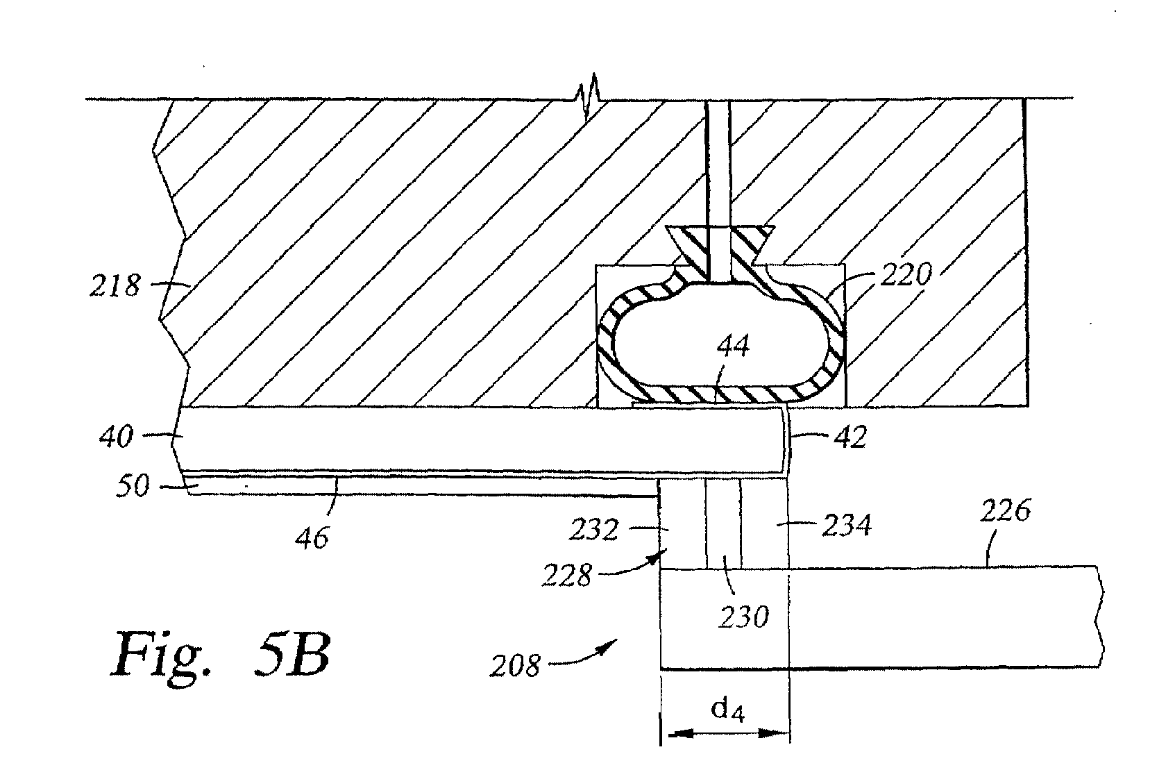
- Figure 5A is a cross sectional view of an electrochemical deposition cell adapted to achieve less than 3mm edge exclusion according to the invention.
- Figure 5B is a cross sectional detail view of an edge portion of the substrate disposed on a substrate holder and a cathode contact member according to the invention.
- Figure 6 is a cut-away perspective view of a cathode contact member according to the invention.
- Figure 7A is a cross sectional view of a de-plating cell having a de-plating substrate holder and a de-plating contact member according to the invention.
- Figure 7B is a cross sectional detail view of an edge portion of the substrate disposed on a de-plating substrate holder and a de-plating contact member according to the invention.
- Figure 8 is a cut-away perspective view of a de-plating contact member according to the invention.
- Figure 9A is a cross sectional view of a wet etch cell according to the invention.
- Figure 9B is a cross sectional detail view of an edge portion of the substrate disposed in a wet etch cell according to the invention.
- The present invention generally provides an apparatus and a method for forming a metal layer utilizing electrochemical deposition on a substrate having a dielectric layer formed thereon and a plurality of interconnect features, such as vias, contacts and lines, formed in the dielectric layer. The present invention achieves a number of commercial goals such as high throughput of the system and minimal edge exclusion on the substrate. Figure 3 is a flow diagram illustrating the method for forming a metal layer according to one aspect the invention. A substrate having, for example, a dielectric layer and an unfilled/etched interconnect feature structure (e.g., vias, contacts and dual damascene structures) formed in the dielectric layer is introduced into a physical vapor deposition chamber adapted to deposit a full coverage seed layer on the substrate. A full coverage seed layer is deposited on the substrate, including the peripheral portions of the substrate and the surfaces of the interconnect features thereon (Step 254). Prior to deposition of the seed layer, a full coverage barrier layer may be deposited on the substrate to protect against diffusion of subsequently deposited seed layer material into the dielectric layer on the substrate (Step 252). After the full coverage, seed layer has been formed, the substrate is then transferred into an electrochemical deposition cell adapted to provide electrochemical deposition of a metal layer having less than about 3mm edge exclusion, and a metal layer is electrochemically deposited on the substrate to fill the interconnect features, such as vias, contacts and lines (Step 256). The substrate is then transferred to a processing cell adapted to remove the remaining exposed seed layer on the peripheral portion of the substrate, including the bevel edge and the backside surface of the substrate (Step 258). The processing cell for removing the seed layer preferably comprises a de-plating cell, or alternatively, an etching cell. Alternatively, the electro-chemical deposition cell may be adapted to perform a de-plating process. After the seed layer has been removed from the peripheral portion of the substrate, the substrate is ready for other processing such as planarization and further processes to complete the formation of devices.
- Figure 4A is a cross sectional view of a high/medium density plasma physical vapor deposition chamber useful for forming full coverage layers according to the present invention. The PVD chamber as shown is known as an ionized metal plasma physical vapor deposition chamber or IMP-PVD chamber. Figure 4B is a cross sectional view of an edge portion of the substrate disposed in a PVD chamber configured for full coverage deposition as in Figure 4A. An example of a commercially available PVD chamber is the IMP® PVD chamber, available from Applied Materials, Inc., Santa Clara, California. Although the invention is described in reference to an IMP-PVD chamber, it is understood that the barrier layer and the seed layer can be deposited utilizing other PVD systems.
- Referring to Figures 4A and 4B, the IMP-
PVD deposition chamber 600 generally includes a chamber enclosure 602, asubstrate support member 604, atarget 606, a shield 608 and acoil 610. Thetarget 606 comprises a sputterable material and is disposed opposite thesubstrate support member 604. Thetarget 606 is electrically connected to aDC power supply 612, and can be biased by an RF power source (not shown) in addition to or instead of theDC power supply 612. The shield 608 generally surrounds the region between thetarget 606 and thesubstrate support member 604 and is typically grounded. The shield 608 includes an innerupturned wall 609 that supports ashield ring 624 when thesubstrate support member 604 is not moved to the substrate processing position. Thecoil 610 is disposed interior of the shield 608 and is connected to anRF power supply 614. A gas inlet 616 disposed through the enclosure 602 introduces one or more processing gases into the chamber during processing. Avacuum system 628 is connected to thechamber 600 through anexhaust port 630 to exhaust gases in the chamber and maintain a desired pressure in the chamber. Preferably, thevacuum system 628 comprises one or more vacuum pumps, turbo-molecular pumps, roughing pumps or cryopumps. Preferably, apower supply 632 is electrically connected to thesubstrate support member 604 to provide an electrical bias to the substrate during processing. Thepower supply 632 can be a DC power source, an RF power source, or a combination of DC and RF power sources. - The
substrate support member 604, preferably comprising an electrostatic chuck or a vacuum chuck, is attached to amovable shaft 618 disposed through the bottom of the enclosure 602. Themovable shaft 618 is connected to anactuator 620 which facilitates movement of thesubstrate support member 604 to various positions in the chamber, including a substrate processing position and a substrate transfer position. Aslit valve 626 disposed on a sidewall of the enclosure 602 facilitates transfer of substrates into and out of the chamber, which is typically performed utilizing a robot and robot blade (not shown). Asubstrate lift assembly 622 facilitates positioning of a substrate onto and off of thesubstrate support member 604 to cooperate with the robot blade during substrate transfer. During substrate transfer, thesubstrate support member 604 is lowered by theactuator 620 to a substrate transfer position at about the level of theslit valve 626. To transfer a substrate out of the chamber, thesubstrate lift assembly 622 lifts the substrate above thesubstrate support member 604, and a robot blade is extended through an openedslit valve 626 to a position below the substrate. Thesubstrate lift assembly 622 then lowers the substrate onto the robot blade, and the robot blade retracts out of the chamber with the substrate thereon. To transfer a substrate into the chamber, the robot blade extends into the chamber and positions a substrate above thesubstrate support member 604, and thesubstrate lift assembly 622 lifts the substrate off the robot blade so that the blade can be retracted. After the robot blade retracts out of the chamber, thesubstrate lift assembly 622 lowers the substrate onto thesubstrate support member 604. - As shown in Figures 4A and 4B, the
substrate support member 604 is raised to position the substrate thereon in a substrate processing position. At this position, a processing region is defined by the exposed surfaces of thetarget 606, the shield 608 and thesubstrate 40 on thesubstrate support member 604. Thesubstrate support member 604 includes adeposition ring 642 disposed on a peripheral edge of thesubstrate support member 604. During processing, theactuator 620 elevates thesubstrate support member 604 to a substrate processing position, where thedeposition ring 642 engages the bottom of theshield ring 624 and lifts theshield ring 624 off of the inner upturned wall of the shield 608. The inner portion of theshield ring 624 extends over an outer portion of thedeposition ring 642. Theshield ring 624 does not extend over theperipheral edge 42 of the substrate and allows full coverage deposition on thesubstrate 40. Thus, the substrate receives full deposition coverage over the whole substrate deposition surface and thesubstrate edge 42. In the configuration shown in Figures 4A and 4B, the substrate also receives partial deposition on the peripheral portion of thebackside surface 44 that extends outwardly from the substrate support. The full coverage deposition process provides aconformal seed layer 46 which extends over substantially all of the surface of the substrate on which the contacts in the cathode contact member of an electroplating system can be connected. By moving the contacts outwardly to the edge of the substrate, less than 3mm edge exclusion can be achieved as discussed below. - Typically, the substrate comprises a semiconductor wafer having a dielectric layer formed thereon, and a plurality of interconnect features, such as lines, vias, contacts, can be formed in the dielectric layer by etch processes. Deposition of dielectric layers and etching of interconnect features in the dielectric layers are generally known in the art and can be performed utilizing a variety of processes. Preferably, prior to deposition of the seed layer, a full coverage barrier layer is deposited over the substrate to protect against diffusion of subsequently deposited material into the dielectric layer on the substrate, or where the features contacts silicon, to prevent inter-diffusion of the silicon and conductor. For copper seed layers and copper metallization, the barrier layer material preferably comprises one or more materials selected from tantalum (Ta), tantalum nitride (TaNx), tungsten (W), tungsten nitride (WNx), titanium (Ti), titanium nitride (TiNx) and combinations thereof. Preferably, the barrier layer and the seed layer are deposited utilizing full coverage PVD chambers as described herein.
- Several parameters of the IMP-PVD process can be adjusted to achieve a desired barrier layer and seed layer deposition profile having acceptable sidewall and bottom coverage in high aspect ratio interconnect features. The IMP-PVD processing parameters, such as the processing pressure, the RF bias to the coil, the DC or RF bias to the target, and the DC or RF bias to the substrate, are adjusted to re-sputter deposition from the sidewall portions of the features to the base portions of the features. Particularly, the substrate bias during deposition is increased to effectuate an increased re-sputtering rate from deposited materials on the sidewall portions of the features and an increased deposition rate on the bottom of the feature. Typically, the IMP-PVD processing parameters are adjusted to achieve a ratio of sidewall re-sputtering rate to deposition rate of up to about 2:3. Preferably, the resulting deposition profile on the surfaces of the feature has a ratio of sidewall deposition thickness to base deposition thickness of between about 1:1 and 1:3. The chamber processing pressure is preferably maintained at between about 10 mTorr and about 100 mTorr, the RF source power to the IMP-PVD coil at between about 1000W and about 5000W, the target DC bias at between about 500W and about 3000W and substrate DC bias at between about 100W and about 500W.
- The seed layer preferably has a thickness between about 1500Å and about 2500Å over the field of the substrate, between about 150Å and about 300Å over the base surface of the feature and less than about 100Å, even more preferably, less than about 50Å, deposited on the sidewall portions of the feature. After the full coverage seed layer has been deposited over the substrate, the substrate is transferred into an electrochemical deposition ceil to form a metal layer and fill interconnect features.
- Figure 5A is a cross sectional view of an electrochemical deposition cell adapted to achieve less than 3mm edge exclusion according to the invention. Figure 5B is a cross sectional detail view of an edge portion of the substrate disposed on a substrate holder and a cathode contact member according to the invention. Although the invention is described utilizing one design of an electrochemical deposition cell, the inventors contemplate utilizing other electrochemical deposition cell designs adapted according to the invention to achieve an edge exclusion of less than about 3mm. Examples of electrochemical deposition cells include the Electra™ ECP System, available from Applied Material, Inc., Santa Clara, California, and the electrochemical deposition system described in commonly assigned and copending U.S. Patent Application No. 09/289,074, entitled "Electrochemical Deposition System," filed on April 8, 1999, which is hereby incorporated by reference in its entirety. After the full coverage seed layer has been deposited over the surfaces of the substrate, including the surfaces of the interconnect features, the substrate is transferred into the electrochemical deposition cell for electroplating a metal layer, such as copper, to fill or metallize the interconnect features.
- Referring to Figures 5A and 5B, the
electrochemical deposition cell 200 generally comprises anelectrolyte container 202, ananode 204, asubstrate holder 206, and acathode contact member 208. Theelectrolyte container 202 has a top opening adapted to receive a substrate disposed on the substrate holder and the cathode contact member. Theelectrolyte container 202 is connected to an electrolyte inlet 212 and anelectrolyte outlet 214. Theanode 204 is disposed in theelectrolyte container 202 and electrically connected to apower supply 216. Thesubstrate holder 206 preferably comprises avacuum chuck 218 and anannular bladder 220 surrounding thevacuum chuck 218. Thevacuum chuck 218 includes a plurality of vacuum holes or channels disposed across asubstrate support surface 224 of thesubstrate holder 206 through which a vacuum is provided to hold the substrate. Theannular bladder 220 is disposed around the substrate support surface and adapted to engage the peripheral portion of thebackside surface 44 of the substrate. Preferably, theannular bladder 220 comprises an inflatable bladder that provides a seal around the substrate backside edge and exerts pressure on the substrate to enhance contact between the substrate and the cathode contact member. Alternative embodiments of the bladder and the cathode contact member are described in commonly assigned and copending U.S. Patent Application No. 09/201,796 entitled "Inflatable Compliant Bladder Assembly", filed on November 30, 1998, and U.S. Patent Application No. 09/201,486 entitled "Cathode Contact Ring For Electrochemical Deposition", filed on November 30, 1998, which are hereby incorporated by reference in their entirety. - Figure 6 is a cut-away perspective view of a
cathode contact member 208 according to the invention. Referring to Figures 5A, 5B and 6, thecathode contact member 208 preferably comprises anannular body 226 having an inner diameter slightly smaller (i.e., less than about 3mm) than the diameter of the substrate to be processed. A compliantelectrical contact ring 228, preferably comprising a material that does not dissolve in the electrolyte, such as platinum, extends from an upper surface of the inner peripheral portion of theannular body 226. The compliantelectrical contact ring 228 comprises a plurality ofshort wires 230 disposed between an innercompliant sealing ring 232 and an outercompliant sealing ring 234. Theshort wires 230 are disposed at angle to the surface to be contacted to facilitate compliant contact with the substrate. As alternatives to the compliant electrical contact ring, the cathode contact member may include other electrical contact designs, such as individual curved or semi-spherical shaped contacts. - The
cathode contact member 208 is electrically connected to thepower supply 216, and the compliantelectrical contact ring 228 engages the peripheral portion of the substrate deposition surface to provide electrical contact between thecathode contact member 208 and theseed layer 46 on the substrate deposition surface. The compliantelectrical contact ring 228 also provides a seal with the substrate to prevent the electrolyte from reaching the peripheral portion of the substrate deposition surface, the substrate bevel edge and the substrate backside surface. Preferably, the compliantelectrical contact ring 228 physically contacts theseed layer 46 on the substrate deposition surface at less than about 3mm radially inward from theedge 42 of the substrate, as indicated by d4, and even more preferably, no more than about 2mm radially inward from theedge 42 of the substrate. The size of the edge exclusion is mainly dictated by the extent of the compliant electrical contact ring extending radially inward from the edge of the substrate. For example, a compliantelectrical contact ring 228 that physically contacts the substrate deposition surface at about 2mm radially inward from the edge of the substrate achieves about a 2mm edge exclusion from the electrochemical deposition. - During an electroplating process, the seed layer on the
substrate 40 is positioned in physical contact with thecathode contact member 208, and theannular bladder 220 is engaged to provide pressure against the backside of the substrate, which forces the surface of theseed layer 46 against the compliantelectrical contact ring 228 on thecathode contact member 208. Thepower supply 216 provides a negative voltage to thecathode contact member 208 and a forward plating current density across theseed layer 46 on the substrate plating surface to effectuate electrochemical deposition of the metal ions in the electrolyte onto the substrate plating surface. Thepower supply 216 also provides a positive voltage to theanode 204 to effectuate release of metal ions from thesoluble anode 204. The electrical power (i.e., voltage and current) supplied to the substrate plating surface is adjusted according to the electroplating solution used and desired deposition rate and characteristics. For example, to deposit a copper layer on a 200mm substrate using a soluble copper anode and an electroplating solution comprising copper sulfate, the cathode contact member is preferably biased to provide a forward plating current density across the substrate plating surface at between about 10 mA/cm2 and about 80 mA/cm2. The copper electroplating solution (i.e., electrolyte) comprises multi-components including copper electrolyte and additives such as suppressers and brighteners/accelerators. A detailed description of the electroplating chemistry, particularly the composition of the electrolyte and additives, is provided in commonly assigned and copending U.S. Patent Application No. 09/245,780, entitled "Electrodeposition Chemistry for Improved Filling of Apertures," filed on February 5, 1999, which is hereby incorporated by reference in its entirety. - After the
metal layer 50 has been formed on the substrate, the substrate is preferably transferred to a de-plating cell to remove the metal on the peripheral portion of the substrate, including the peripheral portion of the substrate deposition surface, the substrate bevel edge, and the peripheral portion of the substrate backside surface. Preferably, the de-plating cell utilizes an electrolyte or an etching solution that selectively dissolves the seed layer material (e.g., copper), but does not significantly dissolve or affect the barrier material or the substrate. - Figures 7A and 7B are cross sectional views illustrating a
de-plating cell 300 having ade-plating substrate holder 306 and ade-plating contact member 308 according to one aspect of the invention. Thede-plating cell 300 is separate from the plating cell to reduce contamination, and the de-plating process is performed utilizing a de-platingcathode contact member 308. Also, a separate de-plating cell facilitates removal of metal collected on the de-plating cathode contact member without introducing variations or compromising the quality of the contact surfaces of the cathode contact member that is used for the electroplating process. Alternatively, the electroplating cell, such as the cell shown in Figures 5A and 5B, can be adapted for use in de-plating processes as well, - The
de-plating cell 300 generally comprises anelectrolyte container 302, ananode 304 disposed in the electrolyte container, ade-plating substrate holder 306 and ade-plating contact member 308. Theelectrolyte container 302 has a top opening adapted to receive a substrate disposed on thede-plating substrate holder 306 and thede-plating contact member 308. Theelectrolyte container 302 is connected to anelectrolyte inlet 312 and anelectrolyte outlet 314. Theanode 304, preferably comprising a non-consumable anode, is disposed in theelectrolyte container 302 and electrically connected to apower supply 316. The electrolyte for the de-plating process comprises multi-components, including copper electrolyte and additives such as suppressers and brighteners/accelerators. The composition of the electrolyte used for the de-plating process may be the same as the electrolyte used for the plating process. - In one aspect, die
de-plating substrate holder 306 comprises avacuum chuck 318 and anannular seal 320 surrounding thevacuum chuck 318. Theannular seal 320 preferably comprises a compliant O-ring disposed in an annular groove on a substrate support surface of thede-plating substrate holder 306. Thevacuum chuck 318 includes a plurality of vacuum holes or channels disposed across thesubstrate support surface 324 of thesubstrate holder 306 through which a vacuum is provided to hold the substrate. Theannular seal 320 is disposed circumferentially on thesubstrate support surface 324 and adapted to engage an annular portion of the backside surface of the substrate. Thesubstrate holder 306 preferably has a smaller diameter than the diameter of the substrate to expose a peripheral portion of the substrate backside surface that has the seed layer deposited thereon, and theannular seal 320 engages the substrate at a position radially inward of die peripheral portion of the substrate backside surface to expose the seed layer to the de-plating solution. - Figure 8 is a cut-away perspective view of a
de-plating contact member 308. Referring to Figures 7A, 7B and 8, thede-plating contact member 308 preferably comprises anannular body 326 having a plurality of spokes orradial extensions 328 connected to a generally circularde-plating contact 330.Openings 329 between adjacentradial extensions 328 facilitate electrolyte flow to contact the peripheral portion of the substrate as well as exposed portions of the backside of the substrate. Thede-plating contact member 308 comprises a metal, such as platinum or stainless steel, that resists being dissolved by the electrolyte used in the de-plating process. Thede-plating contact 330 comprises an annular member disposed at a position that is radially inwardly from theedge 42 of thesubstrate 40 and adjacent theedge exclusion area 48 as shown in Figure 7B. Alternatively as shown in phantom in Figure 7B, the inner annularde-plating contact 330 is disposed at a position radially inward from theedge exclusion area 48 on the substrate. For example, for a substrate having ametal layer 50 electroplated with a 3mm edge exclusion area, thede-plating contact 330 is preferably disposed adjacent the substrate at a distance between about 0mm and about 6mm, as indicated by distance d5, from theedge 42 of thesubstrate 40. Thede-plating contact 330 may also comprise a plurality of individual contacts spaced substantially evenly around an annular region adjacent the edge exclusion area on the substrate, rather than the continuous annular ledge shown in Figure 8. - The following describes a process for de-plating the metal seed layer from the
edge exclusion area 48 and the seed layer on thebackside 44 and theedge 42 of the substrate. Thesubstrate 40 is introduced into a de-plating cell and positioned on thede-plating contact 330. Then, thede-plating substrate holder 306 is moved to a position to engage the backside of the substrate, and thevacuum chuck 318 is activated to securely hold the substrate on thesubstrate support surface 324. Thede-plating substrate holder 306 moves to position the substrate surface at a distance d3 which is less than 2mm away from the surface of thede-plating contact 330. The substrate surface can even be in physical contact with the surface of thede-plating contact 330 as long as there is sufficient contact resistance between the substrate surface and the surface of thede-plating contact 330. Typically, when no force is exerted to engage the substrate surface against thede-plating contact 330, sufficient contact resistance exist between the substrate surface and the surface of thede-plating contact 330 to facilitate a de-plating process as described herein. - To begin the de-plating process, the
de-plating substrate holder 306 with thesubstrate 40 thereon and thede-plating contact member 308 are positioned in theelectrolyte container 302 in contact with the electrolyte. The inventors have discovered that when a contact resistance exists between the substrate and the contact member, deposited metal on the substrate at locations adjacent the contact surface of the contact member is de-plated onto a contact member biased with a forward plating bias. When thede-plating contact 330 is biased with a forward plating bias, the power supply biases the de-plating contact member at a negative voltage and delivers a forward plating current as if a plating process were being performed. During this de-plating process, the metal on the peripheral region of the substrate adjacent the surface of thede-plating contact 330 serves as the anode which supplies the metal ions to be plated onto thede-plating contact 330. The de-plating rate varies across the substrate surface depending mainly on the distance and the effective resistance between thede-plating contact 330 and the substrate surface. For example, for an annular de-plating contact positioned adjacent an annular region inward from the edge of the substrate, the de-plating rate decreases dramatically from the annular region adjacent the surface of the de-plating contact toward the center of the substrate. Thus, the deposited metal on the central portions of the substrate remains substantially unaffected by the de-plating process. Typically, the power supply delivers a forward plating current density between about 10 mA/cm2 and about 80 mA/cm2 across the surface of thede-plating contact 330 for between about 1 second and about 20 seconds during the de-plating process. Higher current densities may provide faster de-plating rates and require less time to de-plate a metal layer. The de-plating process is stopped after the seed layer has been completely removed from the peripheral portions of the substrate. The substrate is removed from the electrolyte and a spin-dry process can be performed on the substrate to remove residual electrolyte from the substrate. The vacuum chuck is disengaged to release the substrate from thede-plating contact 330, and a robot transfers the substrate out of the de-plating cell. - Alternatively, the de-plating process is performed utilizing the same cell as the electroplating cell. The inventors have discovered that the metal on the substrate adjacent the cathode contact member is de-plated onto the cathode contact member when the bladder system is deflated to cause a contact resistance build up between the cathode contact surface and the metal layer. Preferably, the surface of cathode contacts are positioned at a distance less than about 2mm from the surface of the metal layer. When the bladder system is disengaged and does not exert pressure to the backside of the substrate, the metal layer on the substrate is de-plated onto the surfaces of the cathode contact member because of the contact resistance between the adjacent surfaces, even where the cathode contacts are disposed in physical contact with the surface of the metal layer.
- Another aspect of the invention provides a wet etch cell as an alternative to the de-plating cell for removing the metal seed layer on the peripheral portion of the substrate, including the peripheral portion of the substrate deposition surface, the substrate bevel edge, and the peripheral portion of the substrate backside surface.
- Figure 9A is a cross sectional view of a wet etch cell according to another embodiment of the invention. Figure 9B is a cross sectional view of an edge portion of the substrate disposed in a wet etch cell of Figure 9A. The
wet etch cell 400 generally comprises acontainer 402 and asubstrate support 404. Thecontainer 402 holds the etch solution and includes a top opening adapted to receive a substrate disposed on ansubstrate support 404. Thesubstrate holder 404 preferably comprises avacuum chuck 408 and aseal 410, such as an o-ring, disposed around thevacuum chuck 408. Alternatively, thesubstrate holder 404 comprises a gripper, such as a vacuum gripper. Thesubstrate support 404 is adapted to hold asubstrate 40 on the backside surface of the substrate and expose thesubstrate deposition surface 50, thesubstrate edge 42, and the peripheral portion of the substrate backside surface 44 to the etch solution in thecontainer 402. - During the wet etch process, the
substrate holder 404 submerges the substrate held thereon in the etching solution in theetching solution container 402. Typically, the etching solution comprises an etchant which dissolves the exposed metal into the solution. For example, the etching solution may comprise citric acid, citric acid diluted with hydrogen peroxide (H2O2) or other dilutants, or a combination of citric acid and sulfuric acid (H2SO4) to dissolve an exposed copper layer. Preferably, the etching solution is designed to provide selective etching of the seed layer material but leaves the barrier layer on the substrate. Alternatively, the etching solution is selected to dissolve various metal compositions, including metallic barrier layers, such as tantalum nitride (TaN) and titanium nitride (TiN). The etching solution may be heated by a heater thermally attached to the etching solution container to enhance the etching process, the etching results or the etching rate. Preferably, thesubstrate 40 is submerged in the etching solution for a calculated period of time to remove the metal seed layer on theperipheral portion 48 of the substrate deposition surface, thesubstrate edge 42, and the peripheral portion of thesubstrate backside surface 44. The calculated period of etch time, which varies with the etching solution being used, approximately equals to the thickness of the layer to be etched (Å) divided by the etch rate (Å/s). For example, when using an etching solution comprising citric acid at a temperature between about 10°C and about 70°C, a substrate having a copper seed layer between about 100Å and about 2500Å thick is submerged in the etching solution for between about 0.2 second and about 5 seconds to completely remove the copper seed layer from the peripheral portion of the substrate deposition surface, the substrate bevel edge, and the peripheral portion of the substrate backside surface. - Preferably, the electroplated
metal layer 50 is masked with an etch resist to prevent removal of the electroplated metal by the etching solution. Alternatively, the electroplated metal layer is unmasked during the wet etch process, and the electrochemical deposition is extended to provide a thicker electroplated metal layer which compensates for the thickness removed during the wet etch process. The thickness of the electrochemical deposited layer on the substrate can be increased to compensate for the amount of metal that will be de-plated or etched from the surface when the substrate is de-plated or etched to remove the seed layer on the peripheral portion of the substrate. Typically, since the seed layer is less than 10 percent of the total thickness of the electroplated metal layer, a 10% increase in the thickness of the electroplated metal layer or an increase corresponding to the thickness of the seed layer is sufficient to compensate for the de-plating effects. For example, for a 1000Å thick seed layer, the electro-chemical deposition process is extended to deposit an additional 1000Å over the desired thickness so that during the wet etch process the seed layer is completely removed and the desired thickness for the electroplated layer remains on the substrate. - The above described method for forming a metal layer on a substrate can be performed in commercially available integrated process platforms, such as the Electra™ ECP Cu System and the Endura® Electra™ Cu System, available from Applied Material, Inc., of Santa Clara, California. A substrate having a dielectric layer and interconnect features etched in the dielectric layer is introduced into a full coverage PVD chamber, and a full coverage barrier layer, comprising one or more materials selected from tantalum (Ta), tantalum nitride (TaNx), tungsten (W), tungsten nitride (WNx), titanium (Ti), titanium nitride (TiNx) and combinations thereof, is deposited over the substrate to protect against diffusion of subsequently deposited seed layer material into the dielectric layer on the substrate. The full coverage barrier layer is deposited to a thickness between about 50Å and 250Å over the surfaces inside the interconnect features utilizing an IMP-PVD chamber having the barrier material (e.g., tantalum, titanium or tungsten) and the processing parameters listed in Table 1. To facilitate reactive sputtering for forming films incorporating nitrogen, nitrogen gas may be flowed into the chamber at between about 500 sccm and about 2000 sccm during the sputtering process.
Chamber Processing Parameters For Deposition Of Barrier Layer and Seed Layer Chamber Parameter Setting Chamber Pressure 20 mT to 100 mT RF Power to Coil 1000W to 5000W Target Bias Power 500 W to 3000W Substrate DC Bias Power 100W to 500W Argon Flow 50 sccm to 500 sccm Processing Time 30 seconds to 90 seconds - A seed layer is deposited over the barrier layer utilizing an IMP-PVD chamber having a copper target. The seed layer is deposited to a thickness of between about 1500Å and about 2500Å over substantially the field of the substrate and a thickness of between about 50Å and about 250Å over the barrier layer surfaces inside the interconnect features utilizing the parameters listed in Table I utilizing an IMP-PVD chamber having a target having the seed layer material (e.g., copper).
- The substrate is then transferred into an electroplating cell, and a metal layer, typically between about 1µm and about 2 µm thick, is electrochemically deposited over the seed layer on the substrate to fill the interconnect features, such as vias, contacts and lines. The electrochemical deposition utilizing the above-described cathode contact member forms a metal layer over the substrate except for an annular portion of the substrate (i.e., less than about 3mm edge exclusion) masked by the cathode contact member. The electrochemical deposition process is preferably performed using a soluble copper anode and an electroplating solution comprising copper sulfate, and the cathode contact member is preferably biased to provide a forward plating current density across the substrate plating surface of between about 10mA/cm2 and about 80mA/cm2.
- After the electroplating process, the substrate is then transferred to a de-plating cell to remove the exposed seed layer on the peripheral portion of the substrate. The de-plating substrate holder immerses the substrate in the electrolyte, and the de-plating contact member is positioned adjacent a peripheral portion of the substrate. The de-plating process time is adjusted according to the thickness of the seed layer and the de-plating rate. Preferably, the power supply delivers a forward plating current density between about 10 mA/cm2 and about 80 mA/cm2 across the surface of the de-plating contact member for between about 1 second and about 20 seconds during the de-plating process to remove (i.e., de-plate) a seed layer up to about 2500Å thick on the peripheral portion of the substrate. After the seed layer has been removed from the peripheral portion of the substrate, the substrate is typically planarized to prepare the surface for further processing and completion of the devices.
- While foregoing is directed to the preferred embodiment of the present invention, other and further embodiments of the invention may be devised without departing from the basic scope thereof, and the scope thereof is determined by the claims that follow.
Claims (20)
- A method for forming a metal layer on a substrate, comprising:a) depositing a full coverage seed layer over the substrate;b) electrochemically depositing a metal layer over the seed layer; andc) removing exposed seed layer from an annular edge portion of the substrate.
- A method as claimed in claim 1 wherein the full coverage seed layer is deposited utilizing a full coverage physical vapor deposition chamber.
- A method as claimed in claim 1 or claim 2, wherein the step of removing the exposed seed layer comprises:i) positioning the substrate in a de-plating cell;ii) positioning a de-plating cathode contact member adjacent the substrate; andiii) applying a forward plating bias to the cathode contact member.
- A method as claimed in claim, 3, wherein the de-plating cathode contact member comprises an annular contact surface positioned adjacent an annular peripheral portion of the substrate.
- A method as claimed in claim 4, wherein the de-plating cathode contact member is positioned at less than about 6mm radially inward from an edge of the substrate.
- A method as claimed in claim 4, wherein the de-plating cathode contact member is positioned at less than about 2mm from a surface of the substrate.
- A method as claimed in any of claims 1 to 6, wherein the step of electrochemically depositing a metal layer over the seed layer comprises:i) electrically contacting a cathode contact member with the seed layer at a peripheral portion fo the substrate that is less than about 3mm from an edge of the substrate; andii) positioning the substrate in an electroplating solution in an electroplating cell.
- A method as claimed in claim 7, wherein the step of electrochemically depositing a metal layer over the seed layer further comprises:iii) securing the substrate on a substrate holder having an inflatable bladder disposed at a peripheral portion of a back surface of the substrate; andiv) inflating the bladder against the peripheral portion of the back surface of the substrate.
- A method as claimed in claim 8, wherein the step of removing the exposed seed layer comprises:i) deflating the inflatable bladder; andii) positioning the cathode contact member between about 0mm and about 2mm from the substrate; andiii) applying a forward plating bias to the cathode contact member.
- A method as claimed in claim 1 or claim 2, wherein the step of removing the exposed seed layer comprises:i) positioning the substrate in a wet etch cell; andii) contacting the exposed seed layer with an etching solution.
- A method for forming a metal layer on a substrate, comprising:a) depositing a full coverage seed layer over the substrate utilizing a full coverage physical vapor deposition chamber;b) electrochemically depositing a metal layer over the seed layer, comprising:i) electrically contacting a cathode contact member with the seed layer at a peripheral portion of the substrate that is less than about 3mm from an edge of the substrate; andii) positioning the substrate in an electroplating solution in an electroplating cell; andc) removing exposed seed layer from an annular edge portion of the substrate, comprising:i) positioning the substrate in a de-plating cell;ii) positioning a de-plating cathode contact member adjacent the substrate; andiii) applying a forward plating bias to the cathode contact member.
- A method as claimed in claim 11, wherein the de-plating cathode contact member comprises an annular contact surface positioned adjacent an annular peripheral portion of the substrate.
- A method as claimed in claim 12, wherein the de-plating cathode contact member is positioned at less than about 6mm radially inward from an edge of the substrate.
- A method as claimed in claim 13, wherein the de-plating cathode contact member is positioned at less than about 2mm from the exposed seed layer on the substrate.
- An apparatus for forming a metal layer on a substrate, comprising:a) an electrochemical deposition cell having a cathode contact member adapted to contact a peripheral portion of a substrate at less than about 3mm from an edge of the substrate;b) a processing cell adapted to remove exposed seed layer on a peripheral portion of the substrate; andc) a transfer chamber having a robot adapted to transfer a substrate between the electrochemical deposition cell and the processing cell for removing exposed seed layer.
- An apparatus as claimed in claim 15, wherein the elctrochemical deposition cell comprises:i) a substrate holder having vacuum chuck and a seal disposed around the vacuum chuck;ii) a cathode contact member adapted to contact an annular peripheral portion of the substrate;iii) an electrolyte container having an opening adapted to receive the substrate; andiv) an anode disposed in the electrolyte container.
- An apparatus as claimed in claim 16, wherein the cathode contact member includes an annular compliant member adapted to sealingly engage the annular peripheral portion fo the substrate.
- An apparatus as claimed in any of claims 1 to 13, wherein the processing cell comprises:i) a substrate support member adapted to hold the substrate and expose a peripheral portion of the substrate; andii) a solution container having an opening adapted to receive the substrate.
- An apparatus as claimed in claim 18, wherein the processing cell further comprises:iii) an anode disposed in the chemical solution container; andiv) a de-plating contact member disposed adjacent a peripheral portion of the substrate.
- An apparatus as claimed in claim 15, wherein the processing cell comprises a wet etch cell.
Applications Claiming Priority (2)
| Application Number | Priority Date | Filing Date | Title |
|---|---|---|---|
| US09/443,832 US6423636B1 (en) | 1999-11-19 | 1999-11-19 | Process sequence for improved seed layer productivity and achieving 3mm edge exclusion for a copper metalization process on semiconductor wafer |
| US443832 | 1999-11-19 |
Publications (2)
| Publication Number | Publication Date |
|---|---|
| EP1101839A2 true EP1101839A2 (en) | 2001-05-23 |
| EP1101839A3 EP1101839A3 (en) | 2004-01-21 |
Family
ID=23762366
Family Applications (1)
| Application Number | Title | Priority Date | Filing Date |
|---|---|---|---|
| EP00310208A Withdrawn EP1101839A3 (en) | 1999-11-19 | 2000-11-17 | Methods and apparatus for forming metal layers on substrates |
Country Status (5)
| Country | Link |
|---|---|
| US (1) | US6423636B1 (en) |
| EP (1) | EP1101839A3 (en) |
| JP (1) | JP5367930B2 (en) |
| KR (1) | KR20010051801A (en) |
| TW (1) | TW508661B (en) |
Cited By (1)
| Publication number | Priority date | Publication date | Assignee | Title |
|---|---|---|---|---|
| US6689418B2 (en) | 2001-08-03 | 2004-02-10 | Applied Materials Inc. | Apparatus for wafer rinse and clean and edge etching |
Families Citing this family (26)
| Publication number | Priority date | Publication date | Assignee | Title |
|---|---|---|---|---|
| US6413436B1 (en) * | 1999-01-27 | 2002-07-02 | Semitool, Inc. | Selective treatment of the surface of a microelectronic workpiece |
| US6913680B1 (en) | 2000-05-02 | 2005-07-05 | Applied Materials, Inc. | Method of application of electrical biasing to enhance metal deposition |
| WO2001090446A2 (en) * | 2000-05-23 | 2001-11-29 | Applied Materials, Inc. | Method and apparatus to overcome anomalies in copper seed layers and to tune for feature size and aspect ratio |
| JP4055334B2 (en) * | 2000-06-13 | 2008-03-05 | ソニー株式会社 | Manufacturing method of semiconductor device |
| US6534394B1 (en) * | 2000-09-13 | 2003-03-18 | International Business Machines Corporation | Process to create robust contacts and interconnects |
| CN100469948C (en) * | 2000-10-03 | 2009-03-18 | 应用材料有限公司 | Method and associated apparatus for tilting a substrate upon entry for metal deposition |
| US7189647B2 (en) | 2001-04-05 | 2007-03-13 | Novellus Systems, Inc. | Sequential station tool for wet processing of semiconductor wafers |
| US6572755B2 (en) * | 2001-04-11 | 2003-06-03 | Speedfam-Ipec Corporation | Method and apparatus for electrochemically depositing a material onto a workpiece surface |
| US6908540B2 (en) * | 2001-07-13 | 2005-06-21 | Applied Materials, Inc. | Method and apparatus for encapsulation of an edge of a substrate during an electro-chemical deposition process |
| KR100440261B1 (en) * | 2001-12-22 | 2004-07-15 | 주식회사 하이닉스반도체 | Method of manufacturing a metal line in semiconductor device |
| US6733829B2 (en) * | 2002-03-19 | 2004-05-11 | Lsi Logic Corporation | Anti-binding deposition ring |
| US6911136B2 (en) * | 2002-04-29 | 2005-06-28 | Applied Materials, Inc. | Method for regulating the electrical power applied to a substrate during an immersion process |
| US7067045B2 (en) * | 2002-10-18 | 2006-06-27 | Applied Materials, Inc. | Method and apparatus for sealing electrical contacts during an electrochemical deposition process |
| US7025862B2 (en) * | 2002-10-22 | 2006-04-11 | Applied Materials | Plating uniformity control by contact ring shaping |
| KR20040072446A (en) * | 2003-02-12 | 2004-08-18 | 삼성전자주식회사 | Method of selectively removing metal on a semiconductor wafer edge |
| US20040229002A1 (en) * | 2003-05-15 | 2004-11-18 | 3D Systems, Inc. | Stereolithographic seal and support structure for semiconductor wafer |
| US7285195B2 (en) * | 2004-06-24 | 2007-10-23 | Applied Materials, Inc. | Electric field reducing thrust plate |
| US20090304914A1 (en) * | 2006-08-30 | 2009-12-10 | Lam Research Corporation | Self assembled monolayer for improving adhesion between copper and barrier layer |
| US20060175201A1 (en) * | 2005-02-07 | 2006-08-10 | Hooman Hafezi | Immersion process for electroplating applications |
| US7520969B2 (en) * | 2006-03-07 | 2009-04-21 | Applied Materials, Inc. | Notched deposition ring |
| US8062487B2 (en) * | 2007-06-25 | 2011-11-22 | United Microelectronics Corp. | Wafer supporting device of a sputtering apparatus |
| WO2011103214A1 (en) * | 2010-02-16 | 2011-08-25 | Cypress Semiconductor Corporation | Integrated shielding for wafer plating |
| US9905443B2 (en) * | 2011-03-11 | 2018-02-27 | Applied Materials, Inc. | Reflective deposition rings and substrate processing chambers incorporating same |
| CN108291325B (en) * | 2015-12-04 | 2019-12-20 | 盛美半导体设备(上海)有限公司 | Substrate holding device |
| KR102323877B1 (en) * | 2016-09-28 | 2021-11-10 | 한국전자통신연구원 | Apparatus for electroplating |
| CN114959854B (en) | 2021-02-24 | 2024-02-13 | 株式会社东芝 | Jig for manufacturing semiconductor device and method for manufacturing semiconductor device |
Citations (2)
| Publication number | Priority date | Publication date | Assignee | Title |
|---|---|---|---|---|
| WO1999046064A1 (en) * | 1998-03-13 | 1999-09-16 | Semitool, Inc. | Selective treatment of the surface of a microelectronic workpiece |
| US6056869A (en) * | 1998-06-04 | 2000-05-02 | International Business Machines Corporation | Wafer edge deplater for chemical mechanical polishing of substrates |
Family Cites Families (26)
| Publication number | Priority date | Publication date | Assignee | Title |
|---|---|---|---|---|
| US3835017A (en) * | 1972-12-22 | 1974-09-10 | Buckbee Mears Co | Reusable shields for selective electrodeposition |
| EP0076569B1 (en) | 1981-10-01 | 1986-08-27 | EMI Limited | Electroplating arrangements |
| JPS58182823A (en) | 1982-04-21 | 1983-10-25 | Nec Corp | Plating apparatus for semiconductor wafer |
| US4428815A (en) | 1983-04-28 | 1984-01-31 | Western Electric Co., Inc. | Vacuum-type article holder and methods of supportively retaining articles |
| US4605483A (en) * | 1984-11-06 | 1986-08-12 | Michaelson Henry W | Electrode for electro-plating non-continuously conductive surfaces |
| JPS63118093A (en) | 1986-11-05 | 1988-05-23 | Tanaka Electron Ind Co Ltd | Method for tinning electronic parts |
| US5230743A (en) * | 1988-05-25 | 1993-07-27 | Semitool, Inc. | Method for single wafer processing in which a semiconductor wafer is contacted with a fluid |
| US5224504A (en) * | 1988-05-25 | 1993-07-06 | Semitool, Inc. | Single wafer processor |
| US5235995A (en) * | 1989-03-27 | 1993-08-17 | Semitool, Inc. | Semiconductor processor apparatus with dynamic wafer vapor treatment and particulate volatilization |
| US5316974A (en) * | 1988-12-19 | 1994-05-31 | Texas Instruments Incorporated | Integrated circuit copper metallization process using a lift-off seed layer and a thick-plated conductor layer |
| US5222310A (en) * | 1990-05-18 | 1993-06-29 | Semitool, Inc. | Single wafer processor with a frame |
| US5259407A (en) * | 1990-06-15 | 1993-11-09 | Matrix Inc. | Surface treatment method and apparatus for a semiconductor wafer |
| US5256274A (en) * | 1990-08-01 | 1993-10-26 | Jaime Poris | Selective metal electrodeposition process |
| JPH04131395A (en) | 1990-09-21 | 1992-05-06 | Toshiba Corp | Method and device for plating semiconductor wafer |
| JP2697773B2 (en) | 1991-03-11 | 1998-01-14 | 日本エレクトロプレイテイング・エンジニヤース 株式会社 | Plating method |
| JP3200468B2 (en) * | 1992-05-21 | 2001-08-20 | 日本エレクトロプレイテイング・エンジニヤース株式会社 | Wafer plating equipment |
| JPH0617291A (en) | 1992-07-03 | 1994-01-25 | Nec Corp | Metal plating device |
| US5486282A (en) * | 1994-11-30 | 1996-01-23 | Ibm Corporation | Electroetching process for seed layer removal in electrochemical fabrication of wafers |
| US5807469A (en) | 1995-09-27 | 1998-09-15 | Intel Corporation | Flexible continuous cathode contact circuit for electrolytic plating of C4, tab microbumps, and ultra large scale interconnects |
| KR20000057470A (en) * | 1996-12-16 | 2000-09-15 | 포만 제프리 엘 | Electroplated interconnection structures on integrated circuit chips |
| EP1027481A1 (en) * | 1997-09-30 | 2000-08-16 | Semitool, Inc. | Electroplating system having auxiliary electrode exterior to main reactor chamber for contact cleaning operations |
| US6156167A (en) * | 1997-11-13 | 2000-12-05 | Novellus Systems, Inc. | Clamshell apparatus for electrochemically treating semiconductor wafers |
| US5897379A (en) * | 1997-12-19 | 1999-04-27 | Sharp Microelectronics Technology, Inc. | Low temperature system and method for CVD copper removal |
| US6140234A (en) * | 1998-01-20 | 2000-10-31 | International Business Machines Corporation | Method to selectively fill recesses with conductive metal |
| US6416647B1 (en) * | 1998-04-21 | 2002-07-09 | Applied Materials, Inc. | Electro-chemical deposition cell for face-up processing of single semiconductor substrates |
| US6113771A (en) * | 1998-04-21 | 2000-09-05 | Applied Materials, Inc. | Electro deposition chemistry |
-
1999
- 1999-11-19 US US09/443,832 patent/US6423636B1/en not_active Expired - Fee Related
-
2000
- 2000-11-16 TW TW089124306A patent/TW508661B/en not_active IP Right Cessation
- 2000-11-17 EP EP00310208A patent/EP1101839A3/en not_active Withdrawn
- 2000-11-18 KR KR1020000068721A patent/KR20010051801A/en not_active Application Discontinuation
- 2000-11-20 JP JP2000393798A patent/JP5367930B2/en not_active Expired - Fee Related
Patent Citations (2)
| Publication number | Priority date | Publication date | Assignee | Title |
|---|---|---|---|---|
| WO1999046064A1 (en) * | 1998-03-13 | 1999-09-16 | Semitool, Inc. | Selective treatment of the surface of a microelectronic workpiece |
| US6056869A (en) * | 1998-06-04 | 2000-05-02 | International Business Machines Corporation | Wafer edge deplater for chemical mechanical polishing of substrates |
Cited By (1)
| Publication number | Priority date | Publication date | Assignee | Title |
|---|---|---|---|---|
| US6689418B2 (en) | 2001-08-03 | 2004-02-10 | Applied Materials Inc. | Apparatus for wafer rinse and clean and edge etching |
Also Published As
| Publication number | Publication date |
|---|---|
| KR20010051801A (en) | 2001-06-25 |
| US6423636B1 (en) | 2002-07-23 |
| TW508661B (en) | 2002-11-01 |
| EP1101839A3 (en) | 2004-01-21 |
| JP5367930B2 (en) | 2013-12-11 |
| JP2001240997A (en) | 2001-09-04 |
Similar Documents
| Publication | Publication Date | Title |
|---|---|---|
| US6423636B1 (en) | Process sequence for improved seed layer productivity and achieving 3mm edge exclusion for a copper metalization process on semiconductor wafer | |
| US6399479B1 (en) | Processes to improve electroplating fill | |
| US6328871B1 (en) | Barrier layer for electroplating processes | |
| US6786996B2 (en) | Apparatus and method for edge bead removal | |
| US7138014B2 (en) | Electroless deposition apparatus | |
| US6503375B1 (en) | Electroplating apparatus using a perforated phosphorus doped consumable anode | |
| US7837841B2 (en) | Apparatuses for electrochemical deposition, conductive layer, and fabrication methods thereof | |
| US6162726A (en) | Gas shielding during plating | |
| US8513124B1 (en) | Copper electroplating process for uniform across wafer deposition and void free filling on semi-noble metal coated wafers | |
| US6280581B1 (en) | Method and apparatus for electroplating films on semiconductor wafers | |
| US20030140988A1 (en) | Electroless deposition method over sub-micron apertures | |
| US8703615B1 (en) | Copper electroplating process for uniform across wafer deposition and void free filling on ruthenium coated wafers | |
| US7416975B2 (en) | Method of forming contact layers on substrates | |
| WO2002019418A2 (en) | Method for achieving copper fill of high aspect ratio interconnect features | |
| US20030143837A1 (en) | Method of depositing a catalytic layer | |
| US6808612B2 (en) | Method and apparatus to overcome anomalies in copper seed layers and to tune for feature size and aspect ratio | |
| US6708701B2 (en) | Capillary ring | |
| US20030073320A1 (en) | Method for preventing surface corrosion in an edge bead removal process | |
| US20040004004A1 (en) | Method for reducing cu surface defects following cu ECP | |
| US6652726B1 (en) | Method for reducing wafer edge defects in an electrodeposition process | |
| US7226860B2 (en) | Method and apparatus for fabricating metal layer | |
| US6797144B2 (en) | Method for reducing surface defects in an electrodeposition process | |
| US20100032315A1 (en) | Electrolytic processing apparatus and electrolytic processing method |
Legal Events
| Date | Code | Title | Description |
|---|---|---|---|
| PUAI | Public reference made under article 153(3) epc to a published international application that has entered the european phase |
Free format text: ORIGINAL CODE: 0009012 |
|
| AK | Designated contracting states |
Kind code of ref document: A2 Designated state(s): AT BE CH CY DE DK ES FI FR GB GR IE IT LI LU MC NL PT SE TR |
|
| AX | Request for extension of the european patent |
Free format text: AL;LT;LV;MK;RO;SI |
|
| PUAL | Search report despatched |
Free format text: ORIGINAL CODE: 0009013 |
|
| AK | Designated contracting states |
Kind code of ref document: A3 Designated state(s): AT BE CH CY DE DK ES FI FR GB GR IE IT LI LU MC NL PT SE TR |
|
| AX | Request for extension of the european patent |
Extension state: AL LT LV MK RO SI |
|
| RIC1 | Information provided on ipc code assigned before grant |
Ipc: 7C 23F 1/02 B Ipc: 7C 25F 3/14 B Ipc: 7C 25D 7/12 A |
|
| AKX | Designation fees paid | ||
| REG | Reference to a national code |
Ref country code: DE Ref legal event code: 8566 |
|
| STAA | Information on the status of an ep patent application or granted ep patent |
Free format text: STATUS: THE APPLICATION IS DEEMED TO BE WITHDRAWN |
|
| 18D | Application deemed to be withdrawn |
Effective date: 20040608 |