EP1101187B1 - Anordnung zur erfassung von oberflächenstrukturen von fingern und/oder handinnenflächen - Google Patents
Anordnung zur erfassung von oberflächenstrukturen von fingern und/oder handinnenflächen Download PDFInfo
- Publication number
- EP1101187B1 EP1101187B1 EP00942006A EP00942006A EP1101187B1 EP 1101187 B1 EP1101187 B1 EP 1101187B1 EP 00942006 A EP00942006 A EP 00942006A EP 00942006 A EP00942006 A EP 00942006A EP 1101187 B1 EP1101187 B1 EP 1101187B1
- Authority
- EP
- European Patent Office
- Prior art keywords
- structures
- reference structures
- assembly
- beam path
- image
- Prior art date
- Legal status (The legal status is an assumption and is not a legal conclusion. Google has not performed a legal analysis and makes no representation as to the accuracy of the status listed.)
- Expired - Lifetime
Links
Images



Classifications
-
- G—PHYSICS
- G06—COMPUTING OR CALCULATING; COUNTING
- G06V—IMAGE OR VIDEO RECOGNITION OR UNDERSTANDING
- G06V40/00—Recognition of biometric, human-related or animal-related patterns in image or video data
- G06V40/10—Human or animal bodies, e.g. vehicle occupants or pedestrians; Body parts, e.g. hands
- G06V40/12—Fingerprints or palmprints
- G06V40/13—Sensors therefor
-
- G—PHYSICS
- G06—COMPUTING OR CALCULATING; COUNTING
- G06V—IMAGE OR VIDEO RECOGNITION OR UNDERSTANDING
- G06V10/00—Arrangements for image or video recognition or understanding
- G06V10/10—Image acquisition
- G06V10/12—Details of acquisition arrangements; Constructional details thereof
- G06V10/14—Optical characteristics of the device performing the acquisition or on the illumination arrangements
- G06V10/145—Illumination specially adapted for pattern recognition, e.g. using gratings
Definitions
- the invention relates to an arrangement for detecting the surface structures of fingers, palms of the hand resting on an image scanning surface or others Skin areas, wherein the image scanning surface is formed on a scanning prism, in An illumination beam path is directed onto the image scanning surface inside the scanning prism and the light reflected from there onto the receiving surface of an optoelectronic Detection device meets.
- Arrangements of this type are in which Image information can be captured by scanning, device control and to calibrate to ensure functionality and accuracy requirements.
- Reference structures are attached, which are repeated over the course of the operating period serve as a basis for comparison with the results obtained with the same arrangement be achieved.
- users or service companies can check from time to time whether the quality parameters have been maintained are or due to any influences, such as aging or Wear of assemblies, deviations that have to be corrected. Checks of the device function are often also after a device disassembly, for cleaning purposes, required.
- the reference structures are applied to a carrier in the form of test structures, For example, on a slide to check the device function on the image sensing surface is launched.
- the test structures are recorded with the device and then compared the result of the recording with the test structure. Based this comparison, a statement is possible as to whether the arrangement meets the quality requirements still corresponds or changes have occurred. After that is remove the film with the test structures from the image sensing area, which is now again to record the surface structures of fingers or palms stands.
- the invention is based on the object the sources of errors and the possibilities of errors when checking arrangements for detecting the surface structures of those lying on an image scanning surface To reduce fingers or palms.
- arrangements of the type described in the introduction provide that part of the illuminating beam path or a separate illuminating beam path on reference structures and from there to the receiving surface of the optoelectronic Detection device is directed, the detection of the surface structures and the detection of the reference structures separate sub-areas of the Are reserved.
- the reference structures are applied to the image scanning surface in a fixed position, the Reference structures on the one hand and the support of the fingers or the palms of the hands on the other hand, separate, non-overlapping partial areas of the image scanning area are reserved and a common lighting beam path for this Sub-areas is provided. This will not help to perform the device test the areas of the image scanning area that are required for placing the finger or Palms are provided.
- a major advantage is that the detection of finger or Handprints and taking pictures of the reference structures no longer exclude each other, consequently no longer just in time, but can also be run simultaneously. It is also a falsification of the Test results due to contamination, which is caused by the application of the fingers or Hands have, at least for the areas of the image scanning area that correspond to the reference structures are reserved, as well as the occurrence of errors that occur from the introduction of optical intermediate layers (oil, water) between the image scanning surface and a portable carrier provided with the reference structures can result. The disadvantages of the prior art are thus eliminated.
- the reference structures are immediate applied to the image sensing surface, i.e. they are arranged in the object plane.
- the reference structures are also immobile, but outside the object level, for example at the entrance surface for the illumination beam path and / or at the exit surface for the radiation reflected by the image scanning surface are positioned. In this way, the reference structures are achieved with the greatest reliability removed from contact with the finger to be imaged or the palm of the hand are.
- the optoelectronic detection device with an evaluation circuit linked in which the images obtained from the reference structures reflect the actual state characterize the arrangement, a comparison with electronically stored, subjected to the data specifying the target state and from this comparison Conclusions on compliance or non-compliance with device-specific Quality parameters are drawn. This is an automatic check possible.
- a control circuit is exemplary for each commissioning and / or after each expiration a recording of the reference structures and the predetermined operating time Comparison of the recorded images with the stored data is caused. If this comparison leads to a negative result, triggering a Warning signals, an error message on the device display or by issuing a Switch-off impulse to the device control the incorrect detection of finger or Handprints can be prevented if minimum requirements are not met are.
- a cover can be placed over the reference structures applied to the image scanning area be provided. This prevents the reference structures of the are constantly exposed to fingers or hands while doing so pollute.
- the light entry surface or the light exit surface on the scanning prism it is conceivable to have an optical device for mirroring and / or to provide reference structures in the illumination beam path, so that image information from reference structures is also available in this way get the receiving surface of the optoelectronic detection device and in the above-described way of calibrating the arrangement can.
- Line marks of different line widths are, for example, reference structures as well as different line spacings and orientations. So that is special the contrast transfer function (CTF) can be determined, as the basis for the evaluation of the modulation transfer (modulation transfer Function - MTF) is used. It is also conceivable to use structures with high-contrast light-dark and to provide dark-light transitions in the horizontal and vertical directions, so that the MTF can be checked by Fourier analysis.
- CTF contrast transfer function
- MTF modulation transfer Function
- An empty field can also be provided under the reference structures Checking the linearity and the noise of the arrangement is used by at constant Illumination of the shutter of the detection device in defined steps adjusted and the respective output signal obtained with those retrievable from the memory Data is compared.
- test marks arranged at a defined distance from one another to be provided, which are used to check the image scale. That's how it is Review of the imaging scale also possible at intervals, by comparing the respective measurement results with those saved during production Values based on the two directions of expansion of the image scanning surface be placed.
- the object of the invention continues also solved in that in the illumination beam path, on the object surface and / or in the radiation reflected by the image scanning surface semi-transparent reference structures are introduced, both the surface structure to be recorded (the finger or palm) as well as the semi-transparent reference structures are exposed to the radiation and onto the receiving surface of the detection device striking radiation both the image information about the surface structure as well as the image information about the reference structures.
- the reference structures can be positioned so that they are different from the one to be detected Surface structure are covered, i.e. neither from the beam path nor Separate areas of the reception area are used only for recording the Surface structure on the one hand and only the acquisition of the reference structures otherwise reserved.
- the target gray values are advantageously determined for each individual sensor with a uniformly bright, structure-free image, and a second arithmetic function is also provided, by means of which the determined actual gray value of each image element ij is multiplied by the associated correction factor k ij .
- the correct correction values k ij result in a structure-free, uniformly bright image. If this does not occur, the correction values k ij must be read in again.
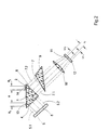
- Fig.1 an arrangement for taking fingerprints is shown, as they is known from the prior art.
- a finger 3 On the image scanning surface 1 of a scanning prism 2 a finger 3 is placed here, from which the impression is to be recorded.
- the scanning prism 2 has an entrance surface 4 for an illumination beam path 5 and a Exit surface 6 for that reflected within the scanning prism 2 from the image scanning surface 1 Light, hereinafter referred to as object beam path 7.
- the illuminating beam path 5 starts from an illuminating source 8, which for example as a two-dimensional arrangement of a variety of light-emitting Diodes (LEDs) with a downstream diffuser is formed.
- the lighting beam path 5 is inside the scanning prism 2 at an angle ⁇ on the image scanning surface 1 aimed at obtaining images of the fingerprint the principle of disturbed total reflection.
- the object beam path 7 is through a correction prism 9 and an objective 10 on the photosensitive receiving surface 11 of an optoelectronic detection device 12 directed.
- the receiving surface 11 is exemplary of a large number formed by individual sensors arranged in an orthogonal grid, and the Optoelectronic detection device 12 is part of a CCD camera that is in itself usually with an evaluation circuit for those that can be tapped at their output electronic image information is linked.
- Fig. 1 it can also be seen that only one area of the image scanning area 1 with the width a for laying on the finger (or several fingers or one palm) is provided while the edge areas are unused. Also from the Reception area 11 is used only an area in the plane of the 1 has the width c and on which the object beam path 7 is focused.
- Reference structures 13 are applied in the edge regions of the image scanning area 1 designated a 1 and a 2 , which lie outside the width a provided for the acquisition of the finger or handprint images .
- Radiation components 5.1 and 5.2 of the illumination beam path 5 hit these reference structures 13, and the radiation components 5.1 and 5.2 of the illuminating radiation reflected by the edge regions a 1 and a 2 reach the receiving surface 11 as radiation components 7.1 and 7.2 of the object beam path 7, where they coincide with c 1 and c 2 meet designated edge areas.
- the edge areas c 1 and c 2 are outside the width c, which is reserved for capturing the finger or handprint images.
- the reference structures 13 are designed such that their received by the optoelectronic detection device 12 and sent to the Evaluation circuit passed images a comparison with electronically stored Data that serve as a measure of the quality parameters of the arrangement can and as a result of this comparison on compliance or on Deviations can be closed.
- a top view of the image scanning area 1 it can be seen that the area section determined by a and b is provided for taking finger or handprint images, while the edge areas a 1 , a 2 , b 1 and b 2 respectively Application of reference structures are reserved.
- the edge areas a 1 and a 2 of the image sensing area 1 correspond to the edge areas c 1 and c 2 of the receiving area 11
- the edge areas b 1 and b 2 of the image sensing area 1 on the receiving area 11 are also assigned to edge areas, which, however, are shown in FIG can only be displayed in their lateral projection, since they lie outside the drawing plane and run parallel to it.
- FIG. 5 shows how the reference structures 13 can be designed. So serve the structures 13.1, 13.2 and 13.3, which consist of several parallel and formed in groups at right angles to each other, the measurement the contrast, the measurement result with the stored requirements for the MTF at 10, 8 and 6 LP / mm compared horizontally and vertically becomes. In addition, the images obtained from structures 13.4 are compared based on the MTF requirements for 1 LP / mm. The determined contrast values are a measure of the MTF that can be achieved with the arrangement.
- the checking of the imaging scale is also possible Close range possible by measuring the center distances of the lines, for example is based on the spatial frequency of 1 LP / mm.
- the light-dark and dark-light transitions can be analyzed using Fourier analysis determine the MTF in the horizontal and vertical directions and with the setpoints for these transitions present in stored form become.
- the center distance of the structures 13.6 is known very precisely. By counting the Pixels between the centers of these structures 13.6 and relationship to the The imaging scale and the geometric distortion are determined at the center distance.
- An empty field 13.7 can be used as the basis for a linearity check, provided that constant illumination of the shutter of the detection device in defined steps adjusted and the available output signal compared with stored specifications becomes.
- the signal-to-noise ratio can be checked using structure 13.7. by the spatial noise in a sufficiently large area section and the temporal noise at selected individual sensors of the receiving surface 11 determined and compared to the values obtained in this way to ensure compliance with the permissible deviations stored specifications are checked.
- Output signal available at the evaluation circuit can be used for triggering an acoustically, optically or otherwise perceptible note for the operating personnel be used.
- the reference structures 13 not or only partially on the image scanning area 1, but also on the entry area 4 are applied.
- the reference structures 13 are each in sections positioned the entrance surface 4, which are outside the area by the light required for taking the fingerprints or handprints into the scanning prism 2 occurs.
- reference structures 13 can also be applied to the exit surface 6 of the scanning prism 2 be applied.
- the positioning on the entrance area 4 and also on the exit surface 6 has the advantage that the reference structures 1 3 are in contact withdrawn by the fingers or hands to be placed on the image scanning surface 1 are and thus prevent contamination or falsification of the reference signal becomes.
- protective covers 14 are present.
Landscapes
- Engineering & Computer Science (AREA)
- Theoretical Computer Science (AREA)
- Physics & Mathematics (AREA)
- General Physics & Mathematics (AREA)
- Multimedia (AREA)
- Artificial Intelligence (AREA)
- Human Computer Interaction (AREA)
- Computer Vision & Pattern Recognition (AREA)
- Image Input (AREA)
- Measurement Of The Respiration, Hearing Ability, Form, And Blood Characteristics Of Living Organisms (AREA)
- Length Measuring Devices By Optical Means (AREA)
- Geophysics And Detection Of Objects (AREA)
- Pinball Game Machines (AREA)
- Ultra Sonic Daignosis Equipment (AREA)
- Electrophonic Musical Instruments (AREA)
Description
- Fig.1
- das Prinzip einer vergleichbaren Anordnung nach dem bekannten Stand der Technik
- Fig.2
- die Prinzipdarstellung der erfindungsgemäßen Anordnung
- Fig.3
- die Aufteilung der Bildabtastfläche in einer Draufsicht
- Fig.4
- die Positionierung von Referenzstrukturen in einer ersten Variante
- Fig.5
- Beispiele für Referenzstrukturen
Claims (12)
- Anordnung zur Erfassung der Oberflächenstrukturen von auf einer Bildabtastfläche (1) aufliegenden Fingern (3), Handinnenflächen oder sonstigen Hautpartien, wobei die Bildabtastfläche (1) an einem Abtastprisma (2) ausgebildet ist, im Inneren des Abtastprismas (2) ein Beleuchtungsstrahlengang (5) auf die Bildabtastfläche (1) gerichtet ist und die von dort reflektierte Strahlung auf die Empfangsfläche (11) einer optoelektronischen Detektionseinrichtung (12) trifft, dadurch gekennzeichnet, daß ein Teil des Beleuchtungsstrahlenganges (5.1,5.2) oder ein gesonderter Beleuchtungsstrahlengang auf Referenzstrukturen (13) und von dort auf die Empfangsfläche (11) gerichtet ist, wobei der Detektion der Oberflächenstrukturen und der Detektion der Referenzstrukturen (13) gesonderte Teilbereiche (c, c1, c2) der Empfangsfläche (11) vorbehalten sind.
- Anordnung nach Anspruch 1, dadurch gekennzeichnet, daß die Referenzstrukturen (13) ortsunveränderlich auf das Abtastprisma (2), bevorzugt auf dessen Eintrittsfläche (4), besonders bevorzugt auf dessen Austrittsfläche (6), ganz besonders bevorzugt auf dessen Bildabtastfläche (1) aufgebracht sind, wobei den Referenzstrukturen (13) einerseits und den zu erfassenden Oberflächenstrukturen andererseits gesonderte, einander nicht überschneidende Teilbereiche (a, a1, a2) vorbehalten sind und ein gemeinsamer Beleuchtungsstrahlengang (5) für diese Teilbereiche (a, a1, a2) vorgesehen ist.
- Anordnung nach dem Oberbegriff des Anspruchs 1, dadurch gekennzeichnet, daß in den Beleuchtungsstrahlengang (5) und/oder in die von der Bildabtastfläche (1) reflektierte Strahlung halbtransparente Referenzstrukturen eingebracht sind.
- Anordnung nach Anspruch 3, dadurch gekennzeichnet, daß die halbtransparenten Referenzstrukturen ortsunveränderlich auf das Abtastprisma (2) aufgebracht oder in den Strahlengang eingespiegelt sind, wobei sich die zur Erfassung der Oberflächenstrukturen und die zur Erfassung der Referenzstrukturen vorgesehenen Querschnittsbereiche des Strahlenganges und auch die zur Detektion der Oberflächenstrukturen und die zur Detektion der Referenzstrukturen vorgesehenen Flächenabschnitte der Empfangsfläche (11) überschneiden.
- Anordnung nach einem der vorgenannten Ansprüche, dadurch gekennzeichnet, daß die optoelektronische Detektionseinrichtung (12) mit einer Auswerteschaltung verknüpft ist, in welcher die von den Referenzstrukturen (13) gewonnenen Bilder einem Vergleich mit gespeicherten Daten unterzogen und aus dem Vergleich Schlußfolgerungen auf die Einhaltung oder Nichteinhaltung vorgegebener Geräteparameter gezogen werden.
- Anordnung nach Anspruch 3 bis 5, dadurch gekennzeichnet, daß in der Auswerteschaltung eine erste Rechenfunktion zur Ermittlung eines Korrekturfaktors i für jedes Bildelement ij vorgesehen ist nach kij = Soll-Grauwert / Ist-Grauwert, wobei jedes Bildelement ij einem Einzelsensor der Empfangsfläche (1 1 ) entspricht, die Soll-Grauwerte für jeden Einzelsensor bei gleichmäßig hellem strukturfreien Bild ermittelt werden und weiterhin eine zweite Rechenfunktion vorgesehen ist, durch welche der ermittelte Ist-Grauwert eines jeden Bildelementes ij mit dem zugehörigen Korrekturfaktor kij multipliziert wird, wobei sich ein von den Referenzstrukturen freies Bild der Oberflächenstruktur ergibt.
- Anordnung nach einem der vorgenannten Ansprüche, dadurch gekennzeichnet, daß eine Ansteuerschaltung vorgesehen ist, durch die bei jeder Inbetriebnahme und/oder jeweils nach Ablauf einer vorgegebenen Betriebsdauer eine Erfassung der Referenzstrukturen (1 3) und der Vergleich mit den gespeicherten Daten ausgelöst wird.
- Anordnung nach einem der vorgenannten Ansprüche, dadurch gekennzeichnet, daß eine Ansteuerschaltung vorgesehen ist, durch die manuell die Erfassung der Referenzstrukturen (13) ausgelöst und damit zu beliebigen Zeitpunkten der Vergleich mit den gespeicherten Daten vorgenommen werden kann.
- Anordnung nach Anspruch 2, dadurch gekennzeichnet, daß Abdeckungen (14) für die auf der Bildabtastfläche (1) aufgebrachten Referenzstrukturen (13) vorgesehen sind.
- Anordnung nach einem der vorgenannten Ansprüche, dadurch gekennzeichnet, daß die auf das Abtastprisma (2) aufgebrachten Referenzstrukturen (13) gedruckt, geritzt, geätzt, in Form eines Filmes aufgeklebt oder anderweitig optisch wirksam aufgebracht sind.
- Anordnung nach einem der vorgenannten Ansprüche, dadurch gekennzeichnet, daß eine optische Einrichtung zur Einspiegelung und/oder Einblendung der Referenzstrukturen (13) in den Beleuchtungsstrahlengang (5) oder in den von der Bildabtastfläche (1) reflektierten Strahlengang vorgesehen ist.
- Anordnung nach einem der vorgenannten Ansprüchen, dadurch gekennzeichnet, daß als Referenzstrukturen (13) Strichmarken verschiedener Strichbreiten sowie mit unterschiedlichen Strichabständen und Strichausrichtungen vorhanden und zur Kontrolle des Bildkontrastes, der MTF, des Abbildungsmaßstabes, der geometrischen Verzerrung, der Graustufenlinearität, der Grauwertanzahl und/oder des Signal-Rausch-Verhältnisses ausgelegt sind.
Applications Claiming Priority (3)
| Application Number | Priority Date | Filing Date | Title |
|---|---|---|---|
| DE19927025 | 1999-06-04 | ||
| DE19927025A DE19927025B4 (de) | 1999-06-04 | 1999-06-04 | Anordnung zur Erfassung der Oberflächenstrukturen von Fingern und/oder Handinnenflächen |
| PCT/EP2000/004974 WO2000075858A1 (de) | 1999-06-04 | 2000-05-31 | Anordnung zur erfassung der oberflächenstrukturen von fingern und/oder handinnenflächen |
Publications (2)
| Publication Number | Publication Date |
|---|---|
| EP1101187A1 EP1101187A1 (de) | 2001-05-23 |
| EP1101187B1 true EP1101187B1 (de) | 2004-06-30 |
Family
ID=7911144
Family Applications (1)
| Application Number | Title | Priority Date | Filing Date |
|---|---|---|---|
| EP00942006A Expired - Lifetime EP1101187B1 (de) | 1999-06-04 | 2000-05-31 | Anordnung zur erfassung von oberflächenstrukturen von fingern und/oder handinnenflächen |
Country Status (7)
| Country | Link |
|---|---|
| US (1) | US6407804B1 (de) |
| EP (1) | EP1101187B1 (de) |
| JP (1) | JP2003501753A (de) |
| AT (1) | ATE270448T1 (de) |
| CA (1) | CA2339164A1 (de) |
| DE (2) | DE19927025B4 (de) |
| WO (1) | WO2000075858A1 (de) |
Families Citing this family (10)
| Publication number | Priority date | Publication date | Assignee | Title |
|---|---|---|---|---|
| US6658164B1 (en) * | 1999-08-09 | 2003-12-02 | Cross Match Technologies, Inc. | Calibration and correction in a fingerprint scanner |
| US6992770B2 (en) * | 2001-01-25 | 2006-01-31 | Fuji Photo Film Co., Ltd. | Sensor utilizing attenuated total reflection |
| SE0100889D0 (sv) * | 2001-03-14 | 2001-03-14 | Biacore Ab | Method and apparatus for attenuated total reflection spectrosopy |
| DE10143504A1 (de) * | 2001-09-05 | 2003-03-20 | Sick Ag | Überwachungsverfahren und optoelektronischer Sensor |
| DE10223107A1 (de) * | 2002-05-22 | 2003-12-04 | Zeiss Carl Jena Gmbh | Vorrichtung zur Abbildung von Gegenständen |
| WO2005067608A2 (en) * | 2004-01-07 | 2005-07-28 | Identification International, Inc. | Low power fingerprint capture system, apparatus, and method |
| CN100401133C (zh) * | 2006-09-12 | 2008-07-09 | 中国科学院上海光学精密机械研究所 | 平行光栅对的调节方法 |
| US7812936B2 (en) * | 2007-04-09 | 2010-10-12 | Identification International, Inc. | Fingerprint imaging system |
| US9266370B2 (en) | 2012-10-10 | 2016-02-23 | Apdn (B.V.I) Inc. | DNA marking of previously undistinguished items for traceability |
| US10970511B2 (en) * | 2019-06-26 | 2021-04-06 | Synaptics Incorporated | System and method for correcting distortions in a biometric image |
Family Cites Families (5)
| Publication number | Priority date | Publication date | Assignee | Title |
|---|---|---|---|---|
| US4792226A (en) * | 1987-02-27 | 1988-12-20 | C.F.A. Technologies, Inc. | Optical fingerprinting system |
| DE4103646C1 (en) * | 1991-02-07 | 1992-01-30 | Rollei Fototechnic Gmbh & Co. Kg, 3300 Braunschweig, De | Line image scanner suitable for close range photogrammetry - has photogrammetric recording chamber with central projector for imaging reference marks |
| DE4421243A1 (de) | 1993-06-21 | 1994-12-22 | Asahi Optical Co Ltd | Einrichtung zur Eingabe eines Fingerabdrucks |
| JPH10149488A (ja) | 1996-11-18 | 1998-06-02 | Sumitomo Kaijo Kasai Hoken Kk | カード売上処理機能付電子計算機システム |
| JPH10177649A (ja) | 1996-12-18 | 1998-06-30 | Mitsubishi Denki Bill Techno Service Kk | 指紋照合装置 |
-
1999
- 1999-06-04 DE DE19927025A patent/DE19927025B4/de not_active Expired - Fee Related
-
2000
- 2000-05-31 JP JP2001502057A patent/JP2003501753A/ja active Pending
- 2000-05-31 DE DE50006946T patent/DE50006946D1/de not_active Expired - Lifetime
- 2000-05-31 WO PCT/EP2000/004974 patent/WO2000075858A1/de not_active Ceased
- 2000-05-31 AT AT00942006T patent/ATE270448T1/de not_active IP Right Cessation
- 2000-05-31 CA CA002339164A patent/CA2339164A1/en not_active Abandoned
- 2000-05-31 US US09/762,351 patent/US6407804B1/en not_active Expired - Lifetime
- 2000-05-31 EP EP00942006A patent/EP1101187B1/de not_active Expired - Lifetime
Also Published As
| Publication number | Publication date |
|---|---|
| CA2339164A1 (en) | 2000-12-14 |
| DE50006946D1 (de) | 2004-08-05 |
| ATE270448T1 (de) | 2004-07-15 |
| DE19927025A1 (de) | 2000-12-21 |
| JP2003501753A (ja) | 2003-01-14 |
| DE19927025B4 (de) | 2004-08-12 |
| US6407804B1 (en) | 2002-06-18 |
| EP1101187A1 (de) | 2001-05-23 |
| WO2000075858A1 (de) | 2000-12-14 |
Similar Documents
| Publication | Publication Date | Title |
|---|---|---|
| EP1386141B1 (de) | Verfahren und vorrichtung zur berührungsfreien untersuchung eines gegenstandes, insbesondere hinsichtlich dessen oberflächengestalt | |
| EP1657524B1 (de) | Verfahren und Vorrichtung zur 3D-Vermessung von Zahnmodellen und Verschiebeplatte dazu | |
| EP0085868B1 (de) | Vorrichtung zur automatischen optischen Beschaffenheitsprüfung | |
| DE102016125642A1 (de) | Prüfung und/oder Justierung einer Kamera, insbesondere einer digitalen Kamera, mittels eines optischen Prüfnormals | |
| EP0181122B1 (de) | Methode und Vorrichtung zur Pruefung von Oeffnungen auf der Oberflaeche eines Gegenstandes | |
| EP1481218B1 (de) | Anordnung und verfahren zum messen von geometrien von im wesentlichen zweidimensionalen objekten | |
| EP2202994A1 (de) | 3D-Kamera zur Raumüberwachung | |
| DE19927025B4 (de) | Anordnung zur Erfassung der Oberflächenstrukturen von Fingern und/oder Handinnenflächen | |
| WO2018077356A1 (de) | Referenzplatte und verfahren zur kalibrierung und/oder überprüfung eines deflektometrie-sensorsystems | |
| EP2053868B1 (de) | Ortsauflösender optoelektronischer Sensor mit Testeinheit und Testverfahren hierfür | |
| WO1998042171A2 (de) | Verfahren und vorrichtung zum vermessen einer einrichtung zur herstellung von elektrischen baugruppen | |
| DE102014115650A1 (de) | Inspektionssystem und Verfahren zur Fehleranalyse | |
| DE10342476B4 (de) | Verfahren und Vorrichtung zum Messen von Zusammenbau- und Ausrichtungs-Fehlern in Sensoranordnungen | |
| DE4301546C2 (de) | Einrichtung zum Prüfen von Oberflächen von Werkstücken | |
| WO2002028110A1 (de) | Verfahren zum überprüfen der funktionstüchtigkeit einer optischen detektionsvorrichtung sowie optische detektionsvorrichtung | |
| DE69926885T2 (de) | Messung und kompensation der durchbiegung bei der inspektion von bestückten leiterplatten | |
| WO2007000293A2 (de) | Vorrichtung und verfahren zum visuellen erfassen von flächigen oder räumlichen objekten | |
| DE102017203391B4 (de) | Verfahren und Koordinatenmessgerät zur metrologischen Vermessung von Werkstücken mit Hilfe eines Displays als Bestandteil eines Leuchttisches | |
| DE102005053432B4 (de) | Vorrichtung zur Erfassung von Passermarken | |
| EP4428814B1 (de) | Lotspaltmessung an bauteilen auf automatisch optisch zu prüfenden leiterplatten | |
| WO2007039559A1 (de) | Vorrichtung zur aufnahme von mehreren bildern von scheibenförmigen objekten | |
| EP4300034B1 (de) | Verfahren und system zum erfassen von eigenschaften eines flächenabschnitts an einem luftfahrzeug | |
| DE102022129464B3 (de) | Vorrichtung und Verfahren zum Prüfen zwei- oder dreidimensionaler Objekte | |
| EP3798570B1 (de) | Verfahren zur kalibrierung eines optischen messsystems, optisches messsystem und kalibrierobjekt für ein optisches messsystem | |
| EP0993761B1 (de) | Verfahren und vorrichtung zur messung der höhenposition von objektkanten von bauelementen |
Legal Events
| Date | Code | Title | Description |
|---|---|---|---|
| PUAI | Public reference made under article 153(3) epc to a published international application that has entered the european phase |
Free format text: ORIGINAL CODE: 0009012 |
|
| 17P | Request for examination filed |
Effective date: 20010127 |
|
| AK | Designated contracting states |
Kind code of ref document: A1 Designated state(s): AT BE CH CY DE DK ES FI FR GB GR IE IT LI LU MC NL PT SE |
|
| AX | Request for extension of the european patent |
Free format text: AL;LT;LV;MK;RO;SI |
|
| GRAP | Despatch of communication of intention to grant a patent |
Free format text: ORIGINAL CODE: EPIDOSNIGR1 |
|
| GRAS | Grant fee paid |
Free format text: ORIGINAL CODE: EPIDOSNIGR3 |
|
| RAP1 | Party data changed (applicant data changed or rights of an application transferred) |
Owner name: SMITHS HEIMANN BIOMETRICS GMBH |
|
| GRAA | (expected) grant |
Free format text: ORIGINAL CODE: 0009210 |
|
| AK | Designated contracting states |
Kind code of ref document: B1 Designated state(s): AT BE CH CY DE DK ES FI FR GB GR IE IT LI LU MC NL PT SE |
|
| PG25 | Lapsed in a contracting state [announced via postgrant information from national office to epo] |
Ref country code: NL Free format text: LAPSE BECAUSE OF FAILURE TO SUBMIT A TRANSLATION OF THE DESCRIPTION OR TO PAY THE FEE WITHIN THE PRESCRIBED TIME-LIMIT Effective date: 20040630 Ref country code: IE Free format text: LAPSE BECAUSE OF FAILURE TO SUBMIT A TRANSLATION OF THE DESCRIPTION OR TO PAY THE FEE WITHIN THE PRESCRIBED TIME-LIMIT Effective date: 20040630 Ref country code: FI Free format text: LAPSE BECAUSE OF FAILURE TO SUBMIT A TRANSLATION OF THE DESCRIPTION OR TO PAY THE FEE WITHIN THE PRESCRIBED TIME-LIMIT Effective date: 20040630 |
|
| REG | Reference to a national code |
Ref country code: GB Ref legal event code: FG4D Free format text: NOT ENGLISH Ref country code: CH Ref legal event code: EP |
|
| REG | Reference to a national code |
Ref country code: IE Ref legal event code: FG4D Free format text: GERMAN |
|
| REF | Corresponds to: |
Ref document number: 50006946 Country of ref document: DE Date of ref document: 20040805 Kind code of ref document: P |
|
| PG25 | Lapsed in a contracting state [announced via postgrant information from national office to epo] |
Ref country code: GR Free format text: LAPSE BECAUSE OF FAILURE TO SUBMIT A TRANSLATION OF THE DESCRIPTION OR TO PAY THE FEE WITHIN THE PRESCRIBED TIME-LIMIT Effective date: 20040930 Ref country code: SE Free format text: LAPSE BECAUSE OF FAILURE TO SUBMIT A TRANSLATION OF THE DESCRIPTION OR TO PAY THE FEE WITHIN THE PRESCRIBED TIME-LIMIT Effective date: 20040930 Ref country code: DK Free format text: LAPSE BECAUSE OF FAILURE TO SUBMIT A TRANSLATION OF THE DESCRIPTION OR TO PAY THE FEE WITHIN THE PRESCRIBED TIME-LIMIT Effective date: 20040930 |
|
| PG25 | Lapsed in a contracting state [announced via postgrant information from national office to epo] |
Ref country code: ES Free format text: LAPSE BECAUSE OF FAILURE TO SUBMIT A TRANSLATION OF THE DESCRIPTION OR TO PAY THE FEE WITHIN THE PRESCRIBED TIME-LIMIT Effective date: 20041011 |
|
| GBT | Gb: translation of ep patent filed (gb section 77(6)(a)/1977) | ||
| LTIE | Lt: invalidation of european patent or patent extension |
Effective date: 20040630 |
|
| NLV1 | Nl: lapsed or annulled due to failure to fulfill the requirements of art. 29p and 29m of the patents act | ||
| ET | Fr: translation filed | ||
| REG | Reference to a national code |
Ref country code: IE Ref legal event code: FD4D |
|
| PLBE | No opposition filed within time limit |
Free format text: ORIGINAL CODE: 0009261 |
|
| STAA | Information on the status of an ep patent application or granted ep patent |
Free format text: STATUS: NO OPPOSITION FILED WITHIN TIME LIMIT |
|
| PG25 | Lapsed in a contracting state [announced via postgrant information from national office to epo] |
Ref country code: LU Free format text: LAPSE BECAUSE OF NON-PAYMENT OF DUE FEES Effective date: 20050531 Ref country code: AT Free format text: LAPSE BECAUSE OF NON-PAYMENT OF DUE FEES Effective date: 20050531 Ref country code: LI Free format text: LAPSE BECAUSE OF NON-PAYMENT OF DUE FEES Effective date: 20050531 Ref country code: MC Free format text: LAPSE BECAUSE OF NON-PAYMENT OF DUE FEES Effective date: 20050531 Ref country code: CH Free format text: LAPSE BECAUSE OF NON-PAYMENT OF DUE FEES Effective date: 20050531 Ref country code: BE Free format text: LAPSE BECAUSE OF NON-PAYMENT OF DUE FEES Effective date: 20050531 Ref country code: CY Free format text: LAPSE BECAUSE OF FAILURE TO SUBMIT A TRANSLATION OF THE DESCRIPTION OR TO PAY THE FEE WITHIN THE PRESCRIBED TIME-LIMIT Effective date: 20050531 |
|
| 26N | No opposition filed |
Effective date: 20050331 |
|
| BERE | Be: lapsed |
Owner name: *SMITHS HEIMANN BIOMETRICS G.M.B.H. Effective date: 20050531 |
|
| REG | Reference to a national code |
Ref country code: CH Ref legal event code: PL |
|
| REG | Reference to a national code |
Ref country code: FR Ref legal event code: CD |
|
| BERE | Be: lapsed |
Owner name: *SMITHS HEIMANN BIOMETRICS G.M.B.H. Effective date: 20050531 |
|
| PG25 | Lapsed in a contracting state [announced via postgrant information from national office to epo] |
Ref country code: PT Free format text: LAPSE BECAUSE OF NON-PAYMENT OF DUE FEES Effective date: 20041130 |
|
| REG | Reference to a national code |
Ref country code: FR Ref legal event code: PLFP Year of fee payment: 17 |
|
| PGFP | Annual fee paid to national office [announced via postgrant information from national office to epo] |
Ref country code: GB Payment date: 20160525 Year of fee payment: 17 Ref country code: DE Payment date: 20160601 Year of fee payment: 17 |
|
| PGFP | Annual fee paid to national office [announced via postgrant information from national office to epo] |
Ref country code: IT Payment date: 20160526 Year of fee payment: 17 Ref country code: FR Payment date: 20160527 Year of fee payment: 17 |
|
| REG | Reference to a national code |
Ref country code: DE Ref legal event code: R119 Ref document number: 50006946 Country of ref document: DE |
|
| GBPC | Gb: european patent ceased through non-payment of renewal fee |
Effective date: 20170531 |
|
| REG | Reference to a national code |
Ref country code: FR Ref legal event code: ST Effective date: 20180131 |
|
| PG25 | Lapsed in a contracting state [announced via postgrant information from national office to epo] |
Ref country code: DE Free format text: LAPSE BECAUSE OF NON-PAYMENT OF DUE FEES Effective date: 20171201 Ref country code: GB Free format text: LAPSE BECAUSE OF NON-PAYMENT OF DUE FEES Effective date: 20170531 |
|
| PG25 | Lapsed in a contracting state [announced via postgrant information from national office to epo] |
Ref country code: IT Free format text: LAPSE BECAUSE OF NON-PAYMENT OF DUE FEES Effective date: 20170531 Ref country code: FR Free format text: LAPSE BECAUSE OF NON-PAYMENT OF DUE FEES Effective date: 20170531 |