EP1100205A2 - Fehlerkode für Leitungsdefektdetektion - Google Patents
Fehlerkode für Leitungsdefektdetektion Download PDFInfo
- Publication number
- EP1100205A2 EP1100205A2 EP00309866A EP00309866A EP1100205A2 EP 1100205 A2 EP1100205 A2 EP 1100205A2 EP 00309866 A EP00309866 A EP 00309866A EP 00309866 A EP00309866 A EP 00309866A EP 1100205 A2 EP1100205 A2 EP 1100205A2
- Authority
- EP
- European Patent Office
- Prior art keywords
- counter value
- bits
- message
- ecc
- data
- Prior art date
- Legal status (The legal status is an assumption and is not a legal conclusion. Google has not performed a legal analysis and makes no representation as to the accuracy of the status listed.)
- Ceased
Links
Images

Classifications
-
- G—PHYSICS
- G11—INFORMATION STORAGE
- G11B—INFORMATION STORAGE BASED ON RELATIVE MOVEMENT BETWEEN RECORD CARRIER AND TRANSDUCER
- G11B20/00—Signal processing not specific to the method of recording or reproducing; Circuits therefor
- G11B20/10—Digital recording or reproducing
- G11B20/18—Error detection or correction; Testing, e.g. of drop-outs
- G11B20/1816—Testing
-
- G—PHYSICS
- G11—INFORMATION STORAGE
- G11B—INFORMATION STORAGE BASED ON RELATIVE MOVEMENT BETWEEN RECORD CARRIER AND TRANSDUCER
- G11B20/00—Signal processing not specific to the method of recording or reproducing; Circuits therefor
- G11B20/10—Digital recording or reproducing
- G11B20/18—Error detection or correction; Testing, e.g. of drop-outs
Definitions
- This application relates in general to error correction code, and specifically to error correction code that detects wire failure, particularly stuck-at-fault wire failures.
- errors In the prior art, data that is transmitted over wires frequently incurs errors, i.e. a binary 1 is distorted to appear as a binary 0 or vice versa.
- the errors may be single bit errors, where one bit in the data stream is corrupted, or double bit errors, where two bits in the data stream are corrupted.
- the data is transmitted over a set of wires, rather than a single wire, however errors could occur in both single wire and multiple wire transmission systems.
- the data is much longer than the number of wires, and thus is sent over multiple cycles, e.g. 16 wires are cycled 4 times to send 64 bits. Therefore, errors may occur over multiple cycles.
- the data ispacketized, which means that the data is delivered in specifically sized data packets.
- wire failures Shorts or breaks in the wire can cause faulty signals to be sent down the wire. These failures are classified as one of two types. The first type is where the wire is either stuck-at-one or stuck-at-zero. Thus, whatever the input, the wire relays only a one (for stuck-at-one) or zero (for stuck-at-zero), and does not switch the signal. The second type is a malicious failure. This type of failure is where the output of the wire is switching, regardless of the input. For example, where the input is a zero, the wire output could be either a one or zero and where the input is a one, the wire output could be either a one or zero. In other words, the behavior of the wire is unpredictable. Furthermore, the error may be masked, because the wire failure may deliver the correct result.
- Cyclic codes are a type of ECC code that possess the capability to detect wire failures. Cyclic codes are an important class of codes. The generator/parity matrix for these codes are formed by the cyclic shift of a row. There are efficient cyclic codes for detection/correction of multiple random errors, byte errors and burst errors. Cyclic codes are discussed further in "Error Control Coding for Computer Systems" by T.R.N., Rao and E. Fujiwara, Prentice Hall, Englewood Cliffs, New Jersey 07632, ISBN 0-13-28395-9, which is hereby incorporated by reference. Cyclic codes are directed at detecting malicious failures, and thus assume failures are malicious failures.
- cyclic codes Since the cyclic codes target for the latter, they require more bits than checking for stuck-at-fault failures, and the required number of bits may be more than a designer may have to spare. For example, assume a data message comprises 32 bytes, which is 256 bits. To allow for single bit error and double bit error detection 10 extra bits are required, the single error correction requires 9 bits, since 2 9 is the smallest power of 2 that is greater than (256+9). The 10 th bit is used for detecting double bit errors, for a total of 266 bits. Thus, 10 bits are required for doing single error correction and double error detection. If these 266 bits are going to be transported across 10 wires, then 6 wires would carry 27 bits, and 4 wires would carry 26 bits.
- a wire failure could affect up to 27 bits.
- 27 additional bits are required, see Theorem 3.7 from the book by Rao and Fujiwara, wherein a cyclic code generated by g(x) (of degree y) can detect any burst of length y or less. This will detect a wire failure plus any burst of length 27 or less extending over two consecutive wires, for a total of 293 bits. Thus, a total of 37 bits are required for error detection. This is a large amount of overhead which will consume a great proportion of system resources for transmission.
- cyclic codes are more complex to implement. Decoding on the receiving end is complicated as many different mechanisms exist for implementing cyclic codes.
- a system and method that uses an error detection mechanism to detect wire stuck-at faults.
- This mechanism can be used to augment an existing ECC code with wire stuck-at fault detection capability.
- existing ECC code may detect random single errors or double errors (SEC-DED) in data transmission, whereas the inventive mechanism detects a wire failure which errors in the data transmitted on the failed wire.
- the inventive mechanism determines the number of 1's (or 0's) in a message, including the existing ECC code for the message, and appends the message with this information. This count is itself protected by the same ECC code that is used for the message. When the message is decoded at the receiving location, any stuck-at-fault wire failures would be detected from comparing the appending information with the contents of the message.
- the mechanism may also detect any number of multiple errors if the number of 0 to 1 transitions does not equal the number of 1 to 0 transitions in the data portion after decode.
- the advantages of the inventive mechanism over the prior art cyclic codes is the lower number of required check bits, a relatively simpler implementation, and the capability to trade-off wire failure detection for the number of additional checkbits required.
- the inventive mechanism is particularly useful in the detection of multiple errors occurring when the code word is transmitted over multiple cycles with a wire failure.
- the inventive mechanism will detect stuck-at-fault failures, and most malicious wire failures.
- the inventive mechanism will not detect all malicious wire failures, particularly those where the number of 0 to 1 transitions equals the number of 1 to 0 transitions after ECC decode.
- the invention is primarily intended to detect predictable failures, e.g. stuck-at-faults, where a wire is stuck at 0 or 1, which causes a change in the number of 1's or 0's in the data transmission.
- the inventive mechanism can be scaled according to the number of wires used in data transmission.
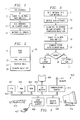
- the inventive error detection mechanism encodes messages as shown in FIGURE 1.
- the inventive mechanism allows the error correction code (ECC) (if any) to operate on the real data 11.
- ECC error correction code
- the mechanism treats the data bits and the associated ECC checkbits (if any) as its 'data' that it protects from wire stuck-at faults.
- the inventive mechanism counts 12 the number of 1's in the data part, i.e. the real data and checkbits, and stores the number as a counter value.
- the inventive mechanism can protect the counter value bits by adding ECC check bits 13 so that the counter value is protected with the same ECC scheme as in the data part.
- the inventive mechanism forms 14 a data message 20 comprising four parts: the real data part 21, the ECC check bits 22 protecting the real data, the counter value 23 with the number of 1's in the real data and its check bits, and check bits 24 protecting the counter value with the same ECC capability as the data part, as shown in FIGURE 2.
- the transmitted message is encoded with the real data, real data ECC, counter value, and counter value ECC.
- the message is then transmitted to the destination location via a transmission line or other transmission system.
- the invention has been described in terms of the ECC capabilities of the single-error correcting and double error-detecting (SEC-DED) code, the invention may work with any ECC code, including parity. Further note that although the invention has been described in terms of count 1's, the invention may also operate by counting 0's instead of counting 1's.
- a second instantiation of the inventive mechanism that is located at the destination of the message decodes the message as shown in FIGURE 3.
- the message is split into two sub-messages 31.
- the first sub-message comprises the real data and the real data ECC
- the second sub-message comprises the counter value and the counter value ECC.
- the first and second messages are then decoded separately according the ECC mechanism used for encoding 32. Any single bit errors in either the real data or the counter value would be detected and corrected via their respective ECC 33. Any double errors in either the real data or the counter value would be detected via their respective ECC 33. If a double error is found then the message is discarded and a resend or retry signal is sent to the originator of the message.
- wire failures can be detected.
- the inventive mechanism then counts the number of 1's in the decoded real data and real data ECC 34.
- the decoded counter value is then compared 35 with the counted number of 1's in the decoded real data plus the real data ECC check bits to determine if there is a wire stuck-at fault 36.
- any multiple errors, including malicious wire failures, that are present also are detected, unless offsetting multiple errors have occurred. Note that a malicious wire failure would be a wire that changes the transmitted values randomly. Offsetting multiple errors is where the number of 0 to 1 transitions equals the number of 1 to 0 transitions.
- An error is flagged 37 if the counter value does not match the number of 1's in the real data plus real data ECC. After a wire error is detected the data is considered corrupted. Different systems may invoke different error recovery mechanisms. Otherwise, no detectable error occurred during transmission of the message 38.
- the SEC-DED code requires 8 check bits, forming a (72, 64) ECC code. This code does not possess the capability to detect wire failures, which could introduce up to 5 errors. Note that the 72 bits would be sent over 17 wires, and thus at least one wire will be carrying 5 bits of the message, and if this wire fails, then up to 5 errors will occur. As the real data plus the real data ECC is 72 bits, then the real data plus real data ECC may have a total of 72 1's.
- the counter value will be a 7 bit value.
- the counter value itself will be protected by 5 bits of ECC forming a (12,7) SEC-DED ECC code.
- the message formed by inventive mechanism is 84 bits, 64 of which are real data.
- the message would be a (84,64) code.
- the encoded message is transmitted over 5 cycles through the channel (since the channel comprises 17 wires).
- the counter value is protected with the same ECC as the real data so that the overall message is guaranteed to be at the desired ECC (in this case the SEC-DED).
- ECC ECC
- the counter value is not protected with ECC.
- a single bit error in the counter value would cause a mismatch in the number of 1's with respect to the real data plus real data ECC. This mismatch would in turn cause an erroneous wire fault flag to be issued.
- a wire error could occur with an error pattern that escapes detection. For example, an error pattern due to a wire failure which introduces 4 total errors, with 3 errors in the 72 real data plus real data ECC bits and 1 error in the counter value.
- the (72, 64) ECC does not guarantee detection of 3 errors and may give a decoded bit pattern with 2 or 4 errors. With one of the bits in the counter changing, there may be a possibility that the erroneous data will pass through. It may also be possible for other error patterns along a wire failure to go undetected. Thus, protecting the counter value with some ECC prevents these problems from occurring.
- the counter value plus the counter value ECC should not exceed two bits on the same wire. For example, if there are 17 wires for transmission, then the counter value plus counter value ECC should not exceed 34 bits, assuming SEC-DED ECC. In other words, the counter value and the counter value ECC cannot be more than twice the wire width of the transmission channel. This restriction ensures that errors in the counter value due to a wire failure will be detected by the ECC. Thus, any single error in the counter value will be corrected, and any double errors in the counter value, either random or due to a wire failure, can be detected. Therefore, the counter value is protected with single error correction, double error detection, and wire failure detection.
- the restriction depends upon the type of ECC used, as type of ECC used affects the size of the message as well as the number of errors that can be detected. For example if single error detection (SED) ECC is used then the counter value plus counter value ECC should not exceed the wire size, as only single error can be detected, however the size of the ECC would be smaller as the number of bits for SED is less than SEC-DED. If the ECC being used on the real data is a parity bit, then it will be sufficient to protect the counter value with a parity bit, provided that the counter itself and the parity bit will protect against wire failure. In general terms, the size of the counter value plus counter value ECC should not exceed the size of the channel times the number of errors that can be detected by the ECC. Note that different types of ECC can be used. For example, the data may be protected with SEC-DED ECC, SED ECC, or double error correcting-triple error detecting ECC code, or any other types of ECC code.
- the inventive error detection mechanism can be reconfigured to accommodate situations where the counter value plus counter value ECC exceeds the above restrictions. For example, using the previously described (72,64) code the channel is 5 bits wide instead of 17 bits wide. The sub-message of the counter value and the counter value ECC is still 12 bits total and forms a (12, 7) code. Thus, two bits of the sub-message would be transmitted in a third cycle (i.e. 10 bits would be sent in the first two cycles). As three bits would be sent on at least one wire, then SEC-DED ECC could not guarantee the accuracy of the counter value.
- a first solution is to use multiple counters values, with each counter value having its own ECC check bits. For example, if the ECC is SEC-DED, then when the counter value and the counter value ECC check bits are more than twice the wire width, then a second counter value is formed by counting the number of 1's in the first counter value and its ECC check bits. The second counter value would then be appended with ECC check bits. This process will go on recursively until the last counter value and its ECC check bits are less than twice the wire width.
- the first counter value has (log k) bits, k being the number of information bits.
- the second counter value if required, will have (log (log k)) bits.
- FIGURE 5 depicts the first solution with the example above to form data packet message 50, that includes 72 data bits 51, d 0 ....d 71 , which includes SEC-DED ECC bits, and 12 first counter bits 52, C 0 ...C 11 , which includes SEC-DED ECC bits.
- a second counter is required.
- the second counter value holds the number of 1's in the first counter value, which needs to be 4 bits wide to hold the number of 1's in the 12 bit code.
- 4 bits of ECC are required.
- the second counter value and the second counter value ECC can be transmitted in less than three cycles, there is no need for a third counter. Note that this code forms a third sub-message, which would be decoded separately from the other two sub-messages. Therefore a total of 20 bits of counter value and counter value ECC would be appended to the real data and real data ECC.
- FIGURE 6 depicts the second solution with the example above to form data packet message 60, that includes 72 data bits 61, d 0 ....d 71 , which includes SEC-DED ECC bits, and 10 first counter bits 62, C 0 ...C 9 , which includes SEC-DED ECC bits.
- the counter value plus ECC 52 was 12 bits wide, however the total of size of the code can be up to 10 bits.
- FIGURE 7 depicts a message data protect 70 for the first solution with the 64 bit example, which includes 64 data bits 71, d 0 -d 63 , and parity bit Pd 72 for data bits 71.
- 65 bits being transmitted over 5 wires requires a counter with a width of 7 bits, C 0 -C 6 73. These 7 bits counter would be protected by another parity bit, a PC 74, requiring 8 bits.
- FIGURE 8 depicts a message data packet 80 for the second solution with the 64 data bit example, which includes 64 data bits 81, d 0 -d 63 , and parity bit Pd 82 for data bits 81.
- 64 data bit example which includes 64 data bits 81, d 0 -d 63 , and parity bit Pd 82 for data bits 81.
- the second solution divides the counter into multiple parts, with 5 wires the maximum size is 5 bits. Since 1 parity bit is required for protection, the counter is broken into segments no larger than 4 bits. Thus, 4 bits of the counter, C 0 -C 3 , 83 are protected with parity bit PCL 84, and 3 bits of the counter, C 4 -C 6 are protected with parity bit PCH 85. Note that the counters are shown as being segmented into 4 lower bits and 3 upper bits, however other divisions are possible. Note that the parity bits are unnecessary to detect single errors since the wire stuck at fault covers it. However they are used as an example since wire fault detection may not cover all types of ECC (e.g., SEC_DED).
- ECC e.g., SEC_DED
- a third solution is to reduce the size of the counter value, i.e. have a counter value that is less wide.
- the smaller the counter value then the smaller the sub-message.
- the smaller the counter value then the fewer the ECC bits that are required for protection, which in turn results in a smaller sub-message.
- a wire stuck at failure could only affect the counter by -5 (i.e. wire stuck at 0 and the real values are Is) through +5 (i.e. wire stuck at 1 and the real values are 0s).
- a counter of width 4 bits would have sufficed since it can tolerate a swing of 10.
- a (8, 4) SEC-DED ECC code 92, i.e. C 0 -C 7 is required to protect the counter value rather than the (12,7) code that is required for the earlier embodiment.
- the counter value should have width that is the upper ceiling of logarithm (base 2) of twice the number of cycles through which the entire code word is transmitted. Therefore, in this example, the number of 1's modulo 16 are being counted. This is performed by adding the 1's and doing a modulo operate while counting you may have the full width but while sending you chop off extra upper bits.
- the third solution is the preferred embodiment.
- the designer can also decide to have a lower number of counter value bits than required for a lower reliability, as a trade-off between detection and overhead (in terms of the number of check bits).
- the counter bits can be reduced a number below what is required to provide wire stuck at fault detection, but then wire stuck at fault detection can not be guaranteed.
- the counter value and the real data bits can be ECC protected together, if there is a shortage of check bits. However, this will not provide complete coverage against wire failures or stuck-at-faults. For example, suppose there is data and a counter with simple parity protection, and a wire failure occurs that changes 1 bit in the data and 1 bit in the counter (least significant bit). The parity will not detect the error and neither will the counter. Thus, in the above example, 4 bits for counter are required for 64 bits for data. To protect these 68 bits, 8 bits of ECC data are required, thus forming a (76, 68) SEC-DED ECC code.
- a single wire failure can be detected, however multiple wire failures may not be detected if the number of 0 to 1 transitions equals the number of 1 to 0 transitions. Thus, while some multiple wire failures may be detected, not all wire failures can be detected.
- the invention can operate in any data transmission environment that involves multiple wires and ECC is used, for example, between two computer connected via a LAN, WAN or Internet.
- the invention can also be used for data transmission within a computer system, e.g. between a RAM and CPU. This is particularly true for multi-processor systems.
- FIGURE 4 illustrates a computer system 400 adapted for use with the present invention.
- the wires that are used to send data bits could be the bus 402 or the bus linking 405-406 or the network 412.
- CPU central processing unit
- bus 402 is coupled to random access memory (RAM) 403, read only memory (ROM) 404, input/output (I/O) card 405, communications card 411, user interface card 408, and display card 409.
- RAM 403 and ROM 404 hold user and system data and programs as is well known in the art.
- I/O card 405 connects storage devices, such as hard drive 406, to the computer system.
- Communications card 411 is adapted to couple the computer system to a local, wide-area, or Internet network 412.
- User interface card 408 couples user input devices, such as keyboard 413 and pointing device 407, to the computer system 400.
- display card 409 is driven by CPU 401 to control the display on display device 410.
- CPU 401 may be any general purpose CPU, such as a HP PA-8200.
- the present invention is not restricted by the architecture of CPU 401 as long as CPU 401 supports the inventive operations as described herein.
- error code means correction and/or detection.
Applications Claiming Priority (2)
| Application Number | Priority Date | Filing Date | Title |
|---|---|---|---|
| US09/438,063 US6473877B1 (en) | 1999-11-10 | 1999-11-10 | ECC code mechanism to detect wire stuck-at faults |
| US438063 | 1999-11-10 |
Publications (2)
| Publication Number | Publication Date |
|---|---|
| EP1100205A2 true EP1100205A2 (de) | 2001-05-16 |
| EP1100205A3 EP1100205A3 (de) | 2001-10-10 |
Family
ID=23739054
Family Applications (1)
| Application Number | Title | Priority Date | Filing Date |
|---|---|---|---|
| EP00309866A Ceased EP1100205A3 (de) | 1999-11-10 | 2000-11-07 | Fehlerkode für Leitungsdefektdetektion |
Country Status (3)
| Country | Link |
|---|---|
| US (2) | US6473877B1 (de) |
| EP (1) | EP1100205A3 (de) |
| JP (1) | JP4053228B2 (de) |
Cited By (3)
| Publication number | Priority date | Publication date | Assignee | Title |
|---|---|---|---|---|
| EP1394559A1 (de) * | 2002-08-27 | 2004-03-03 | Siemens Aktiengesellschaft | Verfahren und Anordnung zur Erkennung und Behebung von Leitungsdefekten |
| EP1812866A1 (de) * | 2004-11-19 | 2007-08-01 | Samsung Electronics Co., Ltd. | Vorrichtung und verfahren zur verarbeitung der daten eines flash-speichers |
| US7613982B2 (en) | 2004-11-16 | 2009-11-03 | Samsung Electronics Co., Ltd. | Data processing apparatus and method for flash memory |
Families Citing this family (60)
| Publication number | Priority date | Publication date | Assignee | Title |
|---|---|---|---|---|
| US6473877B1 (en) | 1999-11-10 | 2002-10-29 | Hewlett-Packard Company | ECC code mechanism to detect wire stuck-at faults |
| US7096414B2 (en) * | 2003-08-04 | 2006-08-22 | Hewlett-Packard Development Company, L.P. | In-line wire error correction |
| JP3935149B2 (ja) * | 2004-01-16 | 2007-06-20 | 株式会社東芝 | 半導体集積回路 |
| JP4529714B2 (ja) * | 2005-02-09 | 2010-08-25 | 日本電気株式会社 | Dll回路サンプリングタイミング調整システム及びその方法並びにそれに用いる送受信装置 |
| US9288089B2 (en) | 2010-04-30 | 2016-03-15 | Ecole Polytechnique Federale De Lausanne (Epfl) | Orthogonal differential vector signaling |
| US9246713B2 (en) | 2010-05-20 | 2016-01-26 | Kandou Labs, S.A. | Vector signaling with reduced receiver complexity |
| US9985634B2 (en) | 2010-05-20 | 2018-05-29 | Kandou Labs, S.A. | Data-driven voltage regulator |
| US9077386B1 (en) | 2010-05-20 | 2015-07-07 | Kandou Labs, S.A. | Methods and systems for selection of unions of vector signaling codes for power and pin efficient chip-to-chip communication |
| US9564994B2 (en) * | 2010-05-20 | 2017-02-07 | Kandou Labs, S.A. | Fault tolerant chip-to-chip communication with advanced voltage |
| US9596109B2 (en) | 2010-05-20 | 2017-03-14 | Kandou Labs, S.A. | Methods and systems for high bandwidth communications interface |
| US9479369B1 (en) | 2010-05-20 | 2016-10-25 | Kandou Labs, S.A. | Vector signaling codes with high pin-efficiency for chip-to-chip communication and storage |
| US8593305B1 (en) | 2011-07-05 | 2013-11-26 | Kandou Labs, S.A. | Efficient processing and detection of balanced codes |
| US9288082B1 (en) | 2010-05-20 | 2016-03-15 | Kandou Labs, S.A. | Circuits for efficient detection of vector signaling codes for chip-to-chip communication using sums of differences |
| US9106220B2 (en) | 2010-05-20 | 2015-08-11 | Kandou Labs, S.A. | Methods and systems for high bandwidth chip-to-chip communications interface |
| US9251873B1 (en) | 2010-05-20 | 2016-02-02 | Kandou Labs, S.A. | Methods and systems for pin-efficient memory controller interface using vector signaling codes for chip-to-chip communications |
| US9667379B2 (en) | 2010-06-04 | 2017-05-30 | Ecole Polytechnique Federale De Lausanne (Epfl) | Error control coding for orthogonal differential vector signaling |
| FR2964222A1 (fr) * | 2010-08-25 | 2012-03-02 | Inst Telecom Telecom Bretagne | Dispositif d'apprentissage et de decodage de messages, mettant en œuvre un reseau de neurones, procedes d'apprentissage et de decodage et programmes d'ordinateur correspondants. |
| US9268683B1 (en) | 2012-05-14 | 2016-02-23 | Kandou Labs, S.A. | Storage method and apparatus for random access memory using codeword storage |
| CN104995612B (zh) | 2013-01-17 | 2020-01-03 | 康杜实验室公司 | 低同步开关噪声芯片间通信方法和系统 |
| KR102241045B1 (ko) | 2013-04-16 | 2021-04-19 | 칸도우 랩스 에스에이 | 고 대역폭 통신 인터페이스를 위한 방법 및 시스템 |
| EP2997704B1 (de) | 2013-06-25 | 2020-12-16 | Kandou Labs S.A. | Vektorsignalisierung mit reduzierter empfängerkomplexität |
| KR102098247B1 (ko) * | 2013-11-25 | 2020-04-08 | 삼성전자 주식회사 | 메모리 시스템에서 데이터를 인코딩 및 디코딩하기 위한 방법 및 장치 |
| US9806761B1 (en) | 2014-01-31 | 2017-10-31 | Kandou Labs, S.A. | Methods and systems for reduction of nearest-neighbor crosstalk |
| WO2015117102A1 (en) | 2014-02-02 | 2015-08-06 | Kandou Labs SA | Method and apparatus for low power chip-to-chip communications with constrained isi ratio |
| EP3111607B1 (de) | 2014-02-28 | 2020-04-08 | Kandou Labs SA | Vektorsignalisierungskodes mit eingebettetem takt |
| US9509437B2 (en) | 2014-05-13 | 2016-11-29 | Kandou Labs, S.A. | Vector signaling code with improved noise margin |
| US9148087B1 (en) | 2014-05-16 | 2015-09-29 | Kandou Labs, S.A. | Symmetric is linear equalization circuit with increased gain |
| US9852806B2 (en) | 2014-06-20 | 2017-12-26 | Kandou Labs, S.A. | System for generating a test pattern to detect and isolate stuck faults for an interface using transition coding |
| US9112550B1 (en) | 2014-06-25 | 2015-08-18 | Kandou Labs, SA | Multilevel driver for high speed chip-to-chip communications |
| KR102288337B1 (ko) | 2014-07-10 | 2021-08-11 | 칸도우 랩스 에스에이 | 증가한 신호대잡음 특징을 갖는 벡터 시그널링 코드 |
| US9432082B2 (en) | 2014-07-17 | 2016-08-30 | Kandou Labs, S.A. | Bus reversable orthogonal differential vector signaling codes |
| US9444654B2 (en) | 2014-07-21 | 2016-09-13 | Kandou Labs, S.A. | Multidrop data transfer |
| KR101949964B1 (ko) | 2014-08-01 | 2019-02-20 | 칸도우 랩스 에스에이 | 임베딩된 클록을 갖는 직교 차동 벡터 시그널링 코드 |
| US9674014B2 (en) | 2014-10-22 | 2017-06-06 | Kandou Labs, S.A. | Method and apparatus for high speed chip-to-chip communications |
| WO2016210445A1 (en) | 2015-06-26 | 2016-12-29 | Kandou Labs, S.A. | High speed communications system |
| US9557760B1 (en) | 2015-10-28 | 2017-01-31 | Kandou Labs, S.A. | Enhanced phase interpolation circuit |
| US9577815B1 (en) | 2015-10-29 | 2017-02-21 | Kandou Labs, S.A. | Clock data alignment system for vector signaling code communications link |
| US10055372B2 (en) | 2015-11-25 | 2018-08-21 | Kandou Labs, S.A. | Orthogonal differential vector signaling codes with embedded clock |
| EP3408935B1 (de) | 2016-01-25 | 2023-09-27 | Kandou Labs S.A. | Spannungssamplertreiber mit verbesserter hochfrequenzverstärkung |
| US10003454B2 (en) | 2016-04-22 | 2018-06-19 | Kandou Labs, S.A. | Sampler with low input kickback |
| EP3826184A1 (de) | 2016-04-22 | 2021-05-26 | Kandou Labs, S.A. | Hochleistungsphasenregelkreis |
| US10153591B2 (en) | 2016-04-28 | 2018-12-11 | Kandou Labs, S.A. | Skew-resistant multi-wire channel |
| EP3449606A4 (de) | 2016-04-28 | 2019-11-27 | Kandou Labs S.A. | Mehrstufiger treiber mit geringem stromverbrauch |
| CN109313622B (zh) | 2016-04-28 | 2022-04-15 | 康杜实验室公司 | 用于密集路由线组的向量信令码 |
| US9906358B1 (en) | 2016-08-31 | 2018-02-27 | Kandou Labs, S.A. | Lock detector for phase lock loop |
| US10411922B2 (en) | 2016-09-16 | 2019-09-10 | Kandou Labs, S.A. | Data-driven phase detector element for phase locked loops |
| US10200188B2 (en) | 2016-10-21 | 2019-02-05 | Kandou Labs, S.A. | Quadrature and duty cycle error correction in matrix phase lock loop |
| US10200218B2 (en) | 2016-10-24 | 2019-02-05 | Kandou Labs, S.A. | Multi-stage sampler with increased gain |
| US10372665B2 (en) | 2016-10-24 | 2019-08-06 | Kandou Labs, S.A. | Multiphase data receiver with distributed DFE |
| JP2018084947A (ja) | 2016-11-24 | 2018-05-31 | ルネサスエレクトロニクス株式会社 | 入出力システム、入力装置、入出力システムの制御方法 |
| CN110741562B (zh) | 2017-04-14 | 2022-11-04 | 康杜实验室公司 | 向量信令码信道的流水线式前向纠错 |
| US10116468B1 (en) | 2017-06-28 | 2018-10-30 | Kandou Labs, S.A. | Low power chip-to-chip bidirectional communications |
| US10686583B2 (en) | 2017-07-04 | 2020-06-16 | Kandou Labs, S.A. | Method for measuring and correcting multi-wire skew |
| US10693587B2 (en) | 2017-07-10 | 2020-06-23 | Kandou Labs, S.A. | Multi-wire permuted forward error correction |
| US10203226B1 (en) | 2017-08-11 | 2019-02-12 | Kandou Labs, S.A. | Phase interpolation circuit |
| US10908995B2 (en) | 2017-09-29 | 2021-02-02 | Nvidia Corporation | Securing against errors in an error correcting code (ECC) implemented in an automotive system |
| US10326623B1 (en) | 2017-12-08 | 2019-06-18 | Kandou Labs, S.A. | Methods and systems for providing multi-stage distributed decision feedback equalization |
| US10554380B2 (en) | 2018-01-26 | 2020-02-04 | Kandou Labs, S.A. | Dynamically weighted exclusive or gate having weighted output segments for phase detection and phase interpolation |
| US11356197B1 (en) | 2021-03-19 | 2022-06-07 | Kandou Labs SA | Error-tolerant forward error correction ordered set message decoder |
| CN116757158B (zh) * | 2023-08-11 | 2024-01-23 | 深圳致赢科技有限公司 | 基于半导体存储的数据管理方法 |
Family Cites Families (8)
| Publication number | Priority date | Publication date | Assignee | Title |
|---|---|---|---|---|
| US4701909A (en) * | 1986-07-24 | 1987-10-20 | American Telephone And Telegraph Company, At&T Bell Laboratories | Collision detection technique for an optical passive star local area network using CSMA/CD |
| US4965883A (en) * | 1988-08-24 | 1990-10-23 | Digital Equipment Corporation | Method and apparatus for transmitting and receiving characters using a balanced weight error correcting code |
| DE69228108T2 (de) * | 1991-10-29 | 1999-05-20 | Japan Broadcasting Corp | Verfahren und Vorrichtung zum Empfang von Informationssignalen |
| US6170073B1 (en) * | 1996-03-29 | 2001-01-02 | Nokia Mobile Phones (Uk) Limited | Method and apparatus for error detection in digital communications |
| US5996110A (en) * | 1996-12-16 | 1999-11-30 | Motorola, Inc. | Method and apparatus for decoding a data packet |
| US6084535A (en) * | 1997-01-30 | 2000-07-04 | Mitel Semiconductor Americas Inc. | System and method for generating many ones codes with hamming distance after precoding |
| US5892464A (en) * | 1997-03-19 | 1999-04-06 | Ericsson Inc. | Message encoding technique for communication systems |
| US6473877B1 (en) | 1999-11-10 | 2002-10-29 | Hewlett-Packard Company | ECC code mechanism to detect wire stuck-at faults |
-
1999
- 1999-11-10 US US09/438,063 patent/US6473877B1/en not_active Expired - Fee Related
-
2000
- 2000-10-26 JP JP2000327211A patent/JP4053228B2/ja not_active Expired - Fee Related
- 2000-11-07 EP EP00309866A patent/EP1100205A3/de not_active Ceased
-
2002
- 2002-09-17 US US10/245,260 patent/US6910169B2/en not_active Expired - Lifetime
Non-Patent Citations (2)
| Title |
|---|
| NN: "Checking Algorithm for Two Byte RAM with One or Two Byte Access" IBM TECHNICAL DISCLOSURE BULLETIN, vol. 37, no. 04B, April 1994 (1994-04), pages 655-657, XP002175029 * |
| T.R.N. RAO AND E. FUJIWARA: "Error-Control Coding for Computr Systems" , PRENTICE-HALL XP002175027 * page 48, line 1 - page 86, line 6 * * |
Cited By (6)
| Publication number | Priority date | Publication date | Assignee | Title |
|---|---|---|---|---|
| EP1394559A1 (de) * | 2002-08-27 | 2004-03-03 | Siemens Aktiengesellschaft | Verfahren und Anordnung zur Erkennung und Behebung von Leitungsdefekten |
| US7613982B2 (en) | 2004-11-16 | 2009-11-03 | Samsung Electronics Co., Ltd. | Data processing apparatus and method for flash memory |
| EP1812866A1 (de) * | 2004-11-19 | 2007-08-01 | Samsung Electronics Co., Ltd. | Vorrichtung und verfahren zur verarbeitung der daten eines flash-speichers |
| EP1812866A4 (de) * | 2004-11-19 | 2009-01-07 | Samsung Electronics Co Ltd | Vorrichtung und verfahren zur verarbeitung der daten eines flash-speichers |
| US8015344B2 (en) | 2004-11-19 | 2011-09-06 | Samsung Electronics Co., Ltd. | Apparatus and method for processing data of flash memory |
| US8230166B2 (en) | 2004-11-19 | 2012-07-24 | Samsung Electronics Co., Ltd. | Apparatus and method for processing data of flash memory |
Also Published As
| Publication number | Publication date |
|---|---|
| US20030066006A1 (en) | 2003-04-03 |
| JP4053228B2 (ja) | 2008-02-27 |
| US6910169B2 (en) | 2005-06-21 |
| JP2001211085A (ja) | 2001-08-03 |
| US6473877B1 (en) | 2002-10-29 |
| EP1100205A3 (de) | 2001-10-10 |
Similar Documents
| Publication | Publication Date | Title |
|---|---|---|
| US6473877B1 (en) | ECC code mechanism to detect wire stuck-at faults | |
| US7047475B2 (en) | CRC encoding scheme for conveying status information | |
| EP0136604B1 (de) | Dekodierverfahren und Vorrichtung dafür. | |
| US4796260A (en) | Schilling-Manela forward error correction and detection code method and apparatus | |
| US7730387B2 (en) | Data transmission method and apparatus using multiple scrambling codes | |
| EP1735795B1 (de) | Verfahren und vorrichtung zum schutz von teilen eines pakets in einem drahtlosen netzwerk | |
| US6473880B1 (en) | System and method for protecting data and correcting bit errors due to component failures | |
| US9787329B2 (en) | Efficient coding with single-error correction and double-error detection capabilities | |
| US7137057B2 (en) | Method and apparatus for performing error correction code (ECC) conversion | |
| US7080309B2 (en) | Multiple ECC schemes to improve bandwidth | |
| JPH0812612B2 (ja) | 誤り訂正方法及び装置 | |
| US6728920B1 (en) | Method for correcting errors in transfer of information | |
| JPS6346615B2 (de) | ||
| US7808917B2 (en) | Method and system for transmitting telegrams | |
| GB2216752A (en) | Forward error correction in packet switched communications | |
| WO2000073906A9 (en) | Mechanism for decoding linearly-shifted codes to facilitate correection of bit errors due to component failures | |
| CA2364072C (en) | Interconnect system with error correction | |
| EP1497926B1 (de) | Diversity-schema zur fehlerkontrollcodierung in einem system mit daten mit prioritäten | |
| EP3477478B1 (de) | Speicherarchitektur mit reaktionsmanager für fehlerkorrekturschaltung | |
| JP2732862B2 (ja) | データ伝送試験装置 | |
| CN109753369B (zh) | 一种寄存器及内存中顺序数组的数据编码及校验方法 | |
| US6886126B1 (en) | Apparatus and protocol for detected error propagation in serial-transport block-coded interfaces | |
| US5544179A (en) | Mis-synchronization detection system using a combined error correcting and cycle identifier code | |
| Lechner et al. | Methods for analysing and improving the fault resilience of delay-insensitive codes | |
| US6321357B1 (en) | Method and apparatus for burst error correction |
Legal Events
| Date | Code | Title | Description |
|---|---|---|---|
| PUAI | Public reference made under article 153(3) epc to a published international application that has entered the european phase |
Free format text: ORIGINAL CODE: 0009012 |
|
| AK | Designated contracting states |
Kind code of ref document: A2 Designated state(s): AT BE CH CY DE DK ES FI FR GB GR IE IT LI LU MC NL PT SE TR Kind code of ref document: A2 Designated state(s): DE FR GB |
|
| AX | Request for extension of the european patent |
Free format text: AL;LT;LV;MK;RO;SI |
|
| RIN1 | Information on inventor provided before grant (corrected) |
Inventor name: DAS SHARMA, DEBENDRA |
|
| PUAL | Search report despatched |
Free format text: ORIGINAL CODE: 0009013 |
|
| AK | Designated contracting states |
Kind code of ref document: A3 Designated state(s): AT BE CH CY DE DK ES FI FR GB GR IE IT LI LU MC NL PT SE TR |
|
| AX | Request for extension of the european patent |
Free format text: AL;LT;LV;MK;RO;SI |
|
| 17P | Request for examination filed |
Effective date: 20011126 |
|
| AKX | Designation fees paid |
Free format text: DE FR GB |
|
| 17Q | First examination report despatched |
Effective date: 20020617 |
|
| STAA | Information on the status of an ep patent application or granted ep patent |
Free format text: STATUS: THE APPLICATION HAS BEEN REFUSED |
|
| 18R | Application refused |
Effective date: 20060522 |