EP1098352A2 - Vorrichtung zur Bestimmung des Plasmaätz-Endpunktes und Verfahren - Google Patents
Vorrichtung zur Bestimmung des Plasmaätz-Endpunktes und Verfahren Download PDFInfo
- Publication number
- EP1098352A2 EP1098352A2 EP00309334A EP00309334A EP1098352A2 EP 1098352 A2 EP1098352 A2 EP 1098352A2 EP 00309334 A EP00309334 A EP 00309334A EP 00309334 A EP00309334 A EP 00309334A EP 1098352 A2 EP1098352 A2 EP 1098352A2
- Authority
- EP
- European Patent Office
- Prior art keywords
- plasma
- window portion
- semiconductor processing
- processing apparatus
- window
- Prior art date
- Legal status (The legal status is an assumption and is not a legal conclusion. Google has not performed a legal analysis and makes no representation as to the accuracy of the status listed.)
- Withdrawn
Links
Images


Classifications
-
- H—ELECTRICITY
- H10—SEMICONDUCTOR DEVICES; ELECTRIC SOLID-STATE DEVICES NOT OTHERWISE PROVIDED FOR
- H10P—GENERIC PROCESSES OR APPARATUS FOR THE MANUFACTURE OR TREATMENT OF DEVICES COVERED BY CLASS H10
- H10P72/00—Handling or holding of wafers, substrates or devices during manufacture or treatment thereof
- H10P72/06—Apparatus for monitoring, sorting, marking, testing or measuring
- H10P72/0604—Process monitoring, e.g. flow or thickness monitoring
-
- H—ELECTRICITY
- H01—ELECTRIC ELEMENTS
- H01J—ELECTRIC DISCHARGE TUBES OR DISCHARGE LAMPS
- H01J37/00—Discharge tubes with provision for introducing objects or material to be exposed to the discharge, e.g. for the purpose of examination or processing thereof
- H01J37/32—Gas-filled discharge tubes
- H01J37/32917—Plasma diagnostics
- H01J37/32935—Monitoring and controlling tubes by information coming from the object and/or discharge
-
- H—ELECTRICITY
- H10—SEMICONDUCTOR DEVICES; ELECTRIC SOLID-STATE DEVICES NOT OTHERWISE PROVIDED FOR
- H10P—GENERIC PROCESSES OR APPARATUS FOR THE MANUFACTURE OR TREATMENT OF DEVICES COVERED BY CLASS H10
- H10P72/00—Handling or holding of wafers, substrates or devices during manufacture or treatment thereof
- H10P72/04—Apparatus for manufacture or treatment
- H10P72/0402—Apparatus for fluid treatment
- H10P72/0418—Apparatus for fluid treatment for etching
- H10P72/0421—Apparatus for fluid treatment for etching for drying etching
Definitions
- the present invention relates to the field of semi-conductor wafer processing and, more particularly, to monitoring plasma etching.
- Plasma etching is a well known dry etching process in the art of semiconductor fabrication. It is also known that the endpoint of a plasma etching process may be determined by monitoring the level of emission of selected byproducts of the etching reaction. For example, an endpoint detector may be used for detecting byproducts of the etched layer in the exhaust stream of the etching chamber. The etching process is stopped when no more byproduct is detected.
- Endpoint detection may also rely on light emitted by the plasma during the etching reaction. This light includes emissions at wavelengths representative of specific substances present in the plasma. Therefore, the level of a reaction byproduct may be monitored through measurement of emissions at the byproduct's particular emission wavelength. By monitoring the level of a byproduct which originates from the layer being removed by the etching, the endpoint of the process is indicated by a sharp drop in the level of emitted reaction product. For example, in a plasma etching process wherein a layer of oxide is being removed, carbon monoxide (CO) is a typical byproduct released into the plasma. CO emits light at a wavelength of 483 nm. Therefore, when the oxide layer is fully removed, the CO emission decreases indicating the endpoint of the etch process.
- CO carbon monoxide
- the interference makes endpoint determination more difficult because an apparent drop in the emission being measured may be an artifact due to the modulation effect, rather than a true decrease indicating the endpoint of the etching process. This uncertainty causes an imprecise endpoint determination and contributes to reduced accuracy and quality control problems in the etching process.
- the apparatus includes a chamber having a window.
- the chamber has a substrate holder within for holding a semiconductor substrate.
- the chamber which is a plasma etching chamber, also includes a plasma generator for generating a plasma within the chamber.
- An optical fiber having opposing first and second ends, is positioned adjacent the window such that the first end is optically coupled to the plasma from outside the chamber. However, the optical fiber is positioned to avoid reflections from the semiconductor substrate.
- a processor is connected to the second end of the optical fiber for analyzing the plasma.
- the chamber window has a substantially planar portion and a substantially tubular portion extending outwardly therefrom.
- the tubular window portion has a closed end opposite the planar window portion.
- the first end of the optical fiber is connected to the closed end of the tubular window portion.
- the tubular window portion is positioned at a predetermined angle relative to the planar window portion so as to be optically coupled to view the plasma, while avoiding reflections from the semiconductor substrate to thereby eliminate the interference. Any angle sufficient to avoid reflections from the wafer may be employed in the apparatus, with an angle of about 60 from the planar window portion being a preferred angle.
- a method aspect of the invention for semiconductor processing includes generating a plasma within a chamber having a window, connecting an optical fiber to the window so as to be optically coupled to the plasma while avoiding reflections from the semiconductor substrate, and processing signals from the optical fiber for analysis of the plasma.
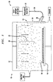
- FIG. 1 particularly illustrates in schematic view a semiconductor wafer processing apparatus 10 according to a preferred embodiment of the invention.
- the semiconductor processing apparatus 10 includes a chamber 12 having an opening with a window 14 therein.
- a substrate holder 16 is positioned within the chamber 12 for holding a semiconductor substrate 18 thereon.
- a plasma generator 20 is located within the chamber 12 for generating a plasma 22 adjacent the semiconductor substrate 18 .
- a remote plasma generator could also be used.
- An optical fiber 28 having opposing first and second ends has the first end positioned adjacent the window 14 such as to be optically coupled to the plasma 22 from outside the chamber 12 , while avoiding reflections from the semiconductor substrate 18 .
- a processor 30 is connected to the second end of the optical fiber 28 for analyzing the plasma.
- the processor 30 preferably includes a plasma etch endpoint detector configured for detecting a semiconductor processing byproduct serving to monitor the endpoint, for example CO.
- the window 14 includes a substantially planar window portion 24 and a substantially tubular window portion 26 extending outwardly therefrom.
- the window 14 is preferably a quartz window for allowing the transmission of light for analysis.
- the tubular window portion 26 has a closed end, and the first end of the optical fiber 28 is connected to the closed end of the tubular window portion 26 .
- the tubular window portion 26 is advantageously positioned at a predetermined angle relative to the planar window portion 24 so as to be optically coupled for viewing the plasma 22 , and to avoid reflections from the semiconductor substrate 18 .
- the predetermined angle may be varied according to requirements of the physical dimensions and structure of the surrounding apparatus, provided the tubular window portion 26 is set at an angle sufficient to exclude reflections from the semiconductor substrate 18 .
- the predetermined angle is about 60 relative to the plane of the planar window portion 24 , and is set so that the tubular window portion 26 is aimed toward an upper part of the chamber 12 .
- the window 14 may be positioned as practicable on the chamber 12 .
- a support bracket 34 is preferably included to secure the connection of the optical fiber 28 to the closed end of the tubular window portion 26 .
- the invention also preferably includes a wavelength selector 32 , also referred to as a monochromator, cooperating with the processor 30 .
- the wavelength selector 32 will be recognized by those skilled in the art to be any one of various devices for selecting the wavelength allowed to pass through for analysis.
- the wavelength selector 32 may be a wavelength filter, an interference filter such as a diffraction grating, or any other such device known in the art.
- the skilled artisan will additionally recognize that the wavelength selector 32 may be positioned relative to the apparatus anywhere practicable for selecting a wavelength for analysis.
- the wavelength selector 32 may be a component of the processor 30 , or it may be separate from the processor and positioned along the optical fiber 28 , or may even be connected between the closed end of the tubular window portion 26 and the first end of the optical fiber 28 .
- the wavelength selector 32 may be fixed to allow transmission of one or more predetermined wavelengths, or may be selectably adjustable to allow passage of one or more selected wavelengths.
- An additional aspect of the invention is directed to a method for semiconductor processing.
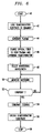
- the method includes the starting process step of loading a semiconductor substrate in the chamber (Block 42 ).
- a plasma is generated within a chamber having a window.
- an optical fiber is coupled adjacent the window such as to be optically coupled to the plasma from outside the chamber, but so as to avoid reflections from the semiconductor substrate.
- the method includes selecting a wavelength for monitoring (Block 48 ), and monitoring emission signals from the optical fiber (Block 50 ). If at Block 52 an endpoint determination is made during monitoring of emissions, then etching is terminated at Block 54 . Monitoring continues until an endpoint is determined. Upon termination of etching, the semiconductor substrate is unloaded from the chamber at Block 56 and the process stops at Block 58 .
Landscapes
- Physics & Mathematics (AREA)
- Engineering & Computer Science (AREA)
- Plasma & Fusion (AREA)
- Chemical & Material Sciences (AREA)
- Analytical Chemistry (AREA)
- Drying Of Semiconductors (AREA)
Applications Claiming Priority (2)
| Application Number | Priority Date | Filing Date | Title |
|---|---|---|---|
| US09/432,926 US6358359B1 (en) | 1999-11-03 | 1999-11-03 | Apparatus for detecting plasma etch endpoint in semiconductor fabrication and associated method |
| US432926 | 1999-11-03 |
Publications (1)
| Publication Number | Publication Date |
|---|---|
| EP1098352A2 true EP1098352A2 (de) | 2001-05-09 |
Family
ID=23718137
Family Applications (1)
| Application Number | Title | Priority Date | Filing Date |
|---|---|---|---|
| EP00309334A Withdrawn EP1098352A2 (de) | 1999-11-03 | 2000-10-23 | Vorrichtung zur Bestimmung des Plasmaätz-Endpunktes und Verfahren |
Country Status (2)
| Country | Link |
|---|---|
| US (1) | US6358359B1 (de) |
| EP (1) | EP1098352A2 (de) |
Cited By (1)
| Publication number | Priority date | Publication date | Assignee | Title |
|---|---|---|---|---|
| SG87924A1 (en) * | 2000-03-31 | 2002-04-16 | Applied Materials Inc | Monitoring a effluent from a chamber |
Families Citing this family (6)
| Publication number | Priority date | Publication date | Assignee | Title |
|---|---|---|---|---|
| EP1265278A1 (de) * | 2001-06-06 | 2002-12-11 | Infineon Technologies AG | Verfahren zur Herstellung eines Grabenkondensators mit Isolationsgraben |
| US6888639B2 (en) * | 2001-09-24 | 2005-05-03 | Applied Materials, Inc. | In-situ film thickness measurement using spectral interference at grazing incidence |
| US6930782B1 (en) * | 2003-03-28 | 2005-08-16 | Lam Research Corporation | End point detection with imaging matching in semiconductor processing |
| US7300594B2 (en) * | 2003-06-27 | 2007-11-27 | The Procter & Gamble Company | Process for purifying a lipophilic fluid by modifying the contaminants |
| US9997325B2 (en) * | 2008-07-17 | 2018-06-12 | Verity Instruments, Inc. | Electron beam exciter for use in chemical analysis in processing systems |
| KR102833984B1 (ko) | 2020-08-31 | 2025-07-15 | 삼성전자주식회사 | 반도체 장치 제조 공정의 모니터링 방법 및 이를 포함하는 반도체 장치의 제조 방법 |
Family Cites Families (8)
| Publication number | Priority date | Publication date | Assignee | Title |
|---|---|---|---|---|
| US5208644A (en) | 1990-05-18 | 1993-05-04 | Xinix, Inc. | Interference removal |
| US5499733A (en) | 1992-09-17 | 1996-03-19 | Luxtron Corporation | Optical techniques of measuring endpoint during the processing of material layers in an optically hostile environment |
| US5728253A (en) * | 1993-03-04 | 1998-03-17 | Tokyo Electron Limited | Method and devices for detecting the end point of plasma process |
| US5891352A (en) | 1993-09-16 | 1999-04-06 | Luxtron Corporation | Optical techniques of measuring endpoint during the processing of material layers in an optically hostile environment |
| KR0152355B1 (ko) * | 1994-03-24 | 1998-12-01 | 가나이 쓰토무 | 플라즈마 처리장치 및 처리방법 |
| JP3193265B2 (ja) | 1995-05-20 | 2001-07-30 | 東京エレクトロン株式会社 | プラズマエッチング装置 |
| US5846373A (en) | 1996-06-28 | 1998-12-08 | Lam Research Corporation | Method for monitoring process endpoints in a plasma chamber and a process monitoring arrangement in a plasma chamber |
| JPH11176815A (ja) * | 1997-12-15 | 1999-07-02 | Ricoh Co Ltd | ドライエッチングの終点判定方法およびドライエッチング装置 |
-
1999
- 1999-11-03 US US09/432,926 patent/US6358359B1/en not_active Expired - Lifetime
-
2000
- 2000-10-23 EP EP00309334A patent/EP1098352A2/de not_active Withdrawn
Cited By (1)
| Publication number | Priority date | Publication date | Assignee | Title |
|---|---|---|---|---|
| SG87924A1 (en) * | 2000-03-31 | 2002-04-16 | Applied Materials Inc | Monitoring a effluent from a chamber |
Also Published As
| Publication number | Publication date |
|---|---|
| US6358359B1 (en) | 2002-03-19 |
Similar Documents
| Publication | Publication Date | Title |
|---|---|---|
| USRE39145E1 (en) | Method and apparatus for in-situ monitoring of plasma etch and deposition processes using a pulsed broadband light source | |
| EP0735565B1 (de) | Verfahren und Gerät zur Überwachung des Trockenätzens eines dielektrischen Films bis zu einer gegebenen Dicke | |
| JP4925507B2 (ja) | スペクトル干渉法を用いる膜厚制御 | |
| US6745095B1 (en) | Detection of process endpoint through monitoring fluctuation of output data | |
| JPH0786254A (ja) | 半導体製造装置及び半導体製造方法 | |
| US20110090503A1 (en) | Apparatus for detecting arcs | |
| US6062729A (en) | Rapid IR transmission thermometry for wafer temperature sensing | |
| TWI758478B (zh) | 研磨裝置及研磨方法 | |
| WO2003027609A1 (en) | In-situ film thickness measurement using spectral interference at grazing incidence | |
| US5208644A (en) | Interference removal | |
| US20080078948A1 (en) | Processing termination detection method and apparatus | |
| WO1998058400A2 (en) | Liquid etch endpoint detection and process metrology | |
| US6358359B1 (en) | Apparatus for detecting plasma etch endpoint in semiconductor fabrication and associated method | |
| US8014891B2 (en) | Etching amount calculating method, storage medium, and etching amount calculating apparatus | |
| US10260868B2 (en) | Interferometric method and system using variable fringe spacing for inspecting transparent wafers for electronics, optics or optoelectronics | |
| US7227624B2 (en) | Method and apparatus for monitoring the condition of plasma equipment | |
| US6650426B1 (en) | Endpoint determination for recess etching to a precise depth | |
| JP2001194320A (ja) | 表面状態測定装置及び方法 | |
| US6750977B2 (en) | Apparatus for monitoring thickness of deposited layer in reactor and dry processing method | |
| US20040005727A1 (en) | Device and method for automatically determining the surface quality of a bonding interface between two wafers | |
| CN1554107A (zh) | 用于确定实时蚀刻速率的浅角干涉工艺及装置 | |
| TWI898234B (zh) | 用於半導體製程之光學儀器之故障檢測與操作就緒情況之系統及方法 | |
| JPH1064884A (ja) | エッチング装置及びエッチング方法 | |
| US6450683B1 (en) | Optical temperature measurement as an in situ monitor of etch rate | |
| JPH0518454B2 (de) |
Legal Events
| Date | Code | Title | Description |
|---|---|---|---|
| PUAI | Public reference made under article 153(3) epc to a published international application that has entered the european phase |
Free format text: ORIGINAL CODE: 0009012 |
|
| AK | Designated contracting states |
Kind code of ref document: A2 Designated state(s): AT BE CH CY DE DK ES FI FR GB GR IE IT LI LU MC NL PT SE |
|
| AX | Request for extension of the european patent |
Free format text: AL;LT;LV;MK;RO;SI |
|
| STAA | Information on the status of an ep patent application or granted ep patent |
Free format text: STATUS: THE APPLICATION IS DEEMED TO BE WITHDRAWN |
|
| 18D | Application deemed to be withdrawn |
Effective date: 20021101 |