EP1094514A2 - Shallow trench isolation structure for a bipolar transistor - Google Patents
Shallow trench isolation structure for a bipolar transistorInfo
- Publication number
- EP1094514A2 EP1094514A2 EP00122610A EP00122610A EP1094514A2 EP 1094514 A2 EP1094514 A2 EP 1094514A2 EP 00122610 A EP00122610 A EP 00122610A EP 00122610 A EP00122610 A EP 00122610A EP 1094514 A2 EP1094514 A2 EP 1094514A2
- Authority
- EP
- European Patent Office
- Prior art keywords
- annular
- region
- type
- semiconductor device
- isolation trench
- Prior art date
- Legal status (The legal status is an assumption and is not a legal conclusion. Google has not performed a legal analysis and makes no representation as to the accuracy of the status listed.)
- Granted
Links
Images









Classifications
-
- H—ELECTRICITY
- H10—SEMICONDUCTOR DEVICES; ELECTRIC SOLID-STATE DEVICES NOT OTHERWISE PROVIDED FOR
- H10D—INORGANIC ELECTRIC SEMICONDUCTOR DEVICES
- H10D10/00—Bipolar junction transistors [BJT]
- H10D10/40—Vertical BJTs
-
- H—ELECTRICITY
- H10—SEMICONDUCTOR DEVICES; ELECTRIC SOLID-STATE DEVICES NOT OTHERWISE PROVIDED FOR
- H10D—INORGANIC ELECTRIC SEMICONDUCTOR DEVICES
- H10D84/00—Integrated devices formed in or on semiconductor substrates that comprise only semiconducting layers, e.g. on Si wafers or on GaAs-on-Si wafers
- H10D84/01—Manufacture or treatment
- H10D84/0107—Integrating at least one component covered by H10D12/00 or H10D30/00 with at least one component covered by H10D8/00, H10D10/00 or H10D18/00, e.g. integrating IGFETs with BJTs
- H10D84/0109—Integrating at least one component covered by H10D12/00 or H10D30/00 with at least one component covered by H10D8/00, H10D10/00 or H10D18/00, e.g. integrating IGFETs with BJTs the at least one component covered by H10D12/00 or H10D30/00 being a MOS device
-
- H—ELECTRICITY
- H10—SEMICONDUCTOR DEVICES; ELECTRIC SOLID-STATE DEVICES NOT OTHERWISE PROVIDED FOR
- H10D—INORGANIC ELECTRIC SEMICONDUCTOR DEVICES
- H10D84/00—Integrated devices formed in or on semiconductor substrates that comprise only semiconducting layers, e.g. on Si wafers or on GaAs-on-Si wafers
- H10D84/01—Manufacture or treatment
- H10D84/0112—Integrating together multiple components covered by H10D8/00, H10D10/00 or H10D18/00, e.g. integrating multiple BJTs
-
- H—ELECTRICITY
- H10—SEMICONDUCTOR DEVICES; ELECTRIC SOLID-STATE DEVICES NOT OTHERWISE PROVIDED FOR
- H10D—INORGANIC ELECTRIC SEMICONDUCTOR DEVICES
- H10D84/00—Integrated devices formed in or on semiconductor substrates that comprise only semiconducting layers, e.g. on Si wafers or on GaAs-on-Si wafers
- H10D84/01—Manufacture or treatment
- H10D84/02—Manufacture or treatment characterised by using material-based technologies
- H10D84/03—Manufacture or treatment characterised by using material-based technologies using Group IV technology, e.g. silicon technology or silicon-carbide [SiC] technology
- H10D84/038—Manufacture or treatment characterised by using material-based technologies using Group IV technology, e.g. silicon technology or silicon-carbide [SiC] technology using silicon technology, e.g. SiGe
-
- H—ELECTRICITY
- H10—SEMICONDUCTOR DEVICES; ELECTRIC SOLID-STATE DEVICES NOT OTHERWISE PROVIDED FOR
- H10W—GENERIC PACKAGES, INTERCONNECTIONS, CONNECTORS OR OTHER CONSTRUCTIONAL DETAILS OF DEVICES COVERED BY CLASS H10
- H10W10/00—Isolation regions in semiconductor bodies between components of integrated devices
- H10W10/01—Manufacture or treatment
- H10W10/011—Manufacture or treatment of isolation regions comprising dielectric materials
- H10W10/014—Manufacture or treatment of isolation regions comprising dielectric materials using trench refilling with dielectric materials, e.g. shallow trench isolations
-
- H—ELECTRICITY
- H10—SEMICONDUCTOR DEVICES; ELECTRIC SOLID-STATE DEVICES NOT OTHERWISE PROVIDED FOR
- H10W—GENERIC PACKAGES, INTERCONNECTIONS, CONNECTORS OR OTHER CONSTRUCTIONAL DETAILS OF DEVICES COVERED BY CLASS H10
- H10W10/00—Isolation regions in semiconductor bodies between components of integrated devices
- H10W10/01—Manufacture or treatment
- H10W10/031—Manufacture or treatment of isolation regions comprising PN junctions
-
- H—ELECTRICITY
- H10—SEMICONDUCTOR DEVICES; ELECTRIC SOLID-STATE DEVICES NOT OTHERWISE PROVIDED FOR
- H10W—GENERIC PACKAGES, INTERCONNECTIONS, CONNECTORS OR OTHER CONSTRUCTIONAL DETAILS OF DEVICES COVERED BY CLASS H10
- H10W10/00—Isolation regions in semiconductor bodies between components of integrated devices
- H10W10/10—Isolation regions comprising dielectric materials
- H10W10/17—Isolation regions comprising dielectric materials formed using trench refilling with dielectric materials, e.g. shallow trench isolations
-
- H—ELECTRICITY
- H10—SEMICONDUCTOR DEVICES; ELECTRIC SOLID-STATE DEVICES NOT OTHERWISE PROVIDED FOR
- H10W—GENERIC PACKAGES, INTERCONNECTIONS, CONNECTORS OR OTHER CONSTRUCTIONAL DETAILS OF DEVICES COVERED BY CLASS H10
- H10W10/00—Isolation regions in semiconductor bodies between components of integrated devices
- H10W10/30—Isolation regions comprising PN junctions
Definitions
- the present invention relates to a semiconductor device having a shallow trench isolation (STI) structure and, more particularly, to a STI structure for isolation of bipolar transistors in a silicon semiconductor device.
- STI shallow trench isolation
- Bipolar transistors have a somewhat complicated structure and fabricated by a more complicated process compared to MOSFETs.
- the bipolar transistors however, have several advantages of higher operational speed, higher current driveability and low noise characteristic, and thus are used in a LSI as important constituent elements.
- a BiCMOS device wherein bipolar transistors and MOSFETs are integrated in a single chip has advantages of both the bipolar transistors and the CMOSFETs, and thus widely used in a variety of applications.
- Fig. 1 shows a conventional semiconductor device including bipolar transistors separated by a LOCOS technique
- Fig. 2 is a sectional view taken along line II-II in Fig. 1.
- the semiconductor device 100 is fabricated on a p-type silicon substrate (p-substrate) 102, and includes a pair of NPN bipolar transistors 104A and 104B, which are disposed in a plane symmetry with respect to a plane passing through the center of a p-well 122.
- Each of the pair of bipolar transistors 104A and 104B includes an n-well 107A or 107B constituting a collector region, a p-type intrinsic base region 108A or 108B disposed on the top portion of the n-well 107A or 107B, an n + -type emitter region 110A or 110B disposed on the intrinsic base region 108A or 108B, and a p + -type extrinsic base region 112A or 112B disposed on the intrinsic base region 108A or 108B adjacent to the emitter region 110A or 110B.
- n + -type collector contact region 114A or 114B is disposed in the top portion of the n-well 107A or 107B, and is electrically isolated from the extrinsic base region 112A or 112B by the LOCOS film 106.
- the intrinsic base region 108A or 108B, the emitter region 110A or 110B and the extrinsic base region 112A or 112B are electrically isolated from the collector contact region 114A or 114B by the LOCOS film 106.
- the extrinsic base region 112A or 112B, the emitter region 110A or 110B and the collector contact region 114A or 114B are provided with a base electrode 116A or 116B, an emitter electrode 118A or 118B and a collector electrode 120A or 120B, respectively.
- the base electrode 116A or 116B and the collector electrode 120A or 120B are made of silicide layers such as including CoSi 2 and TiSi 2
- the emitter electrode 118A or 118B has a two-layer structure including a polysilicon film 118a and a silicon oxide film 118b.
- a pair of side walls 118c made of silicon oxide film are disposed on respective side surfaces of the two-layer structure.
- the p-well 122 is disposed right under the LOCOS film 106 for encircling the n-well 107A or 107B and isolating the n-wells 107A and 107B from each other by using the isolation function of a p-n junction.
- bipolar transistors and MOSFETs are also requested to have finer patterns.
- This also requires a finer isolation structure, which the LOCOS technique cannot afford due to the presence of a bird's beak in the LOCOS film.
- a STI structure which is expected to meet the finer patterning is thus noticed in place of using the LOCOS structure.
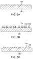
- Figs. 3A to 3F show a fabrication process for the STI structure in a semiconductor device.
- a thin SiO 2 film (not shown) is first formed on a silicon substrate 130, followed by deposition of a Si 3 N 4 film 132 thereon by a CVD technique.
- a photoresist film is formed on the Si 3 N 4 film 132 and subjected to patterning to form an etching mask 134 having openings for isolation trenches.
- the Si 3 N 4 film 132 is then etched using the etching mask 134 to form a Si 3 N 4 hard mask 136, as shown in Fig. 3B.
- the function of the thin SiO 2 film is to prevent damages from occurring on the main surface of the silicon substrate 130 due to the stress by the Si 3 N 4 film 132. Thereafter, the silicon substrate is subjected to a dry etching using the Si 3 N 4 hard mask 136 to form shallow isolation trenches 138, as shown in Fig. 3C.
- an insulator film for example, a SiO 2 film 140 is deposited on the entire surface including the surfaces of the hard mask 136 and the silicon substrate 130 to fill the shallow trenches 138, as shown in Fig. 3D.
- the insulator film may be a TEOS-SiO 2 film deposited by a TEOS-CVD technique.
- the SiO 2 film 140 is then subjected to a CMP process until the Si 3 N 4 hard mask 136 is exposed, as shown in Fig. 3E.
- the Si 3 N 4 film has a lower polishing rate compared to the SiO 2 film and thus functions as a stop layer for the polishing.
- the Si 3 N 4 hard mask 136 is then removed by etching to obtain the STI structure shown in Fig. 3F, wherein device areas are isolated from on another by the shallow isolation trenches 142.
- Consolidated LSIs wherein an analog signal circuit and a digital signal circuit are integrated in a single chip, are more and more used as the semiconductor devices for use in cellular phones etc.
- the area for the analog signal circuit has a fewer number of transistor elements compared to the area for the digital signal circuit.
- the transistor elements are more sparsely disposed in the analog circuit area compared to the transistor elements in the digital circuit area.
- the polishing rate of the CMP process generally depends on the density of the underlying pattern. More specifically, an area of the underlying pattern having a higher-density convex portions of the silicon substrate, which is not the subject area of the CMP process itself, has a lower polishing rate compared to another area of the underlying pattern having a lower-density convex portions of the silicon substrate.
- the isolation area of the silicon substrate having the lower-density convex portions due to the presence of a wider isolation trench therein may have a dishing portion (or depression) in the isolation area after the CMP process.
- the silicon substrate may have the dishing portion in the isolation area having a wider trench or lower-density concave portions. This causes a problem of an uneven top surface or a step of the silicon substrate, wherein the isolation area is lower than the device area which has higher-density convex portions.
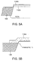
- Fig. 5A which shows the detail of the portion of the NPN bipolar transistor 104A
- the step formed by the dishing as described above resides between the wider shallow trench for the isolation area 106 and the device area for the bipolar transistor 104A. This causes an exposure of a part of the n-well 107A underlying the p + -type extrinsic base region 112A at the step after the removal of the silicon oxide film on the diffused region for formation of the silicide layer on the silicon substrate, as shown in Fig. 5A.
- the base electrode 116A may be in short-circuit with the n-well 107A if the height of the dishing portion is large. This applies to both the bipolar transistors 104A and 104B in Fig. 2, and degrades the yield rate of the products.
- the dishing portion may cause formation of a parasitic transistor at the step portion if the gate electrode extends from the device area along the step toward the dishing portion, as illustrated in Fig. 5B. This causes degradation of transistor characteristics of the MOSFET.
- the present invention provides a semiconductor device including a silicon substrate, and a bipolar transistor having a collector well having a first conductivity-type, an intrinsic having a second conductivity-type and received in the collector well and an emitter region having the first conductivity-type and received in the intrinsic base region, a first annular isolation trench encircling the collector well, a second annular isolation trench encircling the first annular isolation trench, and an annular diffused region disposed between the first annular isolation trench and the second isolation trench while being in contact with the first and second isolation trenches.
- the semiconductor device of the present invention by providing the first and second annular isolation trenches and annular diffused region sandwiched therebetween in an isolation area, the semiconductor device is free from a dishing portion in the isolation area due to high-density convex portions of the silicon substrate, whereby a transistor element isolated by the isolation area has excellent transistor characteristics.
- the second annular isolation trench may be associated with third and fourth annular isolation trenches, for example, encircling the second annular trench.
- annular trench as used herein means that a stripe trench is of an endless shape. It is not necessary that the outer or inner edge of the annular trench form a circle, and the outer or inner edge may form a rectangle or a square.
- the dishing portion is formed by the difference in the polishing rate which depends on the underlying pattern.
- the dishing portion is generally formed in the isolation area wherein the convex portions of the silicon substrate are sparse.
- the present inventor thus conceived that the isolation area should have higher-density convex portions, which can be achieved by providing a plurality of shallow trenches having a smaller width in a single isolation area, without increasing the occupied area for the isolation area.
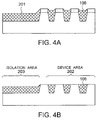
- Patent Publication JP-A-10-173035 describes a semiconductor device having isolation areas each formed by a plurality of shallow isolation trenches having a width equal to the width of the shallow isolation trenches formed in the device area for isolating adjacent transistor elements. Dummy diffused regions are formed between two of the shallow trenches in the isolation areas.
- the isolation area 203 includes three shallow trenches 204 and two dummy diffused regions 205 between each two of the shallow trenches 203.
- the shallow trench 204 in the isolation area 203 has a width equal to the width of the shallow isolation trench 204 disposed in the device area 202 for isolation of transistor elements (MOSFETs).
- MOSFETs transistor elements
- this STI structure has an advantage in that the density of the convex portions is equal between the device area 202 and the isolation area 203, and thus the dishing portion is not formed in the isolation area 203 after the CMP process.
- the dummy diffused region 205 has no specific function differently from the diffused regions 208 which constitute a MOSFET in association with a gate electrode 206.
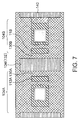
- the structure of Figs. 1 and 2 may be such that shown in Figs. 7 and 8.
- the wide LOCOS film 106 disposed between the collector contact regions 112A and 112B is replaced by a pair of shallow trenches 130A and 130B and a dummy diffused region 132 disposed therebetween.
- the top of the dummy diffused region 132 is covered by a silicide layer 134 which is formed during silicification for the base electrode etc.
- the dummy diffused regions 132 functions as a p-well for electrically isolating the n-wells 107A and 107B from each other.
- the present inventor conceived the STI structure for preventing the short-circuit failure. That is, the structure wherein the diffused region disposed between the first annular diffused region and the second annular diffused region is in contact with the first and second annular diffused regions prevents such a short-circuit failure even if a silicide layer is formed on the annular diffused region.
- the density of the convex portions of the silicon substrate is expressed by Wx100/S , wherein W is the area for the diffused region disposed between the first annular isolation trench and the second annular isolation trench, and S is the occupied area for an isolation area, i.e., the area between a first annular isolation trench of a first bipolar transistor and another first annular isolation trench of adjacent transistors.
- W is the area for the diffused region disposed between the first annular isolation trench and the second annular isolation trench
- S is the occupied area for an isolation area, i.e., the area between a first annular isolation trench of a first bipolar transistor and another first annular isolation trench of adjacent transistors.
- the pattern density have a higher value and a preferable pattern density is above 15%.
- the gap between adjacent two of the annular diffused regions is below 50 ⁇ m.
- Figs. 9 and 10 show a semiconductor device, generally designated by numeral 10, having a STI structure according to a first embodiment of the present invention.
- Fig. 10 illustrates a nMOSFET 14, a pMOSFET 16 and an NPN bipolar transistor 12, which are formed on a common p-type silicon substrate 18.
- Fig. 9 illustrates only the device area for the NPN bipolar transistor.
- the STI structure in the semiconductor device 10 includes a first annular isolation trench 20a and a second annular isolation trench 20b encircling the first annular isolation trench.
- Each of the annular isolation trenches has a structure wherein a trench formed on the surface region of the silicon substrate is filled with an insulator such as SiO 2 .
- the NPN bipolar transistor 12 is formed in a first area encircled by a first annular isolation trench 20a, which is encircled by a second annular isolation trench 20b.
- the CMOSFET including the nMOSFET and the pMOSFET is formed in a second area encircled by the second annular isolation trench 20b, with inner isolation trench 30 disposed inside the second annular isolation trench 20b.
- the width of the first and second annular isolation trenches 20a and 20b is preferably 0.1 to 10 ⁇ m depending on the layout of the transistor elements in the chip.
- the first annular isolation trench 20b for the NPN bipolar transistor 12 encircles an n-well or collector well 22 constituting the collector region of the NPN transistor 12.
- an annular p-well 21 is disposed between the first annular isolation trench 20a and the second annular isolation trench 20b for encircling the collector well 22.
- the p-well 12 functions for isolation by forming a p-n junction between the same and the collector well 22.
- the annular p-well 21 has an inner edge defined by the outer edge of the first annular isolation trench 20a and an outer edge defined by the inner edge of the second annular isolation trench 20b.
- the first region for the NPN bipolar transistor 12 defined by the first annular isolation trench 20a includes the n-type collector well 22, a p-type intrinsic base region 24 disposed on the top portion of the collector well 22, an n + -type emitter region 26 disposed on the intrinsic base region 24, and a p + -type extrinsic base region 28 disposed on the intrinsic base region 24 in the vicinity of the emitter region 26.
- the top edge portion of the collector well 22 is provided with an n + -type collector contact region 32, which is electrically isolated from the intrinsic base region 24, emitter region 26 and extrinsic base region 28 by an inner annular isolation trench 30 which is encircled by the first annular isolation trench 20a.
- the extrinsic base region 28, emitter region 36 and collector contact region 26 are provided with a base electrode 34, an emitter electrode 36 and a collector electrode 38, respectively.
- the base electrode 34 and the collector electrode 38 are made of silicide such as CoSi 2 or TiSi 2 .
- the emitter electrode 36 has a two-layer structure including a polysilicon film 36a and a silicon oxide film 36b, and also includes side walls 36c made of SiO 2 formed on the sides of the two-layer structure.
- a dummy silicide layer 39 is formed on the top of the p-well 21 between the first annular isolation trench 20a and the second annular isolation trench 20b concurrently with the silicide layer for the base electrode 34 and the collector electrode 38.
- the p-well 21 may have a p + -type top layer, on which the silicide layer 39 is formed.
- Each of the nMOSFET 14 and the pMOSFET 16 has a known LDD (lightly doped drain) structure and is formed in the device area isolated from the device area for the NPN bipolar transistor 12 by the first and second isolation trenchs 20a and 20b.
- LDD lightly doped drain
- the nMOSFET 14 includes a gate electrode 44 disposed on a p-well 40 with an intervention of a gate oxide film 42, and a pair of n + -type source/drain regions 46 formed in the surface region of the p-well 40 in the vicinity of the gate electrode 44.
- the gate electrode 44 has a two-layer structure including a polysilicon film 44a and an overlying silicide layer 44b, and includes side walls 44c formed on the sides of the two-layer structure.
- a pair of source/drain electrodes 47 made of silicide are formed on the source/drain regions 46.
- the pMOSFET 16 is isolated from the nMOSFET 14 by the inner isolation trench 30, and includes a gate electrode 50 disposed on an n-well 48 with an intervention of a gate oxide film 42 and a pair of p + -type source/drain regions 52 formed in the surface region of the n-well 48 in the vicinity of the gate electrode 50.
- the gate electrode 50 has a two layer structure including a polysilicon film 50a and an overlying silicide layer 50b, and includes side walls 50c on the sides of the tow-layer structure.
- a pair of source/drain electrodes 53 are formed on the respective source/drain regions 52.
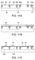
- the semiconductor device of the first embodiment is fabricated by the process shown in Figs. 11A to 11F.
- first annular isolation trenches 20a, second annular isolation trenches 20b and inner isolation trenches 30 are formed on the surface of the p-type silicon substrate 18, followed by ion implantation into the silicon substrate to form a p-well 21 between the first annular isolation trench 20a and the second annular isolation trench 20b, a p-well 40 in the device area for the nMOSFET 14, and an n-well 48 in the device are for the pMOSFET 16.
- the ion-implantation uses a known high-energy implantation technique, wherein phosphorous ions (n-type impurities) are introduced at an acceleration energy of 400 to 800 KeV and a dosage of 1x10 13 to 1x10 14 cm -2 , and wherein boron ions (p-type impurities) are introduced at an acceleration energy of 150 to 400 KeV and a dosage of 1x10 13 to 1x10 14 cm -2 .
- a 2- to 4-nm-thick gate oxide film 42 and a 10- to 25-nm-thick polysilicon film 56 are consecutively formed on the silicon substrate 18, as shown in Fig. 11B.
- an undoped amorphous silicon film or an amorphous silicon film doped with phosphorous, arsenic, or boron may be used instead of the polysilicon film.
- the polysilicon film 56 is subjected to patterning to form gate electrodes 44 and 50, followed by self-alignment ion-implantation steps to form n-type diffused regions 46a and p-type diffused regions 56a, which are aligned with the gate electrodes 44 and 50.
- phosphorous ions are implanted at an acceleration energy of 400 to 1000 KeV and a dosage of 1x10 13 to 1x10 14 cm -2 to form an n-well 22 in the device area for the NPN bipolar transistor 12, followed by implantation of boron (B) ions at an acceleration energy of several hundreds eV to 4 KeV and a dosage of 1x10 13 to 5x10 14 cm -2 , or alternatively BF2 at an acceleration energy of 1 to 15 KeV and a dosage of 1x10 13 to 5x10 14 cm -2 , to form an intrinsic base region 24.
- B boron
- a 20- to 80-nm-thick first LDD oxide film is formed on the entire surface of the substrate, followed by patterning thereof to form an opening 60 therein for exposing the emitter region.
- a 150- to 300-nm-thick polysilicon film is deposited and a 100- to 200-nm-thick silicon oxide film is grown thereon, followed by patterning of the polysilicon film 36a and the silicon oxide film 36b to form an emitter electrode 36.
- the polysilicon film may be replaced by an undoped amorphous silicon film or an amorphous film doped with phosphorous or arsenic.
- a 40- to 100-nm-thick second LDD oxide film (not shown) is formed on the entire surface of the substrate, followed by a known anisotropic etching to form side walls 44c and 50c on the sides of the gate electrodes 44 and 50, respectively, and side walls 36c on the sides of the emitter electrode 36, the side walls 44c and 50c of the gate electrodes including the first and second LDD oxide films, the side walls 36c including the second LDD oxide film.
- a heavily doped n-type diffused region 46, a heavily doped p-type diffused region 52 and a heavily doped p-type diffused region 28 are formed in a self-alignment with respect to the side walls 44c, 50c and 36c.
- a heavily doped n-type diffused region 32 is also formed.
- a rapid thermal annealing (RTA) step is conducted to diffuse the impurities in the polysilicon film 36a of the emitter electrode 36 toward the emitter region to form a heavily doped n-type region right under the polysilicon film 36a.
- Co cobalt
- the silicon of the substrate and the cobalt are reacted therebetween to form a CoSi 2 film, whereby CoSi 2 electrodes 47, 44a, 53, 50a, 34 and 38 are formed on the source/drain regions 46 and gate electrode 44 of the nMOSFET 14, source/drain regions and gate electrode of the pMOSFET 16, and the extrinsic base region 28 and collector contact region 32 of the NPN bipolar transistor, respectively.
- the combination of the first and second isolation trenches 20a and 20b together with the diffused region disposed therebetween constitutes an isolation area, which has a high-density convex portions of the substrate.
- CMP of the isolation area does not generate a dishing portion.
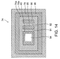
- a semiconductor device having a STI structure includes a pair of NPN bipolar transistors 72A and 72B disposed in symmetry with respect to a plane passing through the center of a p-well 21.
- the p-well 21 is disposed for isolation of the pair of NPN bipolar transistors 72A and 72B by forming a p-n junction between the same and the collector well 22 of each of the NPN bipolar transistors 72A and 72B.
- the configuration of each of the pair of NPN bipolar transistors 72A and 72B as well as the configuration of the isolation trenches 20a, 20b and 30 is similar to the configuration of those shown in Figs. 9 and 10.
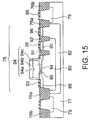
- a semiconductor device having a STI structure according to a third embodiment of the present invention is similar to the first embodiment except that a PNP transistor is formed in an n-well 82 encircled by a first annular isolation trench 76a, and that an inner isolation trench 92 is provided for isolation between the p-type collector region 80 and the n-well 82.
- the STI structure includes the first annular isolation trench 76a encircling the n-well 82, a second annular isolation trench 76b encircling the first annular isolation trench 76a, the inner isolation trenches 91 and 92.
- a p-well 79 is disposed between the first annular isolation trench 76a and the second annular isolation trench 76b for encircling the n-well 82 for isolation thereof.
- the n-well 82 receives therein the p-type collector well 80, an n-type intrinsic base region 84 formed on the top of the collector well 80, a p + -type emitter region 86 formed on the intrinsic base region 84, an n + -type extrinsic base region 88 formed on the intrinsic base region 84 adjacent to the emitter region 86, and a p + -type collector contact region 90 formed on the top periphery of the p-type collector region 80.
- the collector contact region 90 is isolated from the intrinsic base region 84, emitter region 86 and the extrinsic base region 88 by the inner isolation trench 91 which resides inside the first annular isolation trench 76a.
- the collector region 80 is isolated from the n-well 82 by the inner isolation trench 92 which resides inside the first annular isolation trench 76a.
- the extrinsic base region 88, emitter region 86 and collector contact region 90 are provided with a base electrode 93, an emitter electrode 94 and a collector electrode 95, respectively.
- the base electrode 93 and the collector electrode 95 are made of silicide such as CoSi 2 and TiSi 2 .
- the emitter electrode 94 has a two-layer structure including a polysilicon film 94a and a silicon oxide film 94b, and includes side walls 94c formed on the sides of the two-layer structure.
- a silicide film 96 is formed on the top of the p-type dummy well 79 between the first annular isolation trench 76a and the second annular isolation trench 76b concurrently with the silicide film formed on the base electrode 93 and the collector electrode 95.
- a similar silicide film 96 is formed on the top of the n-well 82.
- a semiconductor device having a STI structure according to a fourth embodiment of the present invention is similar to the first embodiment except for the structure of the isolation trenches for the NPN bipolar transistor.
- the semiconductor device of the present embodiment includes a first annular isolation trench 98a for encircling the n-type collector well of the NPN transistor 12, a second annular isolation trench 98b encircling the first annular isolation trench 98a, and a third annular isolation trench encircling the second annular isolation trench 98b.
- a plurality of first p-type diffused regions 99a are disposed between the first annular isolation trench 98a and the second annular isolation trench 98b for collectively forming an intermittent annular diffused region which encircles the collector well.
- a plurality of second p-type diffused regions 99b are disposed between the second annular isolation trench 98b and the third annular isolation trench 98c for collectively forming an intermittent annular diffused region.
- the intermittent diffused regions 99a and 99b have an isolation function by forming a p-n junction between the same and the n-type collector region.
- the first p-type diffused regions and the second p-type diffused regions are disposed alternatively as viewed along the annular diffused regions. In other words, any line extending in a radial direction, with the emitter region viewed as a center of a circle, passes inside the first p-type diffused regions 99a and/or the second p-type diffused regions 99b without fail.
- each of the intermittent annular diffused regions is replaced by a continuous annular diffused region.
- the isolation function of the isolation area can be improved.
Landscapes
- Element Separation (AREA)
- Bipolar Transistors (AREA)
- Metal-Oxide And Bipolar Metal-Oxide Semiconductor Integrated Circuits (AREA)
Abstract
Description
Claims (10)
- A semiconductor device comprising a silicon substrate (18), and a bipolar transistor (12) having a collector well (22) having a first conductivity-type, an intrinsic base region (24) having a second conductivity-type and received in said collector well (22) and an emitter region (26) having said first conductivity-type and received in said intrinsic base region (24), a first annular isolation trench (20a) encircling said collector well (22), a second annular isolation trench (20b) encircling said first annular isolation trench (20a), and an annular diffused region (21) disposed between said first annular isolation trench (20a) and said second annular isolation trench (20b) while being in contact with said first and second isolation trenches (20a, 20b).
- The semiconductor device as defined in claim 1, wherein said intrinsic base region (24) and said collector well (22) are provided with a base electrode (34) and a collector electrode (38), and each of said base electrode (34), said collector electrode (38) and said annular diffused region (21) is provided with a silicide layer on top thereof.
- The semiconductor device as defined in claim 1, further comprising a MOSFET (14, 16).
- The semiconductor device as defined in claim 1, wherein said annular diffused region includes a first intermittent annular sub-region including a plurality of first diffused regions (99a) and a second intermittent annular sub-region including a plurality of second diffused regions (99b), and said first diffused regions (99a) and said second diffused regions (99b) are arranged alternately along said annular diffused region.
- The semiconductor device as defined in claim 4, further comprising a third annular isolation trench (98b) disposed between said first intermittent annular region and said second intermittent annular region.
- The semiconductor device as defined in claim 6, wherein said silicon substrate (18) has said second conductivity-type.
- The semiconductor device as defined in claim 6, wherein said first conductivity-type is n-type and said second conductivity-type is p-type.
- The semiconductor device as defined in claim 6, wherein said silicon substrate (77) has said first conductivity-type, and includes a well (82) having said second conductivity-type and receiving therein said collector well (80).
- The semiconductor device as defined in claim 8, wherein said bipolar transistor (12) is a PNP transistor.
- The semiconductor device as defined in claim 1, further comprising a third annular isolation trench (98c) encircling said second annular isolation trench (98b), and another annular diffused region (99b) disposed between said second annular isolation trench (98b) and said third annular isolation trench (98c) while being in contact with said second and third annular isolation trenches (98b, 98c).
Applications Claiming Priority (2)
| Application Number | Priority Date | Filing Date | Title |
|---|---|---|---|
| JP29488599 | 1999-10-18 | ||
| JP29488599A JP3748744B2 (en) | 1999-10-18 | 1999-10-18 | Semiconductor device |
Publications (3)
| Publication Number | Publication Date |
|---|---|
| EP1094514A2 true EP1094514A2 (en) | 2001-04-25 |
| EP1094514A3 EP1094514A3 (en) | 2004-12-15 |
| EP1094514B1 EP1094514B1 (en) | 2007-08-29 |
Family
ID=17813518
Family Applications (1)
| Application Number | Title | Priority Date | Filing Date |
|---|---|---|---|
| EP00122610A Expired - Lifetime EP1094514B1 (en) | 1999-10-18 | 2000-10-17 | Shallow trench isolation structure for a bipolar transistor |
Country Status (4)
| Country | Link |
|---|---|
| US (1) | US6737721B1 (en) |
| EP (1) | EP1094514B1 (en) |
| JP (1) | JP3748744B2 (en) |
| DE (1) | DE60036177T2 (en) |
Cited By (5)
| Publication number | Priority date | Publication date | Assignee | Title |
|---|---|---|---|---|
| WO2002021581A3 (en) * | 2000-09-05 | 2002-08-15 | Motorola Inc | Method for uniform polish microelectronic device |
| WO2002091463A1 (en) * | 2001-05-04 | 2002-11-14 | Infineon Technologies Ag | Semiconductor process and integrated circuit |
| WO2002097895A3 (en) * | 2001-05-26 | 2003-09-25 | Ihp Gmbh | Transistor, method for producing an integrated circuit and method for producing a metal silicide layer |
| WO2006114753A3 (en) * | 2005-04-28 | 2008-04-03 | Nxp Bv | Method of fabricating a bipolar transistor |
| CN110391226A (en) * | 2018-04-18 | 2019-10-29 | 瑞萨电子株式会社 | Semiconductor devices |
Families Citing this family (6)
| Publication number | Priority date | Publication date | Assignee | Title |
|---|---|---|---|---|
| JP3621359B2 (en) | 2001-05-25 | 2005-02-16 | Necエレクトロニクス株式会社 | Semiconductor device and manufacturing method thereof |
| US7084485B2 (en) * | 2003-12-31 | 2006-08-01 | Freescale Semiconductor, Inc. | Method of manufacturing a semiconductor component, and semiconductor component formed thereby |
| KR101118652B1 (en) * | 2004-12-17 | 2012-03-07 | 삼성전자주식회사 | Bipolar Junction Transistor with high Gain integratable with CMOS FET process and Method for Forming the Same |
| US8461621B2 (en) * | 2010-03-09 | 2013-06-11 | Taiwan Semiconductor Manufacturing Company, Ltd. | Method and apparatus of forming bipolar transistor device |
| KR101717548B1 (en) * | 2010-04-09 | 2017-03-17 | 삼성전자 주식회사 | Semiconductor devices and method of fabricating the same |
| CN105810727B (en) * | 2014-12-30 | 2019-01-22 | 展讯通信(上海)有限公司 | a bipolar transistor |
Family Cites Families (25)
| Publication number | Priority date | Publication date | Assignee | Title |
|---|---|---|---|---|
| JPS5120267B2 (en) * | 1972-05-13 | 1976-06-23 | ||
| JPS5235582A (en) | 1975-09-13 | 1977-03-18 | Toshiba Corp | Transistor |
| JPS61230333A (en) * | 1985-04-05 | 1986-10-14 | Nec Corp | Integrated circuit |
| US4753901A (en) * | 1985-11-15 | 1988-06-28 | Ncr Corporation | Two mask technique for planarized trench oxide isolation of integrated devices |
| DE3883459T2 (en) | 1987-07-29 | 1994-03-17 | Fairchild Semiconductor | Method of manufacturing complementary contactless vertical bipolar transistors. |
| JPH01290235A (en) | 1988-05-17 | 1989-11-22 | Iwatsu Electric Co Ltd | Semiconductor integrated circuit device |
| JPH0222857A (en) | 1988-07-11 | 1990-01-25 | Nec Corp | Manufacture of semiconductor device |
| JPH0226062A (en) | 1988-07-14 | 1990-01-29 | Matsushita Electron Corp | Manufacturing method of semiconductor integrated circuit |
| JPH0294564A (en) * | 1988-09-30 | 1990-04-05 | Toshiba Corp | Manufacture of semiconductor device |
| JPH02151050A (en) | 1988-12-01 | 1990-06-11 | Nec Corp | semiconductor equipment |
| JPH0353561A (en) | 1989-07-21 | 1991-03-07 | Fujitsu Ltd | Semiconductor integrated circuit device |
| JPH05251653A (en) | 1992-03-04 | 1993-09-28 | Hitachi Ltd | Semiconductor integrated circuit device and manufacturing method thereof |
| JPH0621365A (en) | 1992-06-29 | 1994-01-28 | Toshiba Corp | Semiconductor integrated circuit device and manufacture thereof |
| JPH0737892A (en) | 1993-07-23 | 1995-02-07 | Toshiba Corp | Semiconductor integrated circuit device |
| KR950021600A (en) * | 1993-12-09 | 1995-07-26 | 가나이 쯔또무 | Semiconductor integrated circuit device and manufacturing method thereof |
| JPH0992658A (en) | 1995-09-20 | 1997-04-04 | Nec Corp | Semiconductor device and method of manufacturing semiconductor device |
| JPH09115998A (en) | 1995-10-16 | 1997-05-02 | Toshiba Corp | Element isolation structure of semiconductor integrated circuit and element isolation method |
| JP3326088B2 (en) * | 1996-03-14 | 2002-09-17 | 株式会社東芝 | Semiconductor device and manufacturing method thereof |
| US6030864A (en) * | 1996-04-12 | 2000-02-29 | Texas Instruments Incorporated | Vertical NPN transistor for 0.35 micrometer node CMOS logic technology |
| JPH10173035A (en) | 1996-12-10 | 1998-06-26 | Hitachi Ltd | Semiconductor integrated circuit device and its design method |
| JP3077742B2 (en) | 1997-03-03 | 2000-08-14 | 日本電気株式会社 | Semiconductor device and manufacturing method thereof |
| JP3189743B2 (en) | 1997-06-26 | 2001-07-16 | 日本電気株式会社 | Semiconductor integrated circuit device and method of manufacturing the same |
| JP3196714B2 (en) | 1998-03-05 | 2001-08-06 | 日本電気株式会社 | Manufacturing method of semiconductor integrated circuit having triple well structure |
| US6150697A (en) * | 1998-04-30 | 2000-11-21 | Denso Corporation | Semiconductor apparatus having high withstand voltage |
| US6355537B1 (en) * | 1999-02-23 | 2002-03-12 | Silicon Wave, Inc. | Method of providing radio frequency isolation of device mesas using guard ring regions within an integrated circuit device |
-
1999
- 1999-10-18 JP JP29488599A patent/JP3748744B2/en not_active Expired - Fee Related
-
2000
- 2000-10-17 DE DE60036177T patent/DE60036177T2/en not_active Expired - Fee Related
- 2000-10-17 EP EP00122610A patent/EP1094514B1/en not_active Expired - Lifetime
- 2000-10-18 US US09/691,456 patent/US6737721B1/en not_active Expired - Lifetime
Cited By (8)
| Publication number | Priority date | Publication date | Assignee | Title |
|---|---|---|---|---|
| WO2002021581A3 (en) * | 2000-09-05 | 2002-08-15 | Motorola Inc | Method for uniform polish microelectronic device |
| US6770929B2 (en) | 2000-09-05 | 2004-08-03 | Freescale Semiconductor, Inc. | Method for uniform polish in microelectronic device |
| WO2002091463A1 (en) * | 2001-05-04 | 2002-11-14 | Infineon Technologies Ag | Semiconductor process and integrated circuit |
| WO2002097895A3 (en) * | 2001-05-26 | 2003-09-25 | Ihp Gmbh | Transistor, method for producing an integrated circuit and method for producing a metal silicide layer |
| US7196382B2 (en) | 2001-05-26 | 2007-03-27 | Ihp Gmbh Innovations For High Performance Microelectronics/ Institut Fur Innovative Mikroelektronik | Transistor, method for producing an integrated circuit and a method of producing a metal silicide layer |
| WO2006114753A3 (en) * | 2005-04-28 | 2008-04-03 | Nxp Bv | Method of fabricating a bipolar transistor |
| CN110391226A (en) * | 2018-04-18 | 2019-10-29 | 瑞萨电子株式会社 | Semiconductor devices |
| CN110391226B (en) * | 2018-04-18 | 2024-05-31 | 瑞萨电子株式会社 | Semiconductor device |
Also Published As
| Publication number | Publication date |
|---|---|
| EP1094514B1 (en) | 2007-08-29 |
| JP3748744B2 (en) | 2006-02-22 |
| DE60036177D1 (en) | 2007-10-11 |
| US6737721B1 (en) | 2004-05-18 |
| JP2001118858A (en) | 2001-04-27 |
| EP1094514A3 (en) | 2004-12-15 |
| DE60036177T2 (en) | 2008-05-15 |
Similar Documents
| Publication | Publication Date | Title |
|---|---|---|
| EP0375585B1 (en) | Method for manufacturing a BI-CMOS device | |
| US6445044B2 (en) | Apparatus improving latchup immunity in a dual-polysilicon gate | |
| JP3888658B2 (en) | Semiconductor device having SOI structure and manufacturing method thereof | |
| CN101887911B (en) | Lateral bipolar junction transistor and method of manufacturing the same | |
| US5001073A (en) | Method for making bipolar/CMOS IC with isolated vertical PNP | |
| US5124271A (en) | Process for fabricating a BiCMOS integrated circuit | |
| JPH058583B2 (en) | ||
| US5943564A (en) | BiCMOS process for forming double-poly MOS and bipolar transistors with substantially identical device architectures | |
| US20060226488A1 (en) | Lateral bipolar transistor with additional ESD implant | |
| EP1094514B1 (en) | Shallow trench isolation structure for a bipolar transistor | |
| US6211001B1 (en) | Electrostatic discharge protection for salicided devices and method of making same | |
| US5395789A (en) | Integrated circuit with self-aligned isolation | |
| US6692998B2 (en) | Integrated high quality diode | |
| US5929506A (en) | Isolated vertical PNP transistor and methods for making same in a digital BiCMOS process | |
| US7138313B2 (en) | Method for creating a self-aligned SOI diode by removing a polysilicon gate during processing | |
| JPH11330269A (en) | Twin well formation method | |
| US5994190A (en) | Semiconductor device with impurity layer as channel stopper immediately under silicon oxide film | |
| US6933203B2 (en) | Methods for improving well to well isolation | |
| US5880002A (en) | Method for making isolated vertical PNP transistor in a digital BiCMOS process | |
| JP3244412B2 (en) | Semiconductor integrated circuit | |
| JPH08330440A (en) | Silicon-on-insulator semiconductor device | |
| US5141884A (en) | Isolation method of semiconductor device | |
| JPH0492466A (en) | Semiconductor device and manufacture thereof | |
| US5451530A (en) | Method for forming integrated circuits having buried doped regions | |
| US5310690A (en) | Method for forming integrated circuits having buried doped regions |
Legal Events
| Date | Code | Title | Description |
|---|---|---|---|
| PUAI | Public reference made under article 153(3) epc to a published international application that has entered the european phase |
Free format text: ORIGINAL CODE: 0009012 |
|
| AK | Designated contracting states |
Kind code of ref document: A2 Designated state(s): AT BE CH CY DE DK ES FI FR GB GR IE IT LI LU MC NL PT SE |
|
| AX | Request for extension of the european patent |
Free format text: AL;LT;LV;MK;RO;SI |
|
| RAP1 | Party data changed (applicant data changed or rights of an application transferred) |
Owner name: NEC ELECTRONICS CORPORATION |
|
| PUAL | Search report despatched |
Free format text: ORIGINAL CODE: 0009013 |
|
| AK | Designated contracting states |
Kind code of ref document: A3 Designated state(s): AT BE CH CY DE DK ES FI FR GB GR IE IT LI LU MC NL PT SE |
|
| AX | Request for extension of the european patent |
Extension state: AL LT LV MK RO SI |
|
| 17P | Request for examination filed |
Effective date: 20041116 |
|
| 17Q | First examination report despatched |
Effective date: 20050309 |
|
| AKX | Designation fees paid |
Designated state(s): DE |
|
| 17Q | First examination report despatched |
Effective date: 20050309 |
|
| GRAP | Despatch of communication of intention to grant a patent |
Free format text: ORIGINAL CODE: EPIDOSNIGR1 |
|
| GRAS | Grant fee paid |
Free format text: ORIGINAL CODE: EPIDOSNIGR3 |
|
| GRAA | (expected) grant |
Free format text: ORIGINAL CODE: 0009210 |
|
| AK | Designated contracting states |
Kind code of ref document: B1 Designated state(s): DE |
|
| REF | Corresponds to: |
Ref document number: 60036177 Country of ref document: DE Date of ref document: 20071011 Kind code of ref document: P |
|
| PLBE | No opposition filed within time limit |
Free format text: ORIGINAL CODE: 0009261 |
|
| STAA | Information on the status of an ep patent application or granted ep patent |
Free format text: STATUS: NO OPPOSITION FILED WITHIN TIME LIMIT |
|
| 26N | No opposition filed |
Effective date: 20080530 |
|
| PGFP | Annual fee paid to national office [announced via postgrant information from national office to epo] |
Ref country code: DE Payment date: 20081014 Year of fee payment: 9 |
|
| PG25 | Lapsed in a contracting state [announced via postgrant information from national office to epo] |
Ref country code: DE Free format text: LAPSE BECAUSE OF NON-PAYMENT OF DUE FEES Effective date: 20100501 |