EP1094487A2 - Wechselstrom-Plasmaanzeigevorrichtung - Google Patents
Wechselstrom-Plasmaanzeigevorrichtung Download PDFInfo
- Publication number
- EP1094487A2 EP1094487A2 EP00122987A EP00122987A EP1094487A2 EP 1094487 A2 EP1094487 A2 EP 1094487A2 EP 00122987 A EP00122987 A EP 00122987A EP 00122987 A EP00122987 A EP 00122987A EP 1094487 A2 EP1094487 A2 EP 1094487A2
- Authority
- EP
- European Patent Office
- Prior art keywords
- electrodes
- display
- front substrate
- barrier
- discharge
- Prior art date
- Legal status (The legal status is an assumption and is not a legal conclusion. Google has not performed a legal analysis and makes no representation as to the accuracy of the status listed.)
- Withdrawn
Links
Images


Classifications
-
- H—ELECTRICITY
- H01—ELECTRIC ELEMENTS
- H01J—ELECTRIC DISCHARGE TUBES OR DISCHARGE LAMPS
- H01J11/00—Gas-filled discharge tubes with alternating current induction of the discharge, e.g. alternating current plasma display panels [AC-PDP]; Gas-filled discharge tubes without any main electrode inside the vessel; Gas-filled discharge tubes with at least one main electrode outside the vessel
- H01J11/20—Constructional details
- H01J11/34—Vessels, containers or parts thereof, e.g. substrates
- H01J11/36—Spacers, barriers, ribs, partitions or the like
-
- H—ELECTRICITY
- H01—ELECTRIC ELEMENTS
- H01J—ELECTRIC DISCHARGE TUBES OR DISCHARGE LAMPS
- H01J11/00—Gas-filled discharge tubes with alternating current induction of the discharge, e.g. alternating current plasma display panels [AC-PDP]; Gas-filled discharge tubes without any main electrode inside the vessel; Gas-filled discharge tubes with at least one main electrode outside the vessel
- H01J11/10—AC-PDPs with at least one main electrode being out of contact with the plasma
- H01J11/12—AC-PDPs with at least one main electrode being out of contact with the plasma with main electrodes provided on both sides of the discharge space
-
- H—ELECTRICITY
- H01—ELECTRIC ELEMENTS
- H01J—ELECTRIC DISCHARGE TUBES OR DISCHARGE LAMPS
- H01J11/00—Gas-filled discharge tubes with alternating current induction of the discharge, e.g. alternating current plasma display panels [AC-PDP]; Gas-filled discharge tubes without any main electrode inside the vessel; Gas-filled discharge tubes with at least one main electrode outside the vessel
- H01J11/20—Constructional details
- H01J11/22—Electrodes, e.g. special shape, material or configuration
- H01J11/24—Sustain electrodes or scan electrodes
-
- H—ELECTRICITY
- H01—ELECTRIC ELEMENTS
- H01J—ELECTRIC DISCHARGE TUBES OR DISCHARGE LAMPS
- H01J11/00—Gas-filled discharge tubes with alternating current induction of the discharge, e.g. alternating current plasma display panels [AC-PDP]; Gas-filled discharge tubes without any main electrode inside the vessel; Gas-filled discharge tubes with at least one main electrode outside the vessel
- H01J11/20—Constructional details
- H01J11/22—Electrodes, e.g. special shape, material or configuration
- H01J11/32—Disposition of the electrodes
-
- H—ELECTRICITY
- H01—ELECTRIC ELEMENTS
- H01J—ELECTRIC DISCHARGE TUBES OR DISCHARGE LAMPS
- H01J11/00—Gas-filled discharge tubes with alternating current induction of the discharge, e.g. alternating current plasma display panels [AC-PDP]; Gas-filled discharge tubes without any main electrode inside the vessel; Gas-filled discharge tubes with at least one main electrode outside the vessel
- H01J11/20—Constructional details
- H01J11/34—Vessels, containers or parts thereof, e.g. substrates
- H01J11/42—Fluorescent layers
-
- H—ELECTRICITY
- H01—ELECTRIC ELEMENTS
- H01J—ELECTRIC DISCHARGE TUBES OR DISCHARGE LAMPS
- H01J2211/00—Plasma display panels with alternate current induction of the discharge, e.g. AC-PDPs
- H01J2211/20—Constructional details
- H01J2211/22—Electrodes
- H01J2211/32—Disposition of the electrodes
- H01J2211/323—Mutual disposition of electrodes
Definitions
- the present invention relates to an AC plasma display device used for a television receiver, an advertising display panel, and other image displays.
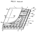
- FIG. 9 illustrates a main structure of a conventional AC plasma display device.
- a scan electrode 4 and sustain electrode 5 form a pair, which refers simply to display electrode, in a stripe shape.
- a plurality of the pairs is arranged in parallel on front substrate 1 and covered by dielectric layer 2 and protect film 3.
- Light shielding layer 6 is located between adjacent display electrodes (pairs of scan electrode 4 and sustain electrode 5).
- Scan electrode 4 and sustain electrode 5 are composed of transparent electrodes 4a and 5a and bus lines 4b and 5b respectively.
- the bus lines are made of silver and the like, and are stick to and electrically connected to the transparent electrodes respectively.
- a plurality of data electrodes 9 covered by insulating layer 8 is arranged on rear substrate 7.
- a plurality of partitions 10 is on insulating layer 8. Each one of partitions 10 is located in parallel with and between adjacent data electrodes 9.
- Phosphor 11 is coated on side partitions 10a and a surface of insulating layer 8 which are between partitions 10 adjacent to data electrode 9.
- Rear substrate 7 and front substrate 1 are placed facing to each other so that data electrodes 9 and the display electrodes extend in an perpendicular direction to each other, and define discharge spaces 12, where the display electrode include scan electrode 4 and sustain electrode 5.
- Discharge spaces 12 enclose helium, neon, argon, and xenon or a mixture of some of them as an ionizable gas.
- the display electrode composed of scan electrode 4 and sustain electrode 5 and data electrode 9 are arranged to form an intersection region between themselves, and the intersection region corresponds to one discharge cell.
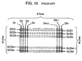
- FIG. 10 shows that arrays of electrodes of this display panel form a matrix structure of discharge cells with M lines and N rows, and the M lines have scan electrodes SCN1 through SCNM and sustain electrodes SUS1through SUSM in the line direction, the N rows have data electrodes D1 through DN in the row direction.
- FIG. 11 shows a timing chart illustrating a driving method of this AC plasma display panel
- FIGs. 10 and 11 illustrate the following.
- a positive write pulse voltage +V w volts is applied to specified data electrodes of D1 through DN corresponding to desired discharge cells for display in the first line
- a negative scan pulse -Vs volts is applied to the first line scan electrode SCN1. This causes write discharges at intersection regions between the specified data electrodes and the first line scan electrode SCN1.
- a positive write pulse voltage +Vw volts is applied to specified data electrodes of D1 through DN corresponding to desired discharge cells for display in the second line, and a negative scan pulse -Vs volts is applied to the second line scan electrode SCN2. This causes write discharges at intersection regions between the specified data electrodes and the second line scan electrode SCN2.
- a positive write pulse voltage +Vs volts is applied to specified data electrodes of D1 through DN corresponding to desired discharge cells for display in the Mth line, and a negative scan pulse -Vs is applied to the Mth line scan electrode SCNM. This causes write discharges at intersection regions between the specified data electrodes and the Mth line scan electrode SCNM.
- a sustain period In a sustain period, all scan electrodes SCN1 through SCNM are held at 0 volts, and a negative sustain pulse voltage -Vm volts is applied to all sustain electrodes SUS1 through SUSM. This causes sustain discharges between scan electrodes SCN1 through SCNM and sustain electrodes SUS1 through SUSM at the intersections where the write discharges are caused in the previous write period.
- negative sustain pulse voltage -Vm volts is applied to all scan electrodes SCN1 through SCNM and all sustain electrodes SUS1 through SUSM alternately. This causes the sustain discharges at desired discharge cells for display to be maintained continuously. These light emissions from the sustain discharges produce a panel display.
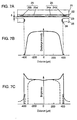
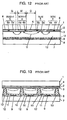
- FIG. 12 is a sectional view taken on line XII-XII of FIG. 9.
- FIG. 13 is a sectional view taken on line XIII-XIII of FIG. 9.
- FIG. 12 and 13 show a dimensional relationship between scan electrode 4 and sustain electrode 5 and a state of a sustain discharge in case of scan electrode SCNi and sustain electrode SUSi in an i line; and scan electrode SCNi+1 and sustain electrode SUSi+1 in an i+1 line.
- a sustain discharge described by a solid line double-headed arrow in FIG. 12 is a discharge between scan electrode SCNi and sustain electrode SUSi in the i the line; or between scan electrode SCNi+1 and sustain electrode SUSi+1 in the i+1 the line, namely scan electrode 4 and sustain electrode 5 in the same line. Therefore, electrode gaps G may be narrow.
- a discharge between sustain electrode SUSi+1 and scan electrode SUSi described by a dotted line double-headed arrow in FIG. 12 is false discharge Y which is undesired sustain discharge. Therefore, the distance D between electrodes of sustain electrode SUSi+1 and scan electrode SCNi is kept wide enough so as for error discharge not to occur.
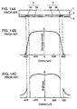
- Scan electrode 4 and sustain electrode 5 comprise transparent electrodes 4a, 5a and bus lines 4b, 5b made of silver and the like respectively. Therefore, bus lines 4b, 5b are opaque. As a result, luminous intensity lowers at the position of bus Lines 4b, 5b as FIG. 14 shows a luminous intensity distribution characteristics. To prevent this lowering of the intensity, reducing electric resistance of bus lines 4b, 5b is kept as low as possible and the bus lines' width is made to be narrow. This prevents a lowering of the intensity resulting from the bus lines' width.
- a distance D between electrodes of sustain electrode SUSi+1 and scan electrode SCNi decreases inevitability as shown in FIG. 15, if the line number M increases to realize high definition. Accordingly, when the line number M increases and exceeds a specific value, a error discharge described by a dotted line double-headed arrow occurs between sustain electrode SUSi and scan electrode SCNi+1. Then the display panel device may not form the display normally.
- bus lines 4b, 5b realizing the high definition makes a ratio of area of bus lines 4b, 5b to an area of transparent electrodes 4a, 5a be increased for bus lines 4b, 5b to get adhesion to transparent electrodes 4a, 5a. As a result, the luminous intensity distribution characteristics lowers at the position of bus lines 4b, 5b
- the present invention provides a high display quality and high definition display panel device which does not have a error discharge and improves luminous intensity, even if a high definition display requires a structure of display electrodes to decrease a distance between the electrodes.
- an AC plasma display device of the present invention comprises:
- This structure allow a distance between a pair of adjacent display electrodes having a non-display portion between the electrodes to be reduced to prevent a error discharge, even if a high definition display requires a structure of display electrodes to decrease a distance between the electrodes.
- FIGs. 1 through 8 An AC plasma display device in accordance with an embodiment of the present invention is described with reference to FIGs. 1 through 8 as follows.
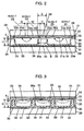
- FIG. 1 is a main perspective view of a panel of an AC plasma display device in accordance with an embodiment of the present invention
- FIG. 2 and FIG. 3 are sectional views taken on lines II-II and III-III of FIG. 1 respectively.
- scan electrode 24 and sustain electrode 25 form a pair referring simply to display electrode 26 in a stripe shape.
- a plurality of the pairs is arranged in parallel on front substrate 21 and covered by dielectric layer 22 and protect film 23 so as to form non-display portion 27 between the pairs.
- Non-display portion 27 is between adjacent display electrodes 26 (pairs of scan electrode 24 and sustain electrode 25) where light shielding layer 28 is located.
- Scan electrode 24 and sustain electrode 25 comprise transparent electrodes 24a and 25a and bus lines 24b and 25b respectively, so as for the bus lines 24b, 25b made of silver and the like to be stick to and electrically connected to the transparent electrodes 24a, 25a, at an end of non-display portion side on the transparent electrodes 24a, 25a respectively.
- transparent electrodes 24a, 25a are of high electric resistance
- forming bus lines 24b, 25b with low resistance material such as silver provide scan electrode 24 and sustain electrode 25 with low resistance.
- an array of data electrodes is placed on rear panel 29 comprising transparent glass substrate and the like.
- the array is covered by insulating layer 30 and in an orthogonal to the display electrodes 26.
- a plurality of partitions 32 made of glass and the like is placed between data electrodes 31on insulating layer 30 in parallel with data electrode 31
- Rear substrate 29 and front substrate 21 are placed facing to each other, so as for data electrodes 31 and display electrodes 26 composed of scan electrodes 24 and sustain electrodes 25 to extend in an orthogonal direction to each other, and to define discharge space 33 between substrates 29 and 21.
- Discharge spaces 33 enclose helium, neon, argon, and xenon or a mixture of some of them as an ionizable gas.
- a discharge cell in the above-described panel structure is formed at a intersection region of data electrode 24 and a display electrode composed of a pair of scan electrode 24 and sustain electrode 25.
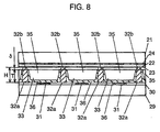
- Belt shaped partitions 32 placed between data electrodes 31 on rear substrate 29 divide discharge space 33 into divided discharge spaces corresponding to data electrodes and define gap dimension H in thickness direction of the panel.
- barrier 35 which is placed at a position facing to non-display portion 27 of front substrate 21 between partitions 32 on rear panel 29, has a width corresponding to non-display portion 27, forms gap 34 between itself and front substrate 27, and prevent error discharges occurring between display electrodes.
- Phosphors 36 emitting red, blue, and green ligthts are arranged in a stripe shape in sequence separated by partition 32 respectively, on the sides of partition 32, the sides of barrier 35, and the surface of insulating layer 28 between partitions 32.
- gap 34 formed by barrier 35 between barrier 35 and front substrate 21 has:
- Above-described panel in accordance with the embodiment of the present invention has barrier 35 preventing error discharge between adjacent display electrodes 26 on rear substrate at a portion facing to non-display portion 27 of front substrate 21. Therefore, even if a high definition display requires display electrode structure having downsized discharge cell, as distinct from a prior art, this structure allow a distance between a pair of adjacent display electrodes 26 having non-display portion 27 between them to be downsized so as to prevent an error discharge
- the embodiment of the present invention has advantages as follows.
- a distance X between bus lines 24b and 25b of adjoining display electrodes 26 sandwiching the non-display portion 27 is narrower than width B in the direction of the length of partition 32. Therefore, opaque bus lines 24b, 25b do not cut off light emission from a dishrag of display electrode 26. As a result, this allows display luminous intensity of a discharge cell to be improved comparing to conventional display panel.
- phosphor 36 is located on sides of barrier 35, phosphor 36 can emits light from the place near to the discharge of display electrode 26. As a result, this allows display brightness of visible light emitted from a discharge cell to be more improved.
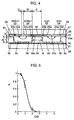
- a display panel in accordance with the example 1 of the present invention is a 42-inch diagonal panel with 480 lines and 852 rows as shown in FIGs. 1, 3, and 4.
- the following conditions are used.
- Electrode gaps G 80 ⁇ m, electrode width W of scan electrode 4 and sustain electrode 5 is 370 ⁇ m, distance D between electrodes is 260 ⁇ m, width B of barrier 35 is 260 ⁇ m, and height H of partition 32 is 120 ⁇ m.
- the figure shows that the probability of error discharge for the panel of the present invention is lower with gap ⁇ decreased namely D/ ⁇ increased, and safely zero when a relation D/ ⁇ 3 is satisfied.
- setting gap ⁇ to lower than 1/3 of distance D between electrodes can prevent the error discharge.
- D/ ⁇ is higher than 3
- the panel is able to have a safety margin for the error discharge to occur.
- barrier 35 allows the probability of occurrence the error discharge to be reduced.
- a 42 inch diagonal panel with specified number of lines and 852 rows with height T of barrier 35 is 80 ⁇ m namely D/ ⁇ 3 .
- An area of distance D between electrodes is investigated about number M of lines, at which an error discharge occurs, with this panel.
- barrier 35 allows the probability of the error discharge to be reduced, even if a high definition display requires display electrodes to decrease a distance between the electrodes.
- a discharge intensity distribution of the panel of the present invention is almost the same as the conventional panel. But, the figures shows that the luminous intensity near scan electrode 24 and bus lines 24b of sustain electrode 24 and 25b of sustain electrode 25 is down to zero in the conventional panel. On the other hand, the intensity at the same portion in the panel of the present invention is higher than intensity at the center of the discharge cell. A measured value of the luminous intensity of the panel of the present invention is about 1.3 times of the luminous intensity of the conventional panel.
- the reason why the above-mentioned intensity is down to zero in the conventional panel is that bus lines 24b, 25b cut off the light emission.
- the reason why the above-mentioned intensity is high in the panel of the present invention, is that bus lines 24b, 25b does not cut off the light emission, and phosphor 36 is located on sides of barrier 35.
- the above-mentioned embodiment of the present invention describes a panel structure for a color display using red, blue, and green phosphors.
- the present invention is adaptable to not only color panel structures, but also panel structures using only one color phosphor, as well as panel structures emitting discharge color light directly without the phosphor.
- a method for driving a panel is not confined to the driving method mentioned above.
- gap 34 is formed by front substrate 21, barrier surface 35 facing to front substrate surface 21a.
- the gap may be replaced by a round hole, a square hole, or a slot formed on the side of barrier 35.
- the method for forming barrier 35 is not only a sandblast method but also a printing method.
- partition 32 with height H is located only on a side of front substrate 21. But, a method for forming gap is not confined to this method. As shown in FIG. 8, partition 32a having the same height as height T of partition 35 and partition 32b with height H - T may be disposed on rear substrate 29 and front substrate 21 respectively.
- the AC plasma display device in accordance with the present invention does not have an error discharge between display electrodes and improves lowering luminous intensity, even if a high definition display requires a structure of display electrodes to decrease a distance between the electrodes. Therefore, the present invention provides a high display quality and high definition display panel device
Landscapes
- Engineering & Computer Science (AREA)
- Physics & Mathematics (AREA)
- Plasma & Fusion (AREA)
- Chemical & Material Sciences (AREA)
- Materials Engineering (AREA)
- Gas-Filled Discharge Tubes (AREA)
Applications Claiming Priority (2)
| Application Number | Priority Date | Filing Date | Title |
|---|---|---|---|
| JP30097299 | 1999-10-22 | ||
| JP30097299 | 1999-10-22 |
Publications (2)
| Publication Number | Publication Date |
|---|---|
| EP1094487A2 true EP1094487A2 (de) | 2001-04-25 |
| EP1094487A3 EP1094487A3 (de) | 2005-10-05 |
Family
ID=17891302
Family Applications (1)
| Application Number | Title | Priority Date | Filing Date |
|---|---|---|---|
| EP00122987A Withdrawn EP1094487A3 (de) | 1999-10-22 | 2000-10-23 | Wechselstrom-Plasmaanzeigevorrichtung |
Country Status (5)
| Country | Link |
|---|---|
| US (1) | US6586879B1 (de) |
| EP (1) | EP1094487A3 (de) |
| KR (1) | KR20010051168A (de) |
| CN (1) | CN1175390C (de) |
| TW (1) | TW498383B (de) |
Cited By (1)
| Publication number | Priority date | Publication date | Assignee | Title |
|---|---|---|---|---|
| EP1939920A4 (de) * | 2006-02-28 | 2009-04-01 | Panasonic Corp | Plasmaanzeigevorrichtung |
Families Citing this family (10)
| Publication number | Priority date | Publication date | Assignee | Title |
|---|---|---|---|---|
| US6680573B1 (en) * | 1999-07-26 | 2004-01-20 | Lg Electronics Inc. | Plasma display panel with improved illuminance |
| JP2003114640A (ja) * | 2001-10-04 | 2003-04-18 | Nec Corp | プラズマディスプレイパネル及びその駆動方法 |
| JP4183421B2 (ja) * | 2002-01-31 | 2008-11-19 | パイオニア株式会社 | プラズマディスプレイパネルの駆動方法及び駆動回路並びに表示装置 |
| EP1361594A3 (de) * | 2002-05-09 | 2005-08-31 | Lg Electronics Inc. | Plasma Anzeigetafel |
| JP2004335280A (ja) * | 2003-05-08 | 2004-11-25 | Pioneer Electronic Corp | プラズマディスプレイパネル |
| US7310073B2 (en) * | 2003-09-01 | 2007-12-18 | Lg Electronics Inc. | Plasma display panel |
| US20090121631A1 (en) * | 2005-08-26 | 2009-05-14 | Masahiro Sawa | Plasma display panel and production method therefor |
| KR20070112550A (ko) * | 2006-05-22 | 2007-11-27 | 엘지전자 주식회사 | 플라즈마 디스플레이 장치 |
| US20080150835A1 (en) * | 2006-12-20 | 2008-06-26 | Lg Electronics Inc. | Plasma display apparatus and driving method thereof |
| CN101663725B (zh) * | 2007-05-07 | 2011-08-24 | 株式会社日立制作所 | 等离子体显示面板 |
Family Cites Families (10)
| Publication number | Priority date | Publication date | Assignee | Title |
|---|---|---|---|---|
| JP3110498B2 (ja) * | 1991-06-28 | 2000-11-20 | 松下電子工業株式会社 | 気体放電型表示装置 |
| EP0554172B1 (de) * | 1992-01-28 | 1998-04-29 | Fujitsu Limited | Plasma Farbanzeige-Vorrichtung von Oberflächenentladungs-Typ |
| US6008582A (en) * | 1997-01-27 | 1999-12-28 | Dai Nippon Printing Co., Ltd. | Plasma display device with auxiliary partition walls, corrugated, tiered and pigmented walls |
| JP3440352B2 (ja) | 1997-05-20 | 2003-08-25 | 大日本印刷株式会社 | プラズマディスプレイパネル |
| JP3705914B2 (ja) * | 1998-01-27 | 2005-10-12 | 三菱電機株式会社 | 面放電型プラズマディスプレイパネル及びその製造方法 |
| JP3116891B2 (ja) | 1998-03-06 | 2000-12-11 | 日本電気株式会社 | プラズマディスプレイパネル |
| KR100304906B1 (ko) * | 1999-02-24 | 2001-09-26 | 구자홍 | 플로팅 전극을 가진 플라즈마 디스플레이 패널 |
| JP3374807B2 (ja) * | 1999-10-19 | 2003-02-10 | 松下電器産業株式会社 | ディスプレイパネル及びその製造方法 |
| TW466537B (en) * | 2000-07-14 | 2001-12-01 | Acer Display Tech Inc | Plasma display panel and the manufacturing method thereof |
| JP3701185B2 (ja) * | 2000-09-06 | 2005-09-28 | 富士通日立プラズマディスプレイ株式会社 | プラズマディスプレイパネルの製造方法 |
-
2000
- 2000-10-18 US US09/690,822 patent/US6586879B1/en not_active Expired - Fee Related
- 2000-10-20 KR KR1020000061903A patent/KR20010051168A/ko not_active Ceased
- 2000-10-20 CN CNB001316583A patent/CN1175390C/zh not_active Expired - Fee Related
- 2000-10-21 TW TW089122187A patent/TW498383B/zh not_active IP Right Cessation
- 2000-10-23 EP EP00122987A patent/EP1094487A3/de not_active Withdrawn
Cited By (1)
| Publication number | Priority date | Publication date | Assignee | Title |
|---|---|---|---|---|
| EP1939920A4 (de) * | 2006-02-28 | 2009-04-01 | Panasonic Corp | Plasmaanzeigevorrichtung |
Also Published As
| Publication number | Publication date |
|---|---|
| EP1094487A3 (de) | 2005-10-05 |
| KR20010051168A (ko) | 2001-06-25 |
| CN1175390C (zh) | 2004-11-10 |
| US6586879B1 (en) | 2003-07-01 |
| CN1295313A (zh) | 2001-05-16 |
| TW498383B (en) | 2002-08-11 |
Similar Documents
| Publication | Publication Date | Title |
|---|---|---|
| US6452333B1 (en) | Plasma display panel | |
| EP0932181B1 (de) | Plasma-Anzeigetafel | |
| US20040113555A1 (en) | Plasma display panel without transparent electrode | |
| US6236160B1 (en) | Plasma display panel with first and second ribs structure | |
| US6586879B1 (en) | AC plasma display device | |
| US20040189199A1 (en) | Plasma display panel | |
| US7196470B2 (en) | Plasma display panel having sustain electrode arrangement | |
| KR20010030149A (ko) | 플라즈마표시패널의 장치, 제조방법 및 구동방법 | |
| US6437514B1 (en) | AC plasma display device | |
| US20050122045A1 (en) | Plasma display panel | |
| KR100647618B1 (ko) | 플라즈마 디스플레이 패널 | |
| US7576495B2 (en) | Plasma display panel | |
| US7652427B2 (en) | Plasma display panel | |
| KR100778419B1 (ko) | 플라즈마 디스플레이 패널 | |
| US20060145613A1 (en) | Plasma display apparatus | |
| KR20000009188A (ko) | 플라즈마 디스플레이 패널 | |
| US7629747B2 (en) | Plasma display panel having specific electrode structure | |
| KR100599679B1 (ko) | 플라즈마 디스플레이 패널 | |
| KR100592297B1 (ko) | 플라즈마 디스플레이 패널 | |
| KR100669697B1 (ko) | 전극 구조가 개선된 플라즈마 디스플레이 패널 | |
| US20060012302A1 (en) | Plasma display panel | |
| KR100599680B1 (ko) | 플라즈마 디스플레이 패널 | |
| KR100536195B1 (ko) | 플라즈마 디스플레이 패널 | |
| KR100669329B1 (ko) | 플라즈마 디스플레이 패널 | |
| US8304992B2 (en) | Plasma display panel including a black layer |
Legal Events
| Date | Code | Title | Description |
|---|---|---|---|
| PUAI | Public reference made under article 153(3) epc to a published international application that has entered the european phase |
Free format text: ORIGINAL CODE: 0009012 |
|
| AK | Designated contracting states |
Kind code of ref document: A2 Designated state(s): AT BE CH CY DE DK ES FI FR GB GR IE IT LI LU MC NL PT SE |
|
| AX | Request for extension of the european patent |
Free format text: AL;LT;LV;MK;RO;SI |
|
| PUAL | Search report despatched |
Free format text: ORIGINAL CODE: 0009013 |
|
| AK | Designated contracting states |
Kind code of ref document: A3 Designated state(s): AT BE CH CY DE DK ES FI FR GB GR IE IT LI LU MC NL PT SE |
|
| AX | Request for extension of the european patent |
Extension state: AL LT LV MK RO SI |
|
| 17P | Request for examination filed |
Effective date: 20051223 |
|
| AKX | Designation fees paid |
Designated state(s): AT BE CH CY DE DK ES FI FR GB GR IE IT LI LU MC NL PT SE |
|
| 17Q | First examination report despatched |
Effective date: 20071008 |
|
| RAP1 | Party data changed (applicant data changed or rights of an application transferred) |
Owner name: PANASONIC CORPORATION |
|
| GRAP | Despatch of communication of intention to grant a patent |
Free format text: ORIGINAL CODE: EPIDOSNIGR1 |
|
| RIC1 | Information provided on ipc code assigned before grant |
Ipc: H01J 17/49 20120101AFI20130404BHEP Ipc: H01J 11/12 20120101ALI20130404BHEP Ipc: H01J 11/24 20120101ALI20130404BHEP Ipc: H01J 11/36 20120101ALI20130404BHEP Ipc: H01J 11/32 20120101ALI20130404BHEP |
|
| INTG | Intention to grant announced |
Effective date: 20130429 |
|
| STAA | Information on the status of an ep patent application or granted ep patent |
Free format text: STATUS: THE APPLICATION IS DEEMED TO BE WITHDRAWN |
|
| 18D | Application deemed to be withdrawn |
Effective date: 20130910 |