EP1094328A1 - Magnetfeldsensor mit Kettenleiterfilter - Google Patents
Magnetfeldsensor mit Kettenleiterfilter Download PDFInfo
- Publication number
- EP1094328A1 EP1094328A1 EP00122905A EP00122905A EP1094328A1 EP 1094328 A1 EP1094328 A1 EP 1094328A1 EP 00122905 A EP00122905 A EP 00122905A EP 00122905 A EP00122905 A EP 00122905A EP 1094328 A1 EP1094328 A1 EP 1094328A1
- Authority
- EP
- European Patent Office
- Prior art keywords
- ota
- filter
- signal
- magnetic field
- capacitor
- Prior art date
- Legal status (The legal status is an assumption and is not a legal conclusion. Google has not performed a legal analysis and makes no representation as to the accuracy of the status listed.)
- Granted
Links
- 230000000306 recurrent effect Effects 0.000 title 1
- 239000003990 capacitor Substances 0.000 claims abstract description 40
- 239000004020 conductor Substances 0.000 claims description 8
- 238000005516 engineering process Methods 0.000 claims description 4
- 238000010276 construction Methods 0.000 claims description 2
- 238000010586 diagram Methods 0.000 description 4
- 230000003321 amplification Effects 0.000 description 3
- 230000001419 dependent effect Effects 0.000 description 3
- 230000001939 inductive effect Effects 0.000 description 3
- 238000003199 nucleic acid amplification method Methods 0.000 description 3
- 230000002123 temporal effect Effects 0.000 description 3
- 238000001514 detection method Methods 0.000 description 2
- 230000000694 effects Effects 0.000 description 2
- 238000005259 measurement Methods 0.000 description 2
- 238000012935 Averaging Methods 0.000 description 1
- 230000009286 beneficial effect Effects 0.000 description 1
- 238000011161 development Methods 0.000 description 1
- 230000018109 developmental process Effects 0.000 description 1
- 230000009977 dual effect Effects 0.000 description 1
- 238000000034 method Methods 0.000 description 1
- 230000000717 retained effect Effects 0.000 description 1
- 238000009751 slip forming Methods 0.000 description 1
- 230000001629 suppression Effects 0.000 description 1
- 230000009466 transformation Effects 0.000 description 1
Images


Classifications
-
- G—PHYSICS
- G01—MEASURING; TESTING
- G01R—MEASURING ELECTRIC VARIABLES; MEASURING MAGNETIC VARIABLES
- G01R33/00—Arrangements or instruments for measuring magnetic variables
- G01R33/02—Measuring direction or magnitude of magnetic fields or magnetic flux
- G01R33/06—Measuring direction or magnitude of magnetic fields or magnetic flux using galvano-magnetic devices
- G01R33/07—Hall effect devices
-
- H—ELECTRICITY
- H03—ELECTRONIC CIRCUITRY
- H03F—AMPLIFIERS
- H03F2200/00—Indexing scheme relating to amplifiers
- H03F2200/261—Amplifier which being suitable for instrumentation applications
Definitions
- the invention relates to a magnetic field sensor with a Hall element and with a Orthogonal switch that connects between connections for the supply current for the Hall element and connections for the Hall voltage depending on one Clock signal switches back and forth, and with a filter circuit that the orthogonal switch filter delivered signal.
- Such a magnetic field sensor is from DE-A-44 31 703 by the same applicant known. Due to the orthogonal switchover, the one occurring at the Hall element Offset voltage largely eliminated on average over time, whereby the Overall measurement accuracy is increased.
- a disadvantage of the known magnetic field sensor is that as a result of the orthogonal switchover the output signal over the Time is not exactly constant, but results at the switching times is a discontinuous course because the offset voltage is the Hall voltage superimposed in a rectangular shape and the operating state for a short time at the changeover times is not defined due to switching differences that are always present. The output signal is therefore subject to errors at least at these switching times and cannot be evaluated.
- the invention uses a chain ladder filter as the filter circuit, in which each Stage contained capacitor in the first clock phase with the if necessary amplified difference signal and in the second clock phase with the inverted Differential signal is applied.
- This is due to the orthogonal switch useful signal contained in the difference signal, which corresponds to the detected magnetic field, also inverse to each other in the two clock phases. Be accordingly those in the differential signal based on the electronic components per filter stage overlapping common mode signals, e.g. Offset voltages, on average over time balanced. Such common mode signals that occur thus become total eliminated, while the useful signal supplied by the orthogonal switch with high Accuracy is reproduced if necessary.
- Using the chain ladder filter low-pass filters with a low cut-off frequency can be implemented. Hence can be generated by the magnetic field sensor and as a result of chopper operation discontinuous signal continuously delivered over time and processed further.
- An embodiment of the invention uses an active filter circuit Chain ladder filter.
- a chain ladder filter is described, for example, in IEEE J. Solid-State Circuits, vol. SC-26, no. 12, pp. 1988 - 1997, Dec. 1991.
- a Such chain ladder filter has the advantage that it has excellent filter characteristics has and can be manufactured relatively easily in CMOS technology.
- Amplifier elements are preferably OTA (operational transconductance amplifier) that work in gyrator circuit. These OTA building blocks are also known as transconductance amplifiers.
- the gyrator circuit enables the transformation of an impedance into the dual impedance.
- inductive components can be one Implement filters using capacitors. That is how it is Small chain ladder filter can be implemented as a monolithic circuit, although it contains to a significant extent inductive components that are considered passive LC ladder filter would require a significant amount of space to to generate the desired filter behavior, but not monolithic would be.
- OTA modules have a significant offset component, which means that the output signal of the active ladder filter overall is considerable Includes offset voltage. Such an offset voltage would be due to the orthogonal Switching achievable measurement accuracy of the detection of the magnetic field destroy again.
- OTA modules are connected in series in the chain ladder filter with their inputs and outputs in one Chopper mode switched so that the resulting offset voltages, which show up as voltages across the capacitors in successive Compensate clock phases.
- the output voltages of the OTA modules are alternately fed to the capacitors depending on the clock signal, i.e. in a first clock phase via the inverting output to the first Capacitor and in a second clock phase over the same inverting Output the second capacitor.
- FIG. 1 is a circuit arrangement for a magnetic field sensor according to the invention shown as a block diagram.
- a Hall element 1 has a first pair of terminals 2, 2 and a second pair of terminals 3, 3. Terminals 2, 2 and 3, 3 are connected to an orthogonal switch 4, which has a clock signal T is controlled.
- the orthogonal switch 4 is also with a power supply unit 5 connected, the control current for the Hall element 1 provides.
- the voltage U1 tapped.
- the orthogonal switch 4 is programmed so that it depending on the clock signal T in a first clock phase P1 via the terminals 2, 2 a current I1 from the voltage supply unit 5 to the Hall element 1 feeds. In this phase P1, the Hall voltage can be connected to terminals 3, 3 U1 can be tapped.
- the amount is the same Control current I2 supplied to terminals 3, 3; the Hall voltage then turns on tapped at terminals 2, 2, i.e. the voltage U1 corresponds to the voltage terminals 2, 2.
- the voltage U1 in addition to a useful signal component, which is proportional to the magnetic field to which the Hall element 1 is exposed contain the offset voltage of the Hall element 1, which is due to a non-ideal Geometry of the Hall element and due to piezoresistive effects during pressing of the Hall element in the plastic housing.
- the useful signal components remain aligned in both clock phases P1 and P2; against that they stand out Offset signal components in the voltage U1 in successive phases P1, P2 on and can be eliminated. A more detailed description this effect is described in DE-A-44 31 703 by the same applicant. This document is hereby incorporated by reference into the disclosure of the present Registration added.
- FIG. 2 shows schematically as an embodiment of a circuit arrangement for an active chain ladder filter that is implemented in CMOS technology.
- the chain ladder filter is of the type of a Gm-C filter, which often corresponds to the Anglo-Saxon Also called a transconductance-capacitor-continuous-time filter is designated.
- the structure of such a filter and the filter behavior is described in more detail in IEEE J. Solid-State Circuits, vol. SC-26, no. 12, pp. 1988 - 1997, Dec. 1991.
- the ladder filter according to the invention contains six OTA blocks gm0, gm1, gm2, gm3, gm4, gm5.
- the OTA modules work in Gyrator circuit, i.e. they generate an inductive behavior using of capacitors.
- a low-pass filter with a low cutoff frequency and high quality can be realized without the need for real inductors become.
- Other active chain ladder filters for example an RC chain ladder filter correspond or operational amplifiers instead of transconductance amplifiers included, can also be used with suitable dimensions.
- Each OTA module gm0 to gm5 has two inverting inputs, one with Minus signs are labeled. Furthermore, each OTA block has two non-inverting ones Entrances marked with a plus sign. The inverting Outputs of the OTA blocks are marked with a minus sign and the non-inverting ones Exits marked with a plus sign.
- the OTA building block gm0 is designed as an input amplifier; the other OTA modules gm1 to gm5 are with their outputs against capacitors C1, C2 over Switch S switched. In the embodiment of Figure 2 and Figure 3 are the simpler description and illustration because of all capacitors C1, C2 chosen the same size. The switches S are dependent on their switching positions switched by the clock signal T.
- the switches S In the first clock phase P1, the switches S have the Positions shown in Figure 2. In the second clock phase P2, the Switch S, so that the other outputs on the capacitors C1, C2 with the opposite polarity of the relevant OTA module.
- the Output voltage U2 of the chain ladder filter is at the one on the right in FIG Capacitors C1, C2 tapped as differential voltage. opposite the embodiment of Figure 2 and Figure 3 with two capacitors C1, C2 it is also possible for each OTA module, only one for each OTA module To use capacitor Cg, which is then ground-free between the inverting and non-inverting output is connected.
- FIG. 3 shows an example of the wiring for the OTA building blocks gm3 and gm4.
- the OTA blocks have gm3 and gm4 a first non-inverting input 14a, 14b and a second non-inverting Input 16a, 16b, a first inverting input 18a, 18b and a second inverting input 20a, 20b.
- the OTA modules have gm3, gm4 an inverting output 22a, 22b and a non-inverting Output 24a, 24b.
- the inverting outputs 22a, 22b are over Switch S connected to a capacitor C1; as are the non-inverting ones Outputs 24a and 24b are connected to capacitors C2 via switches S.
- the differential voltage signal of the previous OTA module gm2 is that OTA module gm3 at its first non-inverting input 14a and on fed to its first inverting input 18a.
- the inverting output 22b of the downstream OTA module gm4 is inverting with the second Input 20a of the OTA module gm3 connected.
- the non-inverting output 24b of the OTA module gm4 is with the second non-inverting input 16a of the OTA module gm3 connected.
- the switch position of the switches S is dependent on the clock signal T. controlled.
- the position shown in FIG. 3 applies to the first clock phase P1.
- the first clock phase P1 are the inverting outputs 22a, 22b of the first OTA module gm3 and the second OTA module gm4 each with the first capacitor C1 connected.
- the non-inverting outputs 24a, 24b of the first OTA module gm3 and the second OTA module gm4 are connected to the second capacitor C2.
- the Capacitors C1, C2 are charged in accordance with the circuitry mentioned.
- the switches S are switched to their other position, which is shown in dashed lines in FIG.
- the capacitors C1, C2 then become the switches according to this switch position S loaded.
- switches S depending on the clock signal a chopper operation is implemented.
- this chopper operation signal outputs for charging the capacitors C1, C2 constantly interchanged.
- the offset signals occurring at the OTA modules are replaced by a Averaging suppressed over time. Since the clock signal T simultaneously both the switch S and the orthogonal switch 4 controls remain in the case of the downstream chain conductor filter, the offset voltage suppression as a result the orthogonal switchover.
- the dimensioning of the transconductances gm of the individual OTA modules Determine gm0 to gm5 and the size of the integrated capacitors C1, C2, Cg the frequency response of the ladder filter.
- the dimensioning of the elements the chain ladder filter is preferably designed so that all capacities as different multiples of a basic capacitance C0 and all transconductances chosen as different multiples of a basic transconductance gm0 become.
- the quotient gm0 / C0 determines the cutoff frequency of the filter while the amplification by the relationships of the transconductances to each other is determined.
- the transconductance level is set in that the respective OTA module gm1 to gm5 that of the main signal flow direction (corresponds to the inputs in FIG. 3) 14a, 14b or 18a, 18b) associated transconductance is greater than that of the signal feedback direction (corresponds to the inputs 16a, 20a and 16b in FIG. 3, 20b) is assigned transconductance.
- the ratio of these transconductances gm for example 3: 1 then the associated OTA component has the signal amplification factor 3. If both transconductances gm are the same, then the signal amplification factor 1 and the signal is not changed in size.
- the chain ladder filter has a low-pass function.
- the filter frequency of this low pass is at least a factor of 2 smaller than the frequency of the clock signal T, which of the chopper frequency, e.g. Corresponds to 300 kHz.
- This filter frequency is in the exemplary embodiment by a factor of 5 less than the frequency of the clock signal T.
- the cutoff frequency of the ladder filter is in the range from 30 kHz to 100 kHz, preferably in the range of 60 kHz. With this dimensioning is for a Hall signal, the useful signal frequency range of 0 Hz up to approx. 10 kHz, a continuous output signal with a high temporal Resolution is created without discontinuities.
- the voltage U1 at the input of the chain ladder filter alternates the sum and difference of the offset voltage of the Hall element 1 and Hall voltage on.
- the Hall voltage is continuously formed in the correct phase, i.e. the Voltages on the capacitors C1, C2 correspond to the respective Hall voltage, which is a low frequency continuous signal or even a DC signal is.
- the offset voltages appear in phase on the capacitors C1, C2 as alternating signals and are due to the low-pass filter characteristic of Filtered chain ladder filter. Accordingly, at the outlet of the chain ladder filter generates the offset-free, low-pass filtered voltage U2, that of the Hall element 1 emitted Hall voltage corresponds to the size of the magnetic field.
- the Hall voltage can the chain conductor filter in Useful signal frequency range, for example in the range from 0 Hz to 10 kHz, undamped happen while the offset voltage of Hall element 1 and the Offset voltages of the OTA modules gm0 to gm5 as alternating signals on the Chopper frequency, for example 300 kHz, can be modulated.
- the ladder filter for example with a low-pass filter frequency of 60 kHz, this alternating signal is filtered out.
- a voltage U2 forms at the output of the chain ladder filter, in which the occurring offset voltages are suppressed.
- the filter can be inexpensive in CMOS technology as a transconductance C filter, i.e. designed as a Gm-C filter become.
- the entire magnetic field sensor can thus be in a small size a component together with the chain ladder filter as a monolithic integrable Circuit can be realized.
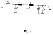
- FIG. 4 shows an LCR equivalent circuit diagram of the chain ladder filter shown in FIG. 2.
- the inductors L are realized by the gyrator circuit of the OTA modules.
- Resistors R1 and R2 are set by parameter settings OTA blocks gm0 to gm5 defined.
- the equivalent circuit diagram defines a multi-stage low-pass filter.
Landscapes
- Physics & Mathematics (AREA)
- Condensed Matter Physics & Semiconductors (AREA)
- General Physics & Mathematics (AREA)
- Measuring Magnetic Variables (AREA)
Abstract
Description
- Figur 1
- eine Schaltungsanordnung für ein Hallelement mit einem Orthogonalumschalter,
- Figur 2
- den Aufbau eines Kettenleiterfilters nach Art eines Gm-C-Filters,
- Figur 3
- zwei hintereinander geschaltete OTA-Bausteine des Kettenleiterfilters und deren Beschaltung,
- Figur 4
- ein Ersatzschaltbild mit R-, L-, C-Elementen für den Kettenleiterfilter.
Claims (9)
- Magnetfeldsensor mit einem Hallelement (1) und mit einem Orthogonalumschalter (4), der zwischen Anschlüssen für den Versorgungsstrom für das Hallelement (1) und Anschlüssen für die Hallspannung abhängig von einem Taktsignal (T) hin- und herschaltet,und mit einer Filterschaltung, die das vom Orthogonalumschalter (4) gelieferte Signal (U1) filtert,
dadurch gekennzeichnet, daß als Filterschaltung ein mehrstufiges Kettenleiterfilter vorgesehen ist, dem das Signal (u1) als Differenzsignal zugeführt ist,und daß jede Stufe mindestens einen Kondensator (C1, Cg) enthält, der abhängig vom Taktsignal (T) in einer ersten Taktphase (P1) mit dem gegebenenfalls verstärkten Differenzsignal und in einer zweiten Taktphase (P2) mit dem invertierten Differenzsignal beaufschlagt ist. - Magnetfeldsensor nach Anspruch 1, dadurch gekennzeichnet, daß das Kettenleiterfilter als aktives Kettenleiterfilter ausgebildet ist, der vorzugsweise OTA-Bausteine enthält.
- Magnetfeldsensor nach Anspruch 2, dadurch gekennzeichnet, daß das aktive Kettenleiterfilter mindestens zwei hintereinander geschaltete OTA-Bausteine (gm3, gm4) enthält, die in Gyratorschaltung arbeiten,daß jeder OTA-Baustein (gm3, gm4) einen ersten nicht-invertierenden Eingang (14a, 14b) und einen zweiten nicht-invertierenden Eingang (16a, 16b), einen ersten invertierenden Eingang (18a, 18b) und einen zweiten invertierenden Eingang (20a, 20b), sowie einen invertierenden Ausgang (22a, 22b) und einen nicht-invertierenden Ausgang (24a, 24b) hat,daß das gegebenenfalls verstärkte Signal (U1) dem ersten OTA-Baustein (gm3) am ersten nicht-invertierenden Eingang (14a) und am ersten invertierenden Eingang (18a) zugeführt ist,daß den OTA-Bausteinen (gm3, gm4) jeweils ein erster Kondensator (C1) und ein zweiter Kondensator (C2) oder ein gemeinsamer Kondensator (Cg) zugeordnet ist,daß der invertierende Ausgang (22b) des dem ersten OTA-Baustein (gm3) nachgeschalteten zweiten OTA-Bausteins (gm4) mit dem zweiten invertierenden Eingang (20a) des ersten OTA-Bausteins (gm3) verbunden ist,daß der nicht-invertierende Ausgang (24b) des zweiten OTA-Bausteins (gm4) mit dem zweiten nicht-invertierenden Eingang (16a) des ersten OTA-Bausteins (gm3) verbunden ist,daß abhängig vom Taktsignal (T) in der ersten Taktphase (P1) die invertierenden Ausgänge (22a, 22b) des ersten OTA-Bausteins (gm3) und des zweiten OTA-Bausteins (gm4) jeweils mit dem ersten Kondensator (C1) oder mit dem ersten Anschluß des gemeinsamen Kondensators (Cg) und die nicht-invertierenden Ausgänge (24a, 24b) des ersten OTA-Bausteins (gm3) und des zweiten OTA-Bausteins (gm4) jeweils mit dem zweiten Kondensator (C2) oder mit dem zweiten Anschluß des gemeinsamen Kondensators (Cg) verbunden sind,und daß in der zweiten Taktphase (P2) des Taktsignals (T) die invertierenden Ausgänge (22a, 22b) des ersten OTA-Bausteins (gm3) und des zweiten OTA-Bausteins (gm4) jeweils mit dem zweiten Kondensator (C2) oder mit dem zweiten Anschluß des gemeinsamen Kondensators (Cg) und die nicht-invertierenden Ausgänge (24a, 24b) des ersten OTA-Bausteins (gm3) und des zweiten OTA-Bausteins (gm4) mit dem ersten Kondensator (C1) mit dem ersten Anschluß des gemeinsamen Kondensators (Cg) zur Realisierung eines Chopper-Betriebs miteinander verbunden sind.
- Magnetfeldsensor nach Anspruch 3, gekennzeichnet durch weitere OTA-Bausteine (gm1, gm2, gm5) mit einer Beschaltung nach Art des ersten und zweiten OTA-Bausteins (gm3, gm4) zum Aufbau eines mehrstufigen Kettenleiterfilters.
- Magnetfeldsensor nach einem der vorhergehenden Ansprüche, dadurch gekennzeichnet, daß das Kettenleiterfilter als Tiefpaßfilter mit einer Filterfrequenz mindestens um den Faktor 2 kleiner als die Frequenz des Taktsignals (T) geschaltet ist, vorzugsweise um den Faktor 5 kleiner.
- Magnetfeldsensor nach Anspruch 5, dadurch gekennzeichnet, daß die Grenzfrequenz des Kettenleiterfilters im Bereich von 30 kHz bis 100 kHz, vorzugsweise im Bereich von 60 kHz liegt.
- Magnetfeldsensor nach einem der vorhergehenden Ansprüche, dadurch gekennzeichnet, daß das Kettenleiterfilter in CMOS-Technologie als Transconductance-C-Filter realisiert ist.
- Magnetfeldsensor nach einem der vorhergehenden Ansprüche, dadurch gekennzeichnet, daß zur Realisierung des Chopper-Betriebs die Kondensatoren (C1, C2) mittels CMOS-Schalter mit den Ausgängen (22a, 22b; 24a, 24b) der OTA-Bausteine (gm3, gm4) verbunden sind.
- Magnetfeldsensor nach einem der vorhergehenden Ansprüche, dadurch gekennzeichnet, daß mindestens bei einem OTA-Baustein (gm1 bis gm5) die der Signalhauptflußrichtung zugeordnete Transkonduktanz größer als die der Signalrückführungsrichtung zugeordnete Transkonduktanz ist.
Applications Claiming Priority (2)
| Application Number | Priority Date | Filing Date | Title |
|---|---|---|---|
| DE19951045 | 1999-10-22 | ||
| DE19951045A DE19951045B4 (de) | 1999-10-22 | 1999-10-22 | Magnetfeldsensor mit Kettenleiterfilter |
Publications (2)
| Publication Number | Publication Date |
|---|---|
| EP1094328A1 true EP1094328A1 (de) | 2001-04-25 |
| EP1094328B1 EP1094328B1 (de) | 2005-07-27 |
Family
ID=7926606
Family Applications (1)
| Application Number | Title | Priority Date | Filing Date |
|---|---|---|---|
| EP00122905A Expired - Lifetime EP1094328B1 (de) | 1999-10-22 | 2000-10-20 | Magnetfeldsensor mit Kettenleiterfilter |
Country Status (3)
| Country | Link |
|---|---|
| US (1) | US6433544B1 (de) |
| EP (1) | EP1094328B1 (de) |
| DE (2) | DE19951045B4 (de) |
Families Citing this family (4)
| Publication number | Priority date | Publication date | Assignee | Title |
|---|---|---|---|---|
| DE19943128A1 (de) * | 1999-09-09 | 2001-04-12 | Fraunhofer Ges Forschung | Hall-Sensoranordnung zur Offset-kompensierten Magnetfeldmessung |
| JP5385490B1 (ja) | 2012-01-25 | 2014-01-08 | 旭化成エレクトロニクス株式会社 | ホール起電力信号検出回路及びその電流センサ |
| IT201700071213A1 (it) * | 2017-06-26 | 2018-12-26 | St Microelectronics Srl | Circuito di lettura per sensori hall, dispositivo e procedimento corrispondenti |
| CN108106642B (zh) * | 2017-12-20 | 2019-12-27 | 苏州闻颂智能科技有限公司 | 一种霍尔元件模拟前端电路 |
Citations (4)
| Publication number | Priority date | Publication date | Assignee | Title |
|---|---|---|---|---|
| DE4431703A1 (de) * | 1994-09-06 | 1996-03-28 | Itt Ind Gmbh Deutsche | Magnetfeldsensor mit Hallelement |
| US5621319A (en) * | 1995-12-08 | 1997-04-15 | Allegro Microsystems, Inc. | Chopped hall sensor with synchronously chopped sample-and-hold circuit |
| EP0793075A1 (de) * | 1996-03-02 | 1997-09-03 | Deutsche ITT Industries GmbH | Monolithisch integrierte Sensorschaltung |
| WO1999021023A1 (en) * | 1997-10-20 | 1999-04-29 | Analog Devices, Inc. | Monolithic magnetic sensor having externally adjustable temperature compensation |
Family Cites Families (2)
| Publication number | Priority date | Publication date | Assignee | Title |
|---|---|---|---|---|
| DE19543562A1 (de) * | 1994-11-22 | 1996-05-23 | Bosch Gmbh Robert | Anordnung zur berührungslosen Drehwinkelerfassung eines drehbaren Elements |
| ATE345510T1 (de) * | 1996-09-09 | 2006-12-15 | Ams Internat Ag | Verfahren zum reduzieren der offsetpannung einer hallanordnung |
-
1999
- 1999-10-22 DE DE19951045A patent/DE19951045B4/de not_active Expired - Fee Related
-
2000
- 2000-10-20 EP EP00122905A patent/EP1094328B1/de not_active Expired - Lifetime
- 2000-10-20 US US09/693,537 patent/US6433544B1/en not_active Expired - Fee Related
- 2000-10-20 DE DE50010819T patent/DE50010819D1/de not_active Expired - Lifetime
Patent Citations (4)
| Publication number | Priority date | Publication date | Assignee | Title |
|---|---|---|---|---|
| DE4431703A1 (de) * | 1994-09-06 | 1996-03-28 | Itt Ind Gmbh Deutsche | Magnetfeldsensor mit Hallelement |
| US5621319A (en) * | 1995-12-08 | 1997-04-15 | Allegro Microsystems, Inc. | Chopped hall sensor with synchronously chopped sample-and-hold circuit |
| EP0793075A1 (de) * | 1996-03-02 | 1997-09-03 | Deutsche ITT Industries GmbH | Monolithisch integrierte Sensorschaltung |
| WO1999021023A1 (en) * | 1997-10-20 | 1999-04-29 | Analog Devices, Inc. | Monolithic magnetic sensor having externally adjustable temperature compensation |
Non-Patent Citations (1)
| Title |
|---|
| KHOURY J M: "DESIGN OF A 15-MHZ CMOS CONTINUOUS-TIME FILTER WITH ON-CHIP TUNING", IEEE JOURNAL OF SOLID-STATE CIRCUITS,US,IEEE INC. NEW YORK, vol. 26, no. 12, 1 December 1991 (1991-12-01), pages 1988 - 1997, XP000272860, ISSN: 0018-9200 * |
Also Published As
| Publication number | Publication date |
|---|---|
| US6433544B1 (en) | 2002-08-13 |
| DE50010819D1 (de) | 2005-09-01 |
| DE19951045B4 (de) | 2005-03-17 |
| DE19951045A1 (de) | 2001-05-31 |
| EP1094328B1 (de) | 2005-07-27 |
Similar Documents
| Publication | Publication Date | Title |
|---|---|---|
| EP0793075B1 (de) | Monolithisch integrierte Sensorschaltung | |
| DE69431721T2 (de) | Elektrische ladungsübertragungsanordnung | |
| DE2825882C2 (de) | Schaltungsanordnung zur Reduzierung niederfrequenter Störspannung und Offsetspannung bei einer Verstärkerschaltung | |
| EP0418753B1 (de) | Offsetspannungsabgleichender Operationsverstärker | |
| DE3422716C2 (de) | ||
| DE10204427A1 (de) | Verfahren und Vorrichtung zur Kompensation dynamischer Fehlersignale eines Chopped-Hall-Sensors | |
| DE102004052174B4 (de) | Verstärkerschaltung, umfassend einen Verstärker mit tiefpassgefilterter Rückkopplung | |
| EP0039076A1 (de) | Integratorschaltung mit Abtaststufe | |
| DE2815671A1 (de) | Abstimmbares bandpassfilter und signalprozessor, welcher das abstimmbare bandpassfilter enthaelt | |
| DE3309897C2 (de) | ||
| EP1310043A1 (de) | Differentieller, komplementärer verstärker | |
| EP1094328B1 (de) | Magnetfeldsensor mit Kettenleiterfilter | |
| DE3513167A1 (de) | Ansteuerungsschaltung fuer kollektorlose gleichstrommotoren | |
| DE3603841C2 (de) | Dämpfungsglied mit niedrigem Rauschverhalten und hoher thermischer Stabilität | |
| DE3818142A1 (de) | Verstaerkerschaltung mit einem einzigen kondensator fuer gleichspannungsabgleich | |
| EP0133618A1 (de) | Monolithisch integrierte Transistor-Hochfreqzenz-Quarzoszillatorschaltung | |
| WO2003049282A1 (de) | Voll differentieller differenzverstärker mit hoher eingangsimpedanz | |
| DE3109375C2 (de) | ||
| DE102019219759B4 (de) | Schaltungsanordnung zum Erfassen eines durch eine bipolare Last fließenden Stroms | |
| DE3816140A1 (de) | Videosignalumschalter | |
| DE3525201A1 (de) | Aktive tiefpassfilterschaltung | |
| DE2213712A1 (de) | Matrix Schaltungsanordnung | |
| EP0149023A1 (de) | Endstufenanordnung | |
| EP0236538B1 (de) | Schaltungsanordnung mit einem am Eingang einpolig angeschlossenen Vierpol und einem Verstärker zur Kompensation eines Bezugspotentials | |
| DE102004057094B4 (de) | Kapazitives Element |
Legal Events
| Date | Code | Title | Description |
|---|---|---|---|
| PUAI | Public reference made under article 153(3) epc to a published international application that has entered the european phase |
Free format text: ORIGINAL CODE: 0009012 |
|
| 17P | Request for examination filed |
Effective date: 20010301 |
|
| AK | Designated contracting states |
Kind code of ref document: A1 Designated state(s): BE DE FR GB IT Kind code of ref document: A1 Designated state(s): BE DE FR GB IT NL |
|
| AX | Request for extension of the european patent |
Free format text: AL;LT;LV;MK;RO;SI |
|
| AKX | Designation fees paid |
Free format text: BE DE FR GB IT NL |
|
| RBV | Designated contracting states (corrected) |
Designated state(s): BE DE FR GB IT |
|
| 17Q | First examination report despatched |
Effective date: 20030617 |
|
| GRAP | Despatch of communication of intention to grant a patent |
Free format text: ORIGINAL CODE: EPIDOSNIGR1 |
|
| RBV | Designated contracting states (corrected) |
Designated state(s): BE DE FR GB IT NL |
|
| GRAS | Grant fee paid |
Free format text: ORIGINAL CODE: EPIDOSNIGR3 |
|
| GRAA | (expected) grant |
Free format text: ORIGINAL CODE: 0009210 |
|
| AK | Designated contracting states |
Kind code of ref document: B1 Designated state(s): BE DE FR GB IT NL |
|
| REG | Reference to a national code |
Ref country code: GB Ref legal event code: FG4D Free format text: NOT ENGLISH |
|
| REF | Corresponds to: |
Ref document number: 50010819 Country of ref document: DE Date of ref document: 20050901 Kind code of ref document: P |
|
| GBT | Gb: translation of ep patent filed (gb section 77(6)(a)/1977) |
Effective date: 20051003 |
|
| ET | Fr: translation filed | ||
| PLBE | No opposition filed within time limit |
Free format text: ORIGINAL CODE: 0009261 |
|
| STAA | Information on the status of an ep patent application or granted ep patent |
Free format text: STATUS: NO OPPOSITION FILED WITHIN TIME LIMIT |
|
| 26N | No opposition filed |
Effective date: 20060428 |
|
| PGFP | Annual fee paid to national office [announced via postgrant information from national office to epo] |
Ref country code: NL Payment date: 20091016 Year of fee payment: 10 |
|
| PGFP | Annual fee paid to national office [announced via postgrant information from national office to epo] |
Ref country code: IT Payment date: 20091023 Year of fee payment: 10 |
|
| REG | Reference to a national code |
Ref country code: NL Ref legal event code: V1 Effective date: 20110501 |
|
| PG25 | Lapsed in a contracting state [announced via postgrant information from national office to epo] |
Ref country code: NL Free format text: LAPSE BECAUSE OF NON-PAYMENT OF DUE FEES Effective date: 20110501 |
|
| PG25 | Lapsed in a contracting state [announced via postgrant information from national office to epo] |
Ref country code: IT Free format text: LAPSE BECAUSE OF NON-PAYMENT OF DUE FEES Effective date: 20101020 |
|
| PGFP | Annual fee paid to national office [announced via postgrant information from national office to epo] |
Ref country code: GB Payment date: 20131021 Year of fee payment: 14 Ref country code: FR Payment date: 20131022 Year of fee payment: 14 Ref country code: BE Payment date: 20131022 Year of fee payment: 14 Ref country code: DE Payment date: 20131021 Year of fee payment: 14 |
|
| REG | Reference to a national code |
Ref country code: DE Ref legal event code: R119 Ref document number: 50010819 Country of ref document: DE |
|
| REG | Reference to a national code |
Ref country code: DE Ref legal event code: R082 Ref document number: 50010819 Country of ref document: DE Representative=s name: SCHAUMBURG & PARTNER PATENTANWAELTE GBR, DE |
|
| GBPC | Gb: european patent ceased through non-payment of renewal fee |
Effective date: 20141020 |
|
| PG25 | Lapsed in a contracting state [announced via postgrant information from national office to epo] |
Ref country code: BE Free format text: LAPSE BECAUSE OF NON-PAYMENT OF DUE FEES Effective date: 20141031 |
|
| PG25 | Lapsed in a contracting state [announced via postgrant information from national office to epo] |
Ref country code: GB Free format text: LAPSE BECAUSE OF NON-PAYMENT OF DUE FEES Effective date: 20141020 Ref country code: DE Free format text: LAPSE BECAUSE OF NON-PAYMENT OF DUE FEES Effective date: 20150501 |
|
| REG | Reference to a national code |
Ref country code: FR Ref legal event code: ST Effective date: 20150630 |
|
| PG25 | Lapsed in a contracting state [announced via postgrant information from national office to epo] |
Ref country code: FR Free format text: LAPSE BECAUSE OF NON-PAYMENT OF DUE FEES Effective date: 20141031 |