EP1093327A2 - An improved method to embed passive components - Google Patents
An improved method to embed passive components Download PDFInfo
- Publication number
- EP1093327A2 EP1093327A2 EP00114762A EP00114762A EP1093327A2 EP 1093327 A2 EP1093327 A2 EP 1093327A2 EP 00114762 A EP00114762 A EP 00114762A EP 00114762 A EP00114762 A EP 00114762A EP 1093327 A2 EP1093327 A2 EP 1093327A2
- Authority
- EP
- European Patent Office
- Prior art keywords
- paste
- applying
- underprint
- onto
- firing
- Prior art date
- Legal status (The legal status is an assumption and is not a legal conclusion. Google has not performed a legal analysis and makes no representation as to the accuracy of the status listed.)
- Granted
Links
Images

Classifications
-
- H—ELECTRICITY
- H05—ELECTRIC TECHNIQUES NOT OTHERWISE PROVIDED FOR
- H05K—PRINTED CIRCUITS; CASINGS OR CONSTRUCTIONAL DETAILS OF ELECTRIC APPARATUS; MANUFACTURE OF ASSEMBLAGES OF ELECTRICAL COMPONENTS
- H05K1/00—Printed circuits
- H05K1/16—Printed circuits incorporating printed electric components, e.g. printed resistors, capacitors or inductors
- H05K1/162—Printed circuits incorporating printed electric components, e.g. printed resistors, capacitors or inductors incorporating printed capacitors
-
- H—ELECTRICITY
- H05—ELECTRIC TECHNIQUES NOT OTHERWISE PROVIDED FOR
- H05K—PRINTED CIRCUITS; CASINGS OR CONSTRUCTIONAL DETAILS OF ELECTRIC APPARATUS; MANUFACTURE OF ASSEMBLAGES OF ELECTRICAL COMPONENTS
- H05K1/00—Printed circuits
- H05K1/16—Printed circuits incorporating printed electric components, e.g. printed resistors, capacitors or inductors
-
- H—ELECTRICITY
- H05—ELECTRIC TECHNIQUES NOT OTHERWISE PROVIDED FOR
- H05K—PRINTED CIRCUITS; CASINGS OR CONSTRUCTIONAL DETAILS OF ELECTRIC APPARATUS; MANUFACTURE OF ASSEMBLAGES OF ELECTRICAL COMPONENTS
- H05K1/00—Printed circuits
- H05K1/16—Printed circuits incorporating printed electric components, e.g. printed resistors, capacitors or inductors
- H05K1/167—Printed circuits incorporating printed electric components, e.g. printed resistors, capacitors or inductors incorporating printed resistors
-
- H—ELECTRICITY
- H05—ELECTRIC TECHNIQUES NOT OTHERWISE PROVIDED FOR
- H05K—PRINTED CIRCUITS; CASINGS OR CONSTRUCTIONAL DETAILS OF ELECTRIC APPARATUS; MANUFACTURE OF ASSEMBLAGES OF ELECTRICAL COMPONENTS
- H05K3/00—Apparatus or processes for manufacturing printed circuits
- H05K3/10—Apparatus or processes for manufacturing printed circuits in which conductive material is applied to the insulating support in such a manner as to form the desired conductive pattern
- H05K3/20—Apparatus or processes for manufacturing printed circuits in which conductive material is applied to the insulating support in such a manner as to form the desired conductive pattern by affixing prefabricated conductor pattern
- H05K3/207—Apparatus or processes for manufacturing printed circuits in which conductive material is applied to the insulating support in such a manner as to form the desired conductive pattern by affixing prefabricated conductor pattern using a prefabricated paste pattern, ink pattern or powder pattern
-
- H—ELECTRICITY
- H05—ELECTRIC TECHNIQUES NOT OTHERWISE PROVIDED FOR
- H05K—PRINTED CIRCUITS; CASINGS OR CONSTRUCTIONAL DETAILS OF ELECTRIC APPARATUS; MANUFACTURE OF ASSEMBLAGES OF ELECTRICAL COMPONENTS
- H05K1/00—Printed circuits
- H05K1/02—Details
- H05K1/03—Use of materials for the substrate
- H05K1/0393—Flexible materials
-
- H—ELECTRICITY
- H05—ELECTRIC TECHNIQUES NOT OTHERWISE PROVIDED FOR
- H05K—PRINTED CIRCUITS; CASINGS OR CONSTRUCTIONAL DETAILS OF ELECTRIC APPARATUS; MANUFACTURE OF ASSEMBLAGES OF ELECTRICAL COMPONENTS
- H05K1/00—Printed circuits
- H05K1/02—Details
- H05K1/09—Use of materials for the conductive, e.g. metallic pattern
- H05K1/092—Dispersed materials, e.g. conductive pastes or inks
-
- H—ELECTRICITY
- H05—ELECTRIC TECHNIQUES NOT OTHERWISE PROVIDED FOR
- H05K—PRINTED CIRCUITS; CASINGS OR CONSTRUCTIONAL DETAILS OF ELECTRIC APPARATUS; MANUFACTURE OF ASSEMBLAGES OF ELECTRICAL COMPONENTS
- H05K2201/00—Indexing scheme relating to printed circuits covered by H05K1/00
- H05K2201/03—Conductive materials
- H05K2201/0332—Structure of the conductor
- H05K2201/0335—Layered conductors or foils
- H05K2201/0355—Metal foils
-
- H—ELECTRICITY
- H05—ELECTRIC TECHNIQUES NOT OTHERWISE PROVIDED FOR
- H05K—PRINTED CIRCUITS; CASINGS OR CONSTRUCTIONAL DETAILS OF ELECTRIC APPARATUS; MANUFACTURE OF ASSEMBLAGES OF ELECTRICAL COMPONENTS
- H05K2203/00—Indexing scheme relating to apparatus or processes for manufacturing printed circuits covered by H05K3/00
- H05K2203/01—Tools for processing; Objects used during processing
- H05K2203/0147—Carriers and holders
- H05K2203/0152—Temporary metallic carrier, e.g. for transferring material
-
- H—ELECTRICITY
- H05—ELECTRIC TECHNIQUES NOT OTHERWISE PROVIDED FOR
- H05K—PRINTED CIRCUITS; CASINGS OR CONSTRUCTIONAL DETAILS OF ELECTRIC APPARATUS; MANUFACTURE OF ASSEMBLAGES OF ELECTRICAL COMPONENTS
- H05K2203/00—Indexing scheme relating to apparatus or processes for manufacturing printed circuits covered by H05K3/00
- H05K2203/03—Metal processing
- H05K2203/0338—Transferring metal or conductive material other than a circuit pattern, e.g. bump, solder, printed component
-
- H—ELECTRICITY
- H05—ELECTRIC TECHNIQUES NOT OTHERWISE PROVIDED FOR
- H05K—PRINTED CIRCUITS; CASINGS OR CONSTRUCTIONAL DETAILS OF ELECTRIC APPARATUS; MANUFACTURE OF ASSEMBLAGES OF ELECTRICAL COMPONENTS
- H05K3/00—Apparatus or processes for manufacturing printed circuits
- H05K3/38—Improvement of the adhesion between the insulating substrate and the metal
- H05K3/386—Improvement of the adhesion between the insulating substrate and the metal by the use of an organic polymeric bonding layer, e.g. adhesive
-
- Y—GENERAL TAGGING OF NEW TECHNOLOGICAL DEVELOPMENTS; GENERAL TAGGING OF CROSS-SECTIONAL TECHNOLOGIES SPANNING OVER SEVERAL SECTIONS OF THE IPC; TECHNICAL SUBJECTS COVERED BY FORMER USPC CROSS-REFERENCE ART COLLECTIONS [XRACs] AND DIGESTS
- Y10—TECHNICAL SUBJECTS COVERED BY FORMER USPC
- Y10T—TECHNICAL SUBJECTS COVERED BY FORMER US CLASSIFICATION
- Y10T29/00—Metal working
- Y10T29/49—Method of mechanical manufacture
- Y10T29/49002—Electrical device making
- Y10T29/49082—Resistor making
- Y10T29/49099—Coating resistive material on a base
Definitions
- the present invention is directed to an improved method of embedding thick film passive components on an organic layer wherein a flexible metallic substrate has a conductive paste underprint applied thereon.
- Passive components today consist of a carrier with built in passive compositions usually derived from resistor or capacitor thick film technology and terminated by metal conductors.
- the components are mounted onto a printed wiring board (PWB) surface one at a time with pick and place equipment, and connected electrically to the circuit by one of several complex processes involving adhesives, fluxes, solder paste, and/or wave soldering or reflow.
- PWB printed wiring board
- the present invention is directed to a method of embedding thick film passive components comprising the following steps:
- the present invention is further directed to a method of embedding thick film passive components comprising the following steps:
- Resistor and capacitor pastes can in principle be printed together, as well as multiple grades of resistor paste and multiple grades of capacitor pastes, as long as all pastes use the same furnace profile in the firing step.
- the present invention is an improved process that permits existing ceramic thick film technology to be utilized in forming buried passive components such as resistors and capacitors on organic PWBs and other organic layers.
- the improved process utilizes paste, which forms an underprint that is applied to the metal foil before printing the passive components.
- the term "paste" is conventional language used in the electronic materials industry, which refers to a thick film composition.
- the underprint greatly enhances adhesion. It was found that the underprint adhered well to the metal foil and the organic layer. Typically, the metal found in the underprint would be matched to the metal found in the metal foil. For example, if a copper foil were used then a copper paste would be utilized as an underprint. Examples of other applications would be pairing silver, gold and nickel foils with a similar metal paste, which would be used as an underprint.
- the preferred system is a copper foil paired with a copper paste used as an underprint.
- the copper paste may be printed as an open coating over the entire surface of the foil or printed on selected areas, which is the more economical approach. Areas can also be selected through a printing and etching process.
- an advantage of coating the entire surface of the foil is that the glass in the copper paste retards oxidative corrosion of the copper foil when an oxygen doped firing atmosphere is used.
- Silver foil is an alternative to copper foil. Silver foil has the advantage that air fired resistors with superior electrical properties can be used, since silver is stable in air firing. Militating against silver is its cost and its propensity to migrate, and the non-industry-standard etching chemistry needed.
- Embodiments of the claimed processes will be described in detail using silver paste as a first metal termination and a gold paste as a second metal termination.
- the metals of silver and gold are used for illustrative purposes and in no way limit the invention to the mentioned metals.
- a silver paste underprint is applied to silver foil then dried and fired under the melting point of the silver foil.
- a resistor paste is patterned by screen printing onto the underprinted foil, then dried and fired, typically at 850°C which is below the melting point of the silver.
- the fired resistors/foil are then inverted and laminated to an organic layer such as a printed wiring board (PWB) which is composed at least partly of one or more layers of adhesive, so that the resistors sink into the adhesive to make a flat surface suitable for etching terminations.
- PWB printed wiring board
- a photoresist such as Riston® made by E. I. du Pont de Nemours and Company is then laminated onto the silver foil; the photoresist is then exposed to UV light to generate a pattern of the resistors and silver terminations and optionally other circuit traces.
- the exposed photoresist is then developed, and the silver thus exposed is etched using cyanide, aqua regia, or other suitable etchant to produce the resistor terminations (and, optionally, circuit traces); the photoresist is then stripped, leaving the desired circuit.
- the circuit may then be encapsulated, for example, with a curable epoxy encapsulant.
- capacitors are being added to the resistor build, before firing of the resistor paste and before lamination to the PWB, at least one layer of dielectric paste (usually high K dielectric which is air fireable) is patterned and printed onto the resistor paste which allows locating the dielectric (capacitor) in the same plane as the resistor paste.
- the dielectric paste is then dried and co-fired with the resistor.
- a second electrode material e.g., gold paste
- the build is then fired at a low temperature ( ⁇ 400°C) to sinter the second electrode onto the silver underprint and/or foil which formed a first electrode but not at a temperature low enough to prevent the silver underprint and /or foil and gold print from diffusing into each other.
- a thermoset thick film silver paste can be used for a second electrode wherein the thick film silver paste would be cured instead of fired.
- the silver foil containing the fired capacitors and resistors are then inverted so that, upon laminating, the passive components are embedded into the adhesive layer on a PWB.
- a photoresist is then laminated onto the silver foil; exposed with a pattern that defines the electrodes and terminations.
- the top electrode for the capacitor must be composed of a metal that is not etched by the etchant for the silver; thus, the silver electrode and both terminations may be formed during the print-and-etch process.
- the top electrode was previously screen printed as described above.
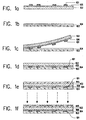
- FIG. 1 depicts the most general embodiment of the present invention and is described in detail hereinbelow:
- Fig. 1a ⁇ thick film resistors or capacitors known as passive components (101) are printed onto a conductive paste underprint (106) which is applied on a metallic foil (102) and then fired below the softening point of the metallic foil.
- Fig. 1b ⁇ a printed wiring board (PWB) (103) with an adhesive layer (104) coated on one side.
- PWB printed wiring board
- Fig. 1c the printed side of the fired metallic foil and the adhesive layer side of the PWB are laminated together.
- Fig. 1d the passive components are laminated in an inward direction, that is, they are embedded into the adhesive layer during the lamination process. This yields a relatively flat plane for the application of a photosensitive film.
- Fig. 1e ⁇ a photosensitive film is then laminated onto the metallic foil.
- Fig. 1f ⁇ the film is imagewise exposed to actinic radiation to define areas, which have been exposed.
- Fig. 1g ⁇ development is achieved by removal of the unexposed areas of the film, which leaves metallic foil exposed.
- Fig. 1i the circuit and the passive components are actualized in the same plane.
- the above process may, as referred to above, apply to double-sided builds.
- the metallic foils are those available in the industry.
- the preferred foils are copper, silver, gold, aluminum, nickel or iron foil with a thickness of about 0.01-100 ⁇ , preferably 2-75 ⁇ and most preferably 15-40 ⁇ .
- the thick film compositions known as pastes are utilized as the underprint and as the passive components.
- the resistor compositions are commercially available with RuO 2 , LaB 4 , SnO 2 , or TaN based thick film resistor pastes being preferred.
- the capacitor thick film compositions are commercially available with the barium titanate or titanium oxide thick film paste being preferred.
- thick film pastes are comprised of finely divided particles of glass, metal or other special function type particles (referred to as "solids") dispersed in polymers dissolved in a mixture of plasticizer, dispersing agent and organic solvent.
- the preferred pastes for the passive components are resistor pastes, which are well known in the industry, and commercially available although some blending may be needed to achieve desired resistances.
- the capacitor pastes are also commercially available but the preferred pastes which are printed on a copper system have an organic vehicle that exhibits good burn-out in a nitrogen atmosphere and an oxidizing component such as barium nitrate powder blended into the dielectric powder mixture.
- the solids are mixed with an essentially inert liquid medium (vehicle) by mechanical mixing using a planetary mixer, then dispersed on a three roll mill to form a paste-like composition having suitable consistency and rheology for screen printing.
- a paste-like composition having suitable consistency and rheology for screen printing.
- the latter is printed as a "thick film" on conventional ceramic substrates in the conventional manner.
- Any essentially inert liquid may be used as the vehicle.
- Various organic liquids with or without thickening and/or stabilizing agents and/or other common additives, may be used as the vehicle.
- organic liquids which can be used are the aliphatic alcohols, esters of such alcohols, for example, acetates and propionate, terpenes such as pine oil, terpineol and the like, solutions of resins such as the polymethacrylates of lower alcohols, solutions of ethyl cellulose in solvents such as pine oil and the monobutyl ether of ethylene glycol monoacetate and dibutyl carbitol.
- a preferred vehicle is based on ethyl cellulose resin and a solvent of texanol, a proprietary ester/alcohol from Eastman Chemicals (see Examples); alternatively, alpha-, beta-, and gamma terpineols (generally 85-92% alpha-terpineol containing 8-15% beta- and gamma-terpineols) also have superior properties when used as solvent for thick film inks, although poorer burnout properties than the texanol.
- the vehicle also may contain volatile liquids to promote fast setting after application to the substrate.
- the ratio of vehicle to solids in the dispersions can vary considerably and depends upon the manner in which the dispersion is to be applied and the kind of vehicle used. Normally to achieve good coverage, the dispersions will contain complementarily 50-91% solids and 50-9% vehicle, as described above.
- the compositions of the present invention may, of course, be modified by the addition of other materials, which do not affect its beneficial characteristics. Such formulations are well within the state of the art.
- the pastes are conveniently prepared on a three-roll mill.
- the viscosity of the pastes is typically within the following ranges when measured on a Brookfleld HBT viscometer at low, moderate and high shear rates: Shear Rate (sec -1 ) Viscosity (Pa *s) 0.2 100-5000 300-2000 Preferred 600-1500 Most Preferred 4 40-400 100-250 Preferred 120-200 Most Preferred 40 10-150 25-120 Preferred 50-100 Most Preferred
- the preferred organic layers used in this invention are the types of boards utilized in the printed-circuit board industry. Generally, they are made from high-pressure laminates. By definition, a laminate consists of layers of fibrous materials bonded together under heat and pressure with a thermosetting resin. Many times it is an electrical-grade paper bonded with phenolic or epoxy resin or a continuous-filament glass cloth bonded with an epoxy-resin system. More specifically, examples are:
- the adhesives should be electrically insulating.
- An epoxy, resin, acrylic or ceramic type adhesive may be used.
- the preferred thickness of the adhesive applied is about 0.04 to about 0.2 millimeters.
- the preferred adhesives are commercially available Vialux®, Pyralux® and Pyralux WA®.
- composition of the copper paste underprint follows: Texanol 15.00% Ethyl Cellulose 0.75% Glass A 0.60% Copper 83.50% Phosphate Wetting Agent 0.15%
- composition of Glass A is Composition of Glass A:
- the paste was prepared by techniques well known to those skilled in the art of thick film paste formulation and production.
- the glass was melted and fritted using standard techniques well known to those skilled in the art of glass production. Screen-printing was accomplished using standard screens (stainless steel mesh, 325 to 500 mesh screens). Thickness of the fired films on the copper foil was less than 10 microns, typically 8 to 9 microns.
- the material was mixed in a high shear high-speed mixer such as a Cowles, commonly used in the paint industry.
- a high shear high-speed mixer such as a Cowles, commonly used in the paint industry.
- the alumina was adequately dispersed in this manner, and no additional roll milling was used.
- Examples 1-6 are comparative and demonstrated without a copper paste underprint.
- Examples 7-12 exemplify the invention and are demonstrated with a copper paste underprint.
- the parts were printed using a 230-280 mesh screen; dried at 80°C; and fired on a nominal "30 minute" furnace profile (ten minutes peak at 900 degrees, with burnout ramp up to 20 minutes). Another 25 minutes is spent in unheated zones for a total residence time of 55 minutes in the tunnel kiln.
- the dielectric paste was printed onto a copper foil with an underprint, using two print/dry/fire sequences to lay down two dielectric layers, to minimize the effect of any pinholes.
- the parts were printed using a 400 mesh screen; dried at 80°C; and fired on a nominal "30 minute” furnace profile (ten minutes peak at 900 degrees, with burnout ramp up to 20 minutes). Another 25 minutes is spent in unheated zones for a total residence time of 55 minutes in the tunnel kiln.
- a low temperature silver paste is printed on the dielectrics, with a lead extending off the edge of the dielectric material. Since the copper does not affect the silver lead etch, it can be accessed after etching the copper off of it.
- the silver paste is fired in a furnace for ten minutes at 200°C. After firing, the material is ready to laminate, print, and etch. Usually, a copper pad is left on top of part of the silver lead to provide an attachment point.
- the composition for the dielectric paste is: Zicronium Oxide Powder 4.10% Glass "A” 6.10% Ethyl Cellulose 0.83% Eastman Texanol 17.63% Barium Titanate Powder 69.20% Barium Nitrate Powder 0.84% Phosphate Wetting Agent 0.40%
- Glass “A” is composed of: Germanium Oxide 21.5% Lead Tetraoxide 78.5%
- Texanol is a proprietary ester/alcohol from Eastman; the ethyl cellulose is grade "T-200" from Hercules; and the phosphate wetting agent is tridecyl phosphate from AKZO. Powders are ground by processes familiar to those skilled in the art of formulation of thick film inks; the glass is also prepared using commonly used procedures. Organic and inorganic portions of the formula are mixed and roll milled to produce a thick film printing ink of viscosity suitable for screen-printing.
- composition of the silver paste is as follows: 5 micron flake silver 48.2% 1-2 micron silver 26.8% 0.6 to 0.8 micron silver 3.6% Ethyl Cellulose resin 1.4% Texanol 20.0%
- the ethyl cellulose is T-200 grade, from Hercules; the Texanol is an alcohol/ester solvent from Eastman. Silver paste was prepared using techniques well known to formulators skilled in thick film art.
Landscapes
- Engineering & Computer Science (AREA)
- Microelectronics & Electronic Packaging (AREA)
- Manufacturing & Machinery (AREA)
- Parts Printed On Printed Circuit Boards (AREA)
- Manufacturing Of Printed Wiring (AREA)
Abstract
Description
| Shear Rate (sec-1) | Viscosity (Pa *s) |
| 0.2 | 100-5000 |
| 300-2000 | Preferred |
| 600-1500 | Most Preferred |
| 4 | 40-400 |
| 100-250 | Preferred |
| 120-200 | Most Preferred |
| 40 | 10-150 |
| 25-120 | Preferred |
| 50-100 | Most Preferred |
| Texanol | 15.00% |
| Ethyl Cellulose | 0.75% |
| Glass A | 0.60% |
| Copper | 83.50% |
| Phosphate Wetting Agent | 0.15% |
| Silica | 9.4% |
| B2O3 | 12.2% |
| Lead Oxide | 65.9% |
| Cadmium Oxide | 6.7% |
| Sodium Fluoride | 3.2% |
| Aluminum Oxide | 0.2% |
| Ingredient | Per Cent |
| Alumina Powder (Bayer Process, ∼2 micron) | 55.0% |
| Solvent (dibutyl carbitol) | 16.0% |
| Resin (bisphenol-F. Shell #862) | 25.3% |
| Cyanoguanidine (Dyhard 100SF, SKW Trostberg) | 2.4% |
| Thermal Initiator (UR-150, SKW Trostberg) (Toluene2,4-bis(N,N-dimethylcarbamine)) | 1.3% |
| Without Copper Paste Underprint | With Copper Paste Underprint | ||
| 1. | No underprint layer | 1. | Screen Print/Dry Copper Underprint Layer |
| 2. | No firing | 2. | Fire Copper Underprint Layer |
| 3. | Print/Dry Resistor Paste | 3. | Print/Dry Resistor Paste |
| 4. | Fire Resistor Paste | 4. | Fire Resistor Paste |
| 5. | Vacuum Laminate Fired Parts of PWB which is coated on the converging side with Pryalux Adhesive | 5. | Vacuum Laminate Fired Parts to PWB which is coated on the converging side with Pyralux Adhesive |
| 6. | Microetch to Accept Riston | 6. | Microetch to Accept Riston |
| 7. | Laminate Riston | 7. | Laminate Riston |
| 8. | Expose Conductor Pattern on Riston | 8. | Expose Conductor Pattern on Riston |
| 9. | Develop/etch/strip boards | 9. | Develop/etch/strip boards |
| 10. | Print a curable epoxy encapsulant over the patterned resistors | 10. | Print a curable epoxy encapsulant over the patterned resistors |
| Resistors Printed without Cu Paste Underprint - 10Kohm, R, Average, and CV 10,000 Ohm Lanthanum boride resistor paste printed with Screen-Using Pyralux Adhesive | |||||||
| Ex. 1 | Ex. 2 | Ex. 3 | Ex. 4 | Ex. 5 | Ex. 6 | ||
| 26.65 | 27.92 | 20.57 | Open | 19.87 | Open | R | V |
| 27.58 | 22.16 | 21.44 | 20.69 | 20.93 | 22.16 | E | A |
| 26.91 | 152.8* | 22.62 | 29.45 | 24.1 | 28.9 | S | L |
| 33.73 | 28.11 | 25.76 | 24.82 | 28.8 | 26.3 | I | U |
| 31.58 | 38.2 | 26.4 | 36.8 | 28.1 | 34.2 | S | E |
| 32.6 | 36.7 | 27.62 | 32.5 | 31.06 | 34.3 | T | S |
| 33.5 | 27.31 | 476* | 27.27 | 31.6 | 32.2 | O | |
| 31.3 | 27.76 | 710* | 32.5 | 33.1 | 34.1 | R | |
| 30.48125 | 29.73714 | 24.06833 | 29.14714 | 27.195 | 30.30857 | Average | |
| 2.973298 | 5.675446 | 2.903683 | 5.399265 | 5.001303 | 4.716621 | Standard Deviation |
| Resistors with Underprint of Cu Paste - 10kOhm, Resistance, Ave. and CV (20 x 20 resistors) | |||||||
| Ex. 7 | Ex. 8 | Ex. 9 | Ex. 10 | Ex. 11 | Ex. 12 | ||
| 24.3 | 21.1 | 21.9 | 17.9 | 22.3 | 20.9 | R | V |
| Open | 21.1 | 21.9 | 18.5 | 21 | 21.5 | E | A |
| 20.8 | 21.3 | 19.7 | 19.1 | 19 | 21.5 | S | L |
| 21.4 | 21 | 19.4 | 19.4 | 17.3 | 21.2 | I | U |
| 22.8 | 20 | 21.8 | 22.4 | 13.8 | 20.5 | S | E |
| 22.7 | 22 | 21.4 | 21.1 | 15.5 | 21 | T | S |
| 20.9 | 21 | 20.8 | 17.4 | 17.1 | 21.6 | O | |
| 17.6 | 17.6 | 19.6 | 15.9 | 20.1 | 19.7 | R | |
| 22.15 | 21.07143 | 20.98571 | 19.4 | 18 | 21.17143 | Average | |
| 1.363452 | 0.587975 | 1.0574 | 1.781385 | 2.991098 | 0.398808 | Standard Deviation |
| Zicronium Oxide Powder | 4.10% |
| Glass "A" | 6.10% |
| Ethyl Cellulose | 0.83% |
| Eastman Texanol | 17.63% |
| Barium Titanate Powder | 69.20% |
| Barium Nitrate Powder | 0.84% |
| Phosphate Wetting Agent | 0.40% |
| Germanium Oxide | 21.5% |
| Lead Tetraoxide | 78.5% |
| 5 micron flake silver | 48.2% |
| 1-2 micron silver | 26.8% |
| 0.6 to 0.8 micron silver | 3.6% |
| Ethyl Cellulose resin | 1.4% |
| Texanol | 20.0% |
Claims (10)
- A method of embedding thick film passive components comprising the following steps:A. applying as an underprint a conductor paste onto a flexible metallic substrate;B. firing the article found in step A.;C. applying at least one resistor paste onto the underprint;D. firing the article found in step C.;E. applying the fired paste side of the article found in step D. onto at least one side of an organic layer which is at least partially coated with an adhesive layer wherein the fired paste side of the article is embedded into the adhesive layer.
- A method of embedding thick film passive components comprising the following steps:A. applying as an underprint a first conductor paste onto a flexible metallic substrate;B. firing the article found in step A.;C. applying at least one dielectric paste onto the underprint;D. firing the article found in step C.;E. applying a second conductor paste onto the fired pastes;F. firing the article found in step E.;G. applying the fired paste side of the article found in step F. onto at least one side of an organic layer which is at least partially coated with an adhesive layer wherein the fired paste side of the article is embedded into the adhesive layer.
- A method of embedding thick film passive components comprising the following sequential steps:A. applying as an underprint a first conductor paste onto a flexible metallic substrate;B. firing the article found in step A;C. applying at least one dielectric paste onto the underprint;D. firing the article found in step C.;E. applying a thermoset thick film conductor onto the fired pastes;F. curing the article found in step E.;G. applying the cured paste side of the article found in step F. onto at least one side of an organic layer which is at least partially coated with an adhesive layer wherein the cured paste side of the article is embedded into the adhesive layer.
- The method of Claim 2 or 3 wherein the step of applying at least one dielectric paste further comprises applying at least one resistor paste onto the underprint.
- The method of Claim 2 or 3 wherein the step of applying at least one dielectric paste further comprises applying at least one resistor paste onto the dielectric paste.
- The method according to either of Claim 1, 2 or 3 wherein the firing steps are performed below the softening or melting point of the metallic substrate.
- The method of Claim 1, 2 or 3 further comprises an encapsulant.
- The method of Claims 1, 2 or 3 wherein the underprint is a conductor paste comprising the same type of metal as found in the metallic substrate.
- The method of Claim 2 or 3 wherein the dielectric paste contains an oxidizing agent.
- A buried passive component formed in accordance with the method of Claim 1, 2 or 3.
Applications Claiming Priority (2)
| Application Number | Priority Date | Filing Date | Title |
|---|---|---|---|
| US09/419,681 US6317023B1 (en) | 1999-10-15 | 1999-10-15 | Method to embed passive components |
| US419681 | 1999-10-15 |
Publications (3)
| Publication Number | Publication Date |
|---|---|
| EP1093327A2 true EP1093327A2 (en) | 2001-04-18 |
| EP1093327A3 EP1093327A3 (en) | 2003-12-10 |
| EP1093327B1 EP1093327B1 (en) | 2006-12-20 |
Family
ID=23663295
Family Applications (1)
| Application Number | Title | Priority Date | Filing Date |
|---|---|---|---|
| EP00114762A Expired - Lifetime EP1093327B1 (en) | 1999-10-15 | 2000-07-10 | An improved method to embed passive components |
Country Status (6)
| Country | Link |
|---|---|
| US (2) | US6317023B1 (en) |
| EP (1) | EP1093327B1 (en) |
| JP (1) | JP3556164B2 (en) |
| KR (1) | KR100377309B1 (en) |
| DE (1) | DE60032438T2 (en) |
| TW (1) | TWI240602B (en) |
Cited By (8)
| Publication number | Priority date | Publication date | Assignee | Title |
|---|---|---|---|---|
| EP1261241A1 (en) * | 2001-05-17 | 2002-11-27 | Shipley Co. L.L.C. | Resistor and printed wiring board embedding those resistor |
| EP1355519A3 (en) * | 2002-02-15 | 2003-11-05 | E.I. Dupont De Nemours And Company | An improved method to embed thick film components |
| WO2004056160A1 (en) * | 2002-12-13 | 2004-07-01 | E.I. Du Pont De Nemours And Company | Printed wiring boards having low inductance embedded capacitors and methods of making same |
| EP1578179A3 (en) * | 2004-03-16 | 2006-05-03 | E.I. du Pont de Nemours and Company | Thick-film dielectric and conductive compositions |
| EP1737283A1 (en) * | 2005-06-20 | 2006-12-27 | E.I.Du pont de nemours and company | Embedded capacitors, electronic devices comprising such capacitors and methods for making the same |
| US7531416B2 (en) | 2005-12-21 | 2009-05-12 | E. I. Du Pont De Nemours And Company | Thick film capacitors on ceramic interconnect substrates |
| US7688569B2 (en) | 2004-03-16 | 2010-03-30 | E. I. Du Pont De Nemours And Company | Thick-film dielectric and conductive compositions |
| WO2016007351A1 (en) * | 2014-07-11 | 2016-01-14 | E. I. Du Pont De Nemours And Company | Flowable compositions with low temperature curing to form thermally conductive pathways in electronics type applications and methods relating thereto |
Families Citing this family (59)
| Publication number | Priority date | Publication date | Assignee | Title |
|---|---|---|---|---|
| US6338809B1 (en) | 1997-02-24 | 2002-01-15 | Superior Micropowders Llc | Aerosol method and apparatus, particulate products, and electronic devices made therefrom |
| EP1007308B1 (en) | 1997-02-24 | 2003-11-12 | Superior Micropowders LLC | Aerosol method and apparatus, particulate products, and electronic devices made therefrom |
| US6621012B2 (en) * | 2001-02-01 | 2003-09-16 | International Business Machines Corporation | Insertion of electrical component within a via of a printed circuit board |
| US6576489B2 (en) * | 2001-05-07 | 2003-06-10 | Applied Materials, Inc. | Methods of forming microstructure devices |
| US6696906B1 (en) * | 2001-05-30 | 2004-02-24 | Hewlett-Packard Development Company, L.P. | Low dielectric loss signal line having a conductive trace supported by filaments |
| TW518616B (en) * | 2001-06-01 | 2003-01-21 | Phoenix Prec Technology Corp | Method of manufacturing multi-layer circuit board with embedded passive device |
| EP2315510A3 (en) * | 2001-06-05 | 2012-05-02 | Dai Nippon Printing Co., Ltd. | Wiring board provided with passive element |
| JP4515477B2 (en) * | 2001-06-05 | 2010-07-28 | 大日本印刷株式会社 | Method for manufacturing wiring board with passive element |
| US20030108664A1 (en) * | 2001-10-05 | 2003-06-12 | Kodas Toivo T. | Methods and compositions for the formation of recessed electrical features on a substrate |
| US7524528B2 (en) | 2001-10-05 | 2009-04-28 | Cabot Corporation | Precursor compositions and methods for the deposition of passive electrical components on a substrate |
| US7629017B2 (en) | 2001-10-05 | 2009-12-08 | Cabot Corporation | Methods for the deposition of conductive electronic features |
| US6951666B2 (en) * | 2001-10-05 | 2005-10-04 | Cabot Corporation | Precursor compositions for the deposition of electrically conductive features |
| US7083850B2 (en) * | 2001-10-18 | 2006-08-01 | Honeywell International Inc. | Electrically conductive thermal interface |
| JP4763237B2 (en) | 2001-10-19 | 2011-08-31 | キャボット コーポレイション | Method for manufacturing a conductive electronic component on a substrate |
| US7553512B2 (en) | 2001-11-02 | 2009-06-30 | Cabot Corporation | Method for fabricating an inorganic resistor |
| US20050063135A1 (en) * | 2003-09-18 | 2005-03-24 | Borland William J. | High tolerance embedded capacitors |
| US20040108134A1 (en) * | 2002-10-11 | 2004-06-10 | Borland William J. | Printed wiring boards having low inductance embedded capacitors and methods of making same |
| US20040099999A1 (en) * | 2002-10-11 | 2004-05-27 | Borland William J. | Co-fired capacitor and method for forming ceramic capacitors for use in printed wiring boards |
| US6897761B2 (en) * | 2002-12-04 | 2005-05-24 | Cts Corporation | Ball grid array resistor network |
| US20040231885A1 (en) * | 2003-03-07 | 2004-11-25 | Borland William J. | Printed wiring boards having capacitors and methods of making thereof |
| US7274100B2 (en) * | 2003-06-23 | 2007-09-25 | International Rectifier Corporation | Battery protection circuit with integrated passive components |
| JP4047243B2 (en) * | 2003-08-07 | 2008-02-13 | 株式会社日立製作所 | Organic / inorganic oxide mixed thin film, electronic substrate with built-in passive element using the same, and method for producing organic / inorganic oxide mixed thin film |
| US7042331B2 (en) * | 2003-08-12 | 2006-05-09 | Delphi Technologies, Inc. | Fabrication of thick film electrical components |
| US7178229B2 (en) * | 2003-11-20 | 2007-02-20 | E. I. Du Pont De Nemours And Company | Method of making interlayer panels |
| TWI265534B (en) * | 2003-12-31 | 2006-11-01 | Polytronics Technology Corp | Over-current protection apparatus |
| US20050204864A1 (en) * | 2004-03-16 | 2005-09-22 | Borland William J | Thick-film dielectric and conductive compositions |
| US20050208706A1 (en) * | 2004-03-17 | 2005-09-22 | Blazek Roy J | Method of creating multi-layered monolithic circuit structure containing integral buried and trimmed components |
| US20070019789A1 (en) * | 2004-03-29 | 2007-01-25 | Jmar Research, Inc. | Systems and methods for achieving a required spot says for nanoscale surface analysis using soft x-rays |
| US7100277B2 (en) * | 2004-07-01 | 2006-09-05 | E. I. Du Pont De Nemours And Company | Methods of forming printed circuit boards having embedded thick film capacitors |
| TWI251455B (en) * | 2004-07-06 | 2006-03-11 | Advanced Semiconductor Eng | A manufacturing method of a multi-layer circuit board with embedded passive components |
| US7342804B2 (en) * | 2004-08-09 | 2008-03-11 | Cts Corporation | Ball grid array resistor capacitor network |
| US20060120015A1 (en) * | 2004-12-02 | 2006-06-08 | Borland William J | Thick-film capacitors, embedding thick-film capacitors inside printed circuit boards, and methods of forming such capacitors and printed circuit boards |
| US20060141225A1 (en) * | 2004-12-28 | 2006-06-29 | Borland William J | Oxygen doped firing of barium titanate on copper foil |
| KR20070086706A (en) * | 2004-12-28 | 2007-08-27 | 니뽄 도쿠슈 도교 가부시키가이샤 | Wiring board and manufacturing method of the wiring board |
| US7824466B2 (en) | 2005-01-14 | 2010-11-02 | Cabot Corporation | Production of metal nanoparticles |
| US8167393B2 (en) | 2005-01-14 | 2012-05-01 | Cabot Corporation | Printable electronic features on non-uniform substrate and processes for making same |
| US7533361B2 (en) | 2005-01-14 | 2009-05-12 | Cabot Corporation | System and process for manufacturing custom electronics by combining traditional electronics with printable electronics |
| US8383014B2 (en) | 2010-06-15 | 2013-02-26 | Cabot Corporation | Metal nanoparticle compositions |
| WO2006076606A2 (en) | 2005-01-14 | 2006-07-20 | Cabot Corporation | Optimized multi-layer printing of electronics and displays |
| WO2006076612A2 (en) | 2005-01-14 | 2006-07-20 | Cabot Corporation | A process for manufacturing application specific printable circuits (aspc’s) and other custom electronic devices |
| US20060282999A1 (en) * | 2005-06-20 | 2006-12-21 | Diptarka Majumdar | Electrodes, inner layers, capacitors and printed wiring boards and methods of making thereof - part II |
| US7456459B2 (en) * | 2005-10-21 | 2008-11-25 | Georgia Tech Research Corporation | Design of low inductance embedded capacitor layer connections |
| US7504706B2 (en) * | 2005-10-21 | 2009-03-17 | E. I. Du Pont De Nemours | Packaging having an array of embedded capacitors for power delivery and decoupling in the mid-frequency range and methods of forming thereof |
| US7705423B2 (en) | 2005-10-21 | 2010-04-27 | Georgia Tech Research Corporation | Device having an array of embedded capacitors for power delivery and decoupling of high speed input/output circuitry of an integrated circuit |
| US20070210426A1 (en) * | 2006-03-07 | 2007-09-13 | Gerber Mark A | Gold-bumped interposer for vertically integrated semiconductor system |
| US20070236859A1 (en) * | 2006-04-10 | 2007-10-11 | Borland William J | Organic encapsulant compositions for protection of electronic components |
| US20070244267A1 (en) * | 2006-04-10 | 2007-10-18 | Dueber Thomas E | Hydrophobic crosslinkable compositions for electronic applications |
| US20070291440A1 (en) * | 2006-06-15 | 2007-12-20 | Dueber Thomas E | Organic encapsulant compositions based on heterocyclic polymers for protection of electronic components |
| JP2010512449A (en) * | 2006-12-12 | 2010-04-22 | イー・アイ・デュポン・ドウ・ヌムール・アンド・カンパニー | Crystalline mounting medium |
| WO2008073409A2 (en) * | 2006-12-12 | 2008-06-19 | E. I. Du Pont De Nemours And Company | Composite organic encapsulants |
| US20080160173A1 (en) * | 2006-12-27 | 2008-07-03 | Nokia Corporation | Component Moulding Process |
| KR101002500B1 (en) * | 2007-02-06 | 2010-12-17 | 이비덴 가부시키가이샤 | Printed wiring board and manufacturing method of the printed wiring board |
| US8357753B2 (en) | 2007-07-18 | 2013-01-22 | Cda Processing Limited Liability Company | Screen-printable encapsulants based on polyhydroxyamides that thermally convert to polybenzoxazoles |
| US8270145B2 (en) * | 2007-12-04 | 2012-09-18 | Cda Processing Limited Liability Company | Screen-printable encapsulants based on soluble polybenzoxazoles |
| TWI600354B (en) * | 2014-09-03 | 2017-09-21 | 光頡科技股份有限公司 | Micro-resistance structure with high bending strength, manufacturing method thereof |
| WO2017188446A1 (en) * | 2016-04-28 | 2017-11-02 | シャープ株式会社 | Conductive paste, electrode connection structure, and electrode connection structure production method |
| TWI713424B (en) * | 2018-10-15 | 2020-12-11 | 鼎展電子股份有限公司 | Copper film with buried film resistor and printed circuit board having the same |
| US20220119315A1 (en) * | 2020-02-05 | 2022-04-21 | Ferro Corporation | M7 LTCC-Silver System And Related Dielectric Compositions For High Frequency Applications |
| EP4464771B1 (en) * | 2022-03-17 | 2026-06-24 | PHC Holdings Corporation | Incubation device and incubation system |
Family Cites Families (15)
| Publication number | Priority date | Publication date | Assignee | Title |
|---|---|---|---|---|
| FR1130057A (en) * | 1954-05-04 | 1957-01-30 | Norton And Gregory Ltd | Improvements to circuits and electrical elements obtained by printing |
| GB1258660A (en) * | 1969-12-19 | 1971-12-30 | ||
| US4180608A (en) * | 1977-01-07 | 1979-12-25 | Del Joseph A | Process for making multi-layer printed circuit boards, and the article resulting therefrom |
| JPS5469768A (en) * | 1977-11-14 | 1979-06-05 | Nitto Electric Ind Co | Printing circuit substrate with resistance |
| DE3322382A1 (en) * | 1983-06-22 | 1985-01-10 | Preh, Elektrofeinmechanische Werke Jakob Preh Nachf. Gmbh & Co, 8740 Bad Neustadt | METHOD FOR PRODUCING PRINTED CIRCUITS |
| US4724040A (en) * | 1986-01-14 | 1988-02-09 | Asahi Chemical Research Laboratory Co., Ltd. | Method for producing electric circuits on a base boad |
| JPH0265194A (en) * | 1988-08-30 | 1990-03-05 | Ibiden Co Ltd | Manufacture of printed wiring board with thick film element |
| JPH02153589A (en) | 1988-12-05 | 1990-06-13 | Ibiden Co Ltd | Printed wiring board provided with thick film element |
| JP2707903B2 (en) | 1992-01-28 | 1998-02-04 | 日本電気株式会社 | Manufacturing method of multilayer printed wiring board |
| JPH0722741A (en) * | 1993-07-01 | 1995-01-24 | Japan Gore Tex Inc | Coverlay film and coverlay film coated circuit board |
| US5362534A (en) * | 1993-08-23 | 1994-11-08 | Parlex Corporation | Multiple layer printed circuit boards and method of manufacture |
| JP3372636B2 (en) * | 1994-03-16 | 2003-02-04 | アルプス電気株式会社 | Manufacturing method of resistive substrate |
| US5652055A (en) * | 1994-07-20 | 1997-07-29 | W. L. Gore & Associates, Inc. | Matched low dielectric constant, dimensionally stable adhesive sheet |
| IT235724Y1 (en) | 1995-11-06 | 2000-07-12 | Siv Soc Italiana Vetro | GASKET PERFECTLY PARTICULARLY SUITABLE FOR APPLICATION ON GLASS FOR VEHICLES |
| JP3944791B2 (en) | 1997-03-06 | 2007-07-18 | ラミナ セラミクス, インコーポレイテッド | Ceramic multilayer printed circuit board |
-
1999
- 1999-10-15 US US09/419,681 patent/US6317023B1/en not_active Expired - Fee Related
-
2000
- 2000-06-13 TW TW089111491A patent/TWI240602B/en not_active IP Right Cessation
- 2000-07-10 EP EP00114762A patent/EP1093327B1/en not_active Expired - Lifetime
- 2000-07-10 DE DE60032438T patent/DE60032438T2/en not_active Expired - Lifetime
- 2000-10-13 KR KR10-2000-0060197A patent/KR100377309B1/en not_active Expired - Fee Related
- 2000-10-16 JP JP2000315952A patent/JP3556164B2/en not_active Expired - Fee Related
-
2001
- 2001-04-18 US US09/836,921 patent/US20020028284A1/en not_active Abandoned
Cited By (9)
| Publication number | Priority date | Publication date | Assignee | Title |
|---|---|---|---|---|
| EP1261241A1 (en) * | 2001-05-17 | 2002-11-27 | Shipley Co. L.L.C. | Resistor and printed wiring board embedding those resistor |
| EP1355519A3 (en) * | 2002-02-15 | 2003-11-05 | E.I. Dupont De Nemours And Company | An improved method to embed thick film components |
| WO2004056160A1 (en) * | 2002-12-13 | 2004-07-01 | E.I. Du Pont De Nemours And Company | Printed wiring boards having low inductance embedded capacitors and methods of making same |
| EP1578179A3 (en) * | 2004-03-16 | 2006-05-03 | E.I. du Pont de Nemours and Company | Thick-film dielectric and conductive compositions |
| US7688569B2 (en) | 2004-03-16 | 2010-03-30 | E. I. Du Pont De Nemours And Company | Thick-film dielectric and conductive compositions |
| EP1737283A1 (en) * | 2005-06-20 | 2006-12-27 | E.I.Du pont de nemours and company | Embedded capacitors, electronic devices comprising such capacitors and methods for making the same |
| US7531416B2 (en) | 2005-12-21 | 2009-05-12 | E. I. Du Pont De Nemours And Company | Thick film capacitors on ceramic interconnect substrates |
| WO2016007351A1 (en) * | 2014-07-11 | 2016-01-14 | E. I. Du Pont De Nemours And Company | Flowable compositions with low temperature curing to form thermally conductive pathways in electronics type applications and methods relating thereto |
| US9840651B2 (en) | 2014-07-11 | 2017-12-12 | E I Du Pont De Nemours And Company | Flowable compositions with low temperature curing to form thermally conductive pathways in electronics type applications and methods relating thereto |
Also Published As
| Publication number | Publication date |
|---|---|
| JP2001160672A (en) | 2001-06-12 |
| EP1093327B1 (en) | 2006-12-20 |
| US20020028284A1 (en) | 2002-03-07 |
| JP3556164B2 (en) | 2004-08-18 |
| KR20010070138A (en) | 2001-07-25 |
| US6317023B1 (en) | 2001-11-13 |
| KR100377309B1 (en) | 2003-03-26 |
| EP1093327A3 (en) | 2003-12-10 |
| DE60032438T2 (en) | 2007-10-04 |
| TWI240602B (en) | 2005-09-21 |
| DE60032438D1 (en) | 2007-02-01 |
Similar Documents
| Publication | Publication Date | Title |
|---|---|---|
| US6317023B1 (en) | Method to embed passive components | |
| US6860000B2 (en) | Method to embed thick film components | |
| KR100553635B1 (en) | Co-fired ceramic capacitor and method for forming ceramic capacitor for use in printed wiring boards | |
| US7701052B2 (en) | Power core devices | |
| KR100687689B1 (en) | Printed wiring board comprising an innerlayer panel, a method of making the innerlayer panel and an innerlayer panel | |
| US20040108134A1 (en) | Printed wiring boards having low inductance embedded capacitors and methods of making same | |
| WO2004056160A1 (en) | Printed wiring boards having low inductance embedded capacitors and methods of making same | |
| US7186307B2 (en) | Method for manufacturing a ceramic multilayer circuit board | |
| JP2002198654A (en) | Wiring board with built-in electric element and method of manufacturing the same | |
| US9307649B2 (en) | Mixed-metal system conductors for use in low-temperature co-fired ceramic circuits and devices | |
| CN116640549A (en) | Cover film composition applicable to embedded capacitor, cover film, embedded capacitor, circuit board and preparation method thereof | |
| JPH10200227A (en) | Method of manufacturing via-hole conductor for low-temperature fired ceramic substrate and conductor paste for via-hole | |
| JPH08191177A (en) | Via conductive paste and method of manufacturing the same | |
| JPH0593159A (en) | Ink composition | |
| JPH10242609A (en) | Ceramic circuit board and method of manufacturing the same | |
| JPH0218591B2 (en) |
Legal Events
| Date | Code | Title | Description |
|---|---|---|---|
| PUAI | Public reference made under article 153(3) epc to a published international application that has entered the european phase |
Free format text: ORIGINAL CODE: 0009012 |
|
| AK | Designated contracting states |
Kind code of ref document: A2 Designated state(s): AT BE CH CY DE DK ES FI FR GB GR IE IT LI LU MC NL PT SE |
|
| AX | Request for extension of the european patent |
Free format text: AL;LT;LV;MK;RO;SI |
|
| PUAL | Search report despatched |
Free format text: ORIGINAL CODE: 0009013 |
|
| AK | Designated contracting states |
Kind code of ref document: A3 Designated state(s): AT BE CH CY DE DK ES FI FR GB GR IE IT LI LU MC NL PT SE |
|
| AX | Request for extension of the european patent |
Extension state: AL LT LV MK RO SI |
|
| 17P | Request for examination filed |
Effective date: 20040414 |
|
| 17Q | First examination report despatched |
Effective date: 20040525 |
|
| AKX | Designation fees paid |
Designated state(s): DE FR GB |
|
| GRAP | Despatch of communication of intention to grant a patent |
Free format text: ORIGINAL CODE: EPIDOSNIGR1 |
|
| GRAS | Grant fee paid |
Free format text: ORIGINAL CODE: EPIDOSNIGR3 |
|
| GRAA | (expected) grant |
Free format text: ORIGINAL CODE: 0009210 |
|
| AK | Designated contracting states |
Kind code of ref document: B1 Designated state(s): DE FR GB |
|
| REG | Reference to a national code |
Ref country code: GB Ref legal event code: FG4D |
|
| REF | Corresponds to: |
Ref document number: 60032438 Country of ref document: DE Date of ref document: 20070201 Kind code of ref document: P |
|
| ET | Fr: translation filed | ||
| PLBE | No opposition filed within time limit |
Free format text: ORIGINAL CODE: 0009261 |
|
| STAA | Information on the status of an ep patent application or granted ep patent |
Free format text: STATUS: NO OPPOSITION FILED WITHIN TIME LIMIT |
|
| 26N | No opposition filed |
Effective date: 20070921 |
|
| PGFP | Annual fee paid to national office [announced via postgrant information from national office to epo] |
Ref country code: DE Payment date: 20100707 Year of fee payment: 11 Ref country code: FR Payment date: 20100805 Year of fee payment: 11 |
|
| PGFP | Annual fee paid to national office [announced via postgrant information from national office to epo] |
Ref country code: GB Payment date: 20100707 Year of fee payment: 11 |
|
| GBPC | Gb: european patent ceased through non-payment of renewal fee |
Effective date: 20110710 |
|
| REG | Reference to a national code |
Ref country code: FR Ref legal event code: ST Effective date: 20120330 |
|
| PG25 | Lapsed in a contracting state [announced via postgrant information from national office to epo] |
Ref country code: FR Free format text: LAPSE BECAUSE OF NON-PAYMENT OF DUE FEES Effective date: 20110801 Ref country code: DE Free format text: LAPSE BECAUSE OF NON-PAYMENT OF DUE FEES Effective date: 20120201 |
|
| REG | Reference to a national code |
Ref country code: DE Ref legal event code: R119 Ref document number: 60032438 Country of ref document: DE Effective date: 20120201 |
|
| PG25 | Lapsed in a contracting state [announced via postgrant information from national office to epo] |
Ref country code: GB Free format text: LAPSE BECAUSE OF NON-PAYMENT OF DUE FEES Effective date: 20110710 |