EP1091214A2 - Verfahren und Vorrichtung zur Aufbereitung von Messsignalen - Google Patents
Verfahren und Vorrichtung zur Aufbereitung von Messsignalen Download PDFInfo
- Publication number
- EP1091214A2 EP1091214A2 EP00119252A EP00119252A EP1091214A2 EP 1091214 A2 EP1091214 A2 EP 1091214A2 EP 00119252 A EP00119252 A EP 00119252A EP 00119252 A EP00119252 A EP 00119252A EP 1091214 A2 EP1091214 A2 EP 1091214A2
- Authority
- EP
- European Patent Office
- Prior art keywords
- signal
- frequency
- offset
- sum
- samples
- Prior art date
- Legal status (The legal status is an assumption and is not a legal conclusion. Google has not performed a legal analysis and makes no representation as to the accuracy of the status listed.)
- Granted
Links
Images


Classifications
-
- G—PHYSICS
- G01—MEASURING; TESTING
- G01R—MEASURING ELECTRIC VARIABLES; MEASURING MAGNETIC VARIABLES
- G01R19/00—Arrangements for measuring currents or voltages or for indicating presence or sign thereof
- G01R19/25—Arrangements for measuring currents or voltages or for indicating presence or sign thereof using digital measurement techniques
Definitions
- the present invention relates to a method for processing a measurement signal.
- Measuring devices such as sensors, bridge circuits or the like, have the disadvantage that it gives the measurement signal that is of interest to the user a first offset signal superimpose, which is due to mechanical sensitivity of the measuring device, inaccuracies in the manufacturing technology of the measuring devices and / or through the electronics.
- the value of this offset signal is often unknown to the user and can also be vary in time.
- Some measuring devices such as Hall sensors or resistance bridge circuits can are controlled so that the offset is alternately added to the measurement signal and from Measurement signal is subtracted.
- the offset of the measurement signal is therefore not a direct signal but rather as an alternating signal, ideally superimposed as a rectangular alternating signal.
- the Control of the sensors or bridge circuits in this way is called “choppers" designated.
- the frequency with which the offset signal changes its sign is called as “chopper frequency”.
- the chopper frequency is usually chosen much higher than the maximum frequency of the measurement signal of interest, so that there is the possibility of the high-frequency offset signal separated from the measurement signal by means of a low-pass filter and thereby an offset-free one Obtain measurement signal.
- a disadvantage of this procedure is the high level of circuitry involved in the filtering of the signal and the fact that filtering usually results in a new one Offset is generated.
- the invention provides a method for processing a measurement signal, the an alternating offset signal is superimposed, according to the features of claim 1 in front.
- a measuring device such as a Hall sensor or Resistor bridge, supplied sum signal, which consists of a measurement signal and a Offset signal of a first frequency (chopper frequency) composed for provision sampled in time with a second frequency, the second frequency being a Is a multiple of the first frequency.
- the measurement values of the Measurement signal the mean of at least two samples formed by samples of the sum signal at intervals of half a period of the first frequency or at intervals of odd multiples of half the period of the first frequency were.
- the sampling of the sum signal in time with the second frequency which is a multiple of first frequency, and the provision of the measured values by averaging in time with the second frequency is used to improve the temporal resolution of the measurement signal, in particular is required for applications in which the zero crossing of the measurement signal should be evaluated.
- the sum signal from the measurement signal is provided and amplify offset signal before sampling. This reinforcement is required if the amplitude of the first sum signal, i.e. the output signal of the measuring device, is too small for further processing by sampling and averaging. To the amplification of the first sum signal, from which a second sum signal results, the second sum signal is sampled and the mean of at least two samples educated.
- the sign of the input signal of the amplifier is periodic Interchanging time intervals in time with a third frequency or the phase of the Rotate input signal by 180 ° in time with the third frequency. This causes that the second offset of the amplifier in the periods in which the sign of the Input signal is interchanged, is added to the negative input signal and in the periods in which the sign of the input signal is maintained at positive input signal is added.
- the rotation of the sign of the input signal at periodic intervals in time the third frequency is reversed by swapping the sign of the Output signal at periodic intervals in time with the third frequency, the Swap the sign of the output signal in phase with swapping the
- the input signal is signed. This gives an output signal that corresponds to the input signal amplified with a gain factor of the amplifier, which the second offset of the amplifier as a rectangular signal of the third frequency is superimposed.
- the procedure described is called chopping the amplifier with the third Designated frequency.
- the third frequency of the amplifier offset signal preferably corresponds to the first frequency of the offset signal of the measuring arrangement or is an even multiple of this first Frequency. This ensures that during the subsequent sampling and averaging the value of the second offset of the amplifier is also eliminated.
- the third frequency i.e. the chopper frequency of the amplifier
- the chopper frequency of the measuring device is at the output of the amplifier a signal that corresponds to the amplified measurement signal, that a total offset signal is superimposed on the first frequency, the amplitude of the total offset signal from the amplified first offset signal of the measuring arrangement and the second Offset signal of the amplifier results.
- This total offset signal is determined by that of the sampling following averaging eliminated.
- the gain of the amplifier is preferably regulated according to the amplitude of the input signal, so that the amplitude of the output signal of the amplifier essentially remains constant regardless of the amplitude of the input signal.
- the invention further relates to a device for processing a measurement signal according to claim 8.
- the device has a scanning device for scanning one of the sum signal dependent input signal in time with a second frequency to provide a sequence of samples on.
- a device for averaging is connected downstream of the scanning device, which is the sequence of the sample values for providing measured values by addition or forming the average of at least two samples are supplied.
- the device for averaging preferably has a memory for storage of samples and an adder for adding two stored values or for addition a storage value and a sample value present at the input of the device.
- the number of memory cells in the memory preferably corresponds to the number of samples, those within half a period of the first frequency of the first offset signal be preserved.
- Another embodiment of the invention provides memory cells for storing the Provide samples of an entire period of the offset signal. For averaging in each case the values of two memory cells are added, which are at intervals of half a period of the offset signal were obtained.
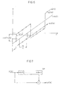
- Figure 1 shows an example of a temporal section of a determined by a measuring device Measurement signal (m (t)).
- Measuring devices such as sensors, bridge circuits or the like, which are used to measure such signals often have the disadvantage that they are Measurement signal m (t), which is of interest to the user, overlay a first offset signal, this is due to the mechanical sensitivity of the measuring arrangement, inaccuracies in the manufacturing technology of the measuring devices and / or through the electronics.
- Some sensors, such as Hall sensors or resistance bridges used for measuring purposes can be controlled so that the substantially constant first offset signal alternately added to the measurement signal m (t) in time with a first frequency f1 or is subtracted from this.
- Such a control of the measuring device can be done with Hall sensors for example by alternating current feed into the sensor at different Entrances are made.
- a first sum signal is present at the output of measuring devices controlled in this way s1 (t), which results from the sum of the measurement signal m (t) and a square wave signal the amplitude ot1 of the first offset and the first frequency f1.
- the first frequency f1 which is also referred to as the chopper frequency of the measuring device, is greater than the maximum frequency of the measurement signal m (t). Ideally differentiate the frequency of the measurement signal m (t) and the first frequency f1 of the offset signal a factor of 10 or more.
- the first frequency f1 and the second frequency f2 differ by a factor of eight.
- the first sum signal s1 (t) is sampled eight times during a period T1 of the offset signal.
- the sample values obtained by sampling with the sampling period T2 are represented by circles in FIG.
- the method further provides for the mean value to be formed from at least two of the sample values a1 (k) which were obtained at intervals of half a period T1 / 2 or odd multiples of half the period T1 / 2 of the offset signal.
- W1 (k) in FIG. 1 denotes a sequence of mean values which have been obtained by averaging two samples a1 (k) at intervals of half a period T1 / 2.
- the minimum period of the measurement signal m (t) is significantly larger than the half period T1 / 2 by which the samples a1 (k), a1 (k-n) to form the Mean values are spaced in time, and that the slope of the measurement signal m (t) in this Period T1 / 2 can therefore be assumed to be approximately constant the error resulting from the averaging on the actual measured value of the measurement signal m (t) can be neglected.
- the measurement signal m (t) or when the sequence of the measurement values w1 (k), of which - taking into account the time shift inserted by averaging - the measurement signal m (t) can be deduced goes through zero. Point of time the zero crossing is limited by the two measured values of the measured value sequence w (k), between which there has been a change of sign.
- the maximum temporal Uncertainty is 1 / T2 and decreases with increasing sampling frequency f2.
- FIG. 2 schematically shows a device according to the invention for carrying out the invention Process for the preparation of a measurement signal m (t) shown.
- the device has a measuring device S, with an output terminal on which a first Sum signal s1 (t) is available, which results from the superimposition of a measurement signal m (t) and an at least approximately rectangular offset signal with a first Frequency f1 and an amplitude ot1.
- the sensor is a clock signal TS first frequency f1 supplied, according to the measurement arrangement S "chopped" to the measurement signal m (t) an offset signal of the first frequency f1 instead of a DC signal to overlay.
- At an output of the scanning device AV lie in the the sampling values a1 (k) of the sum signal given by the sampling time pulse T2 s1 (t).
- the sequence of the samples a1 (k) is fed to a device MW for averaging, in that of two samples a1 (k), a1 (k-n), which are obtained by sampling at intervals half a period T1 / 2 of the offset signal or at intervals of an odd number Multiples of half the period T1 / 2 of the offset signal were obtained, the mean is formed.
- the amplitude of the sum signal s1 (t) is too small to be processed further by scanning to be able to.
- An amplifier V is therefore preferably connected downstream of the measuring arrangement, as shown in Figure 3.
- a second one Sum signal s2 (t) is formed in the scanning device AV with the clock period T2 .
- the sequence a2 (k) is the device MW to provide a sequence of measured values w2 (k) by forming the mean two samples a2 (k), a2 (k-n) are supplied.
- the amplification of the sum signal s1 (t) by means of conventional amplifiers, such as operational amplifiers has the disadvantage that the sum signal s1 (t) is inevitably a second Offset is added by the amplifier.
- the amplifier has an amplification element OP, for example an operational amplifier, which amplifies a signal s11 (t) added to it by a factor v and the amplified one Signal adds a second offset ot2.
- the reinforcing member OP is a first Upstream multiplier arrangement MUL1, the input signal of the amplifier V, in the first sum signal s1 (t) is supplied to the example, this signal s1 (t) after Provided a clock signal TS2 is multiplied by the factor "+1" or "-1" by the Rotate phase of the signal by 180 ° in accordance with the clock signal TS2.
- the phase shift of the input signal s1 (t) is connected downstream of the amplification element OP second multiplier arrangement MUL2 undone in which the output signal s21 (t) of the gain element OP in accordance with the clock signal TS2 with the factor "+1" or "-1" is multiplied.
- the multiplier arrangements MUL1, MUL2 have an im Clock of the clock signal TS2 switchable switch to an input of a multiplier alternately applies the value "+1" or "-1", whereby at a second input of the Multiplier the signal to be multiplied s11 (t); s21 (t) is present.
- the switching of the switches or the phase shift of the input signal s1 (t) and of the output signal s21 (t) is preferably carried out in time with the first frequency f1 or in Clock even multiple of the first frequency.
- FIG. 5 The functioning of the amplifier V is shown in FIG. 5 on the basis of selected signal profiles shown.
- Figure 1a shows an example of the waveform of an input signal s1 (t) of Amplifier V.
- At the output of the first multiplier MUL1 is one shown in FIG. 5b
- Signal s11 (t) which in sections due to the multiplication by "1” with the Input signal s1 (t) matches and in the other sections due to the multiplication is mirrored with "-1" on the time axis to the input signal s1 (t).
- the reinforcing member OP amplifies the signal s11 (t) present at its input with an amplification factor v and adds an offset of an amplitude ot2 to it, from which this is shown in FIG drawn signal s21 (t) results. For reasons of clarity, it was used as a gain factor v selected one in the example according to FIG. 5. Usual values for gain factors lie above 100. A signal amplified in this way would be corresponding in FIG. 5b moved up.
- the input signal s1 (t) of the amplifier v is an output signal of the measuring device S chosen in which a measurement signal m (t) by chopping the measurement arrangement S is an offset signal is superimposed on the first frequency f1, and the phase rotation of the signal s1 (t) takes place or S21 (t) in time with the first frequency f1 and in phase with the first offset signal, then is the output signal s2 (t) of the amplifier V, the amplified measurement signal v ⁇ m (t), the one Offset signal of the frequency f1 and the amplitude v ⁇ ot1 + ot2 is superimposed, as shown in FIG is.
- the further processing of this signal s2 (t) corresponds to that of the unamplified signal s1 (t), which was explained with reference to Figures 1 and 2.
- the signal s2 (t) is the second of the clock Frequency f2 sampled to provide a sequence of samples s2 (k).
- the education of the mean value from two samples each half a period apart T1 / 2 of the offset signal obtained by the scanning results in a sequence of measured values w2 (k) in time with the sampling frequency f2, which correspond to measured values of the measurement signal m (t), which are amplified by a factor of v, the values w2 (k) being approximately temporally opposite by T1 / 4 the actual measured values are shifted.
- the amplifier is chopped with a third frequency, which is an even multiple of the first frequency is f1, is obtained by the subsequent sampling and averaging the second offset ot2 inserted by the gain element OP is also eliminated.
- the amplifier does not have to be chopped in phase with the first offset signal.
- Amplification elements such as operational amplifiers, often have an inverting and one non-inverting input and one inverting and one non-inverting Exit on.
- the amplifier can be chopped by that the input signal alternately to the inverting in accordance with a clock signal and non-inverting input is applied and that the output signal in accordance with the same clock signal alternately on the inverting and non-inverting Output is tapped.
- the device has a storage device SP, preferably a shift register, in which a number Samples of the sequence of samples a1 (k), a2 (k) can be stored.
- the number of the memory cells preferably corresponds to the number n of samples in the time interval T1 / 2 are generated, which lies between the samples a1 (k), a1 (k-n); a2 (k), a2 (k-n) lies, which are used for averaging.
- the device also has an adder that holds the current sample a1 (k); a2 (k) and the previously created one Sample a1 (k-n); a2 (k-n) added.
- the output signal of the adder is multiplied by the factor 1/2 for correct averaging. Since often one anyway If the amplification of the measured values is desired, this multiplication by 1/2 can also be omitted become.
Landscapes
- Physics & Mathematics (AREA)
- General Physics & Mathematics (AREA)
- Measurement Of Current Or Voltage (AREA)
- Amplifiers (AREA)
- Measuring Frequencies, Analyzing Spectra (AREA)
Abstract
Description
- Figur 1:
- beispielhafter zeitlicher Verlauf eines Meßsignals, eines Summensignals aus Meßsignal und erstem Offsetsignal und einer gemäß dem erfindungsgemäßen Verfahren erzeugten Folge von Meßwerten;
- Figur 2:
- erfindungsgemäße Vorrichtung zur Durchführung des erfindungsgemäßen Verfahrens zur Aufbereitung eines Meßsignals;
- Figur 3:
- erfindungsgemäße Vorrichtung mit Verstärker;
- Figur 4:
- schematische Darstellung einer Ausführungsform des Verstärkers;
- Figur 5:
- beispielhafter zeitlicher Verlauf der Ein- und Ausgangssignale eines Verstärkers nach Figur 4;
- Figur 6:
- beispielhafter zeitlicher Verlauf eines Meßsignals, eines Summensignals aus Meßsignal und erstem Offsetsignal, eines Verstärkerausgangssignals und einer gemäß dem erfindungsgemäßen Verfahren erzeugten Folge von Meßwerten.
Claims (12)
- Verfahren zur Aufbereitung eines Meßsignals (m(t)), dem ein erstes Offsetsignal einer ersten Frequenz (f1) überlagert ist, wobei das Verfahren folgende Verfahrensschritte aufweist:Abtasten eines von der Summe aus dem Meßsignal m(t) und dem ersten Offsetsignal abhängigen Summensignals (s1(t); s2(t)) im Takt einer zweiten Frequenz (f2), die ein Vielfaches der ersten Frequenz (f1) ist, zur Bereitstellung einer Folge von Abtastwerten (a1(k); a2(k));Bereitstellen von Meßwerten (w1(k); w2(k)) des Meßsignals (m(t)) durch Addition oder Bildung des Mittelwertes von wenigstens zwei Abtastwerten (a1(k), a1(k-n); a2(k), a2(k-n)).
- Verfahren nach Anspruch 1,
dadurch gekennzeichnet, dass ein erstes Summensignal (s1(t)) aus dem Meßsignal (m(t)) und dem ersten Offsetsignal vor der Abtastung zur Bereitstellung eines zweiten Summensignals (s2(t)) verstärkt wird. - Verfahren nach Anspruch 1 oder 2,
dadurch gekennzeichnet, dass zur Bildung des Mittelwertes jeweils zwei Abtastwerte (a1(k), a(k-n); a2(k), a2(k-n)) addiert werden, die im zeitlichen Abstand der halben Periodendauer (T1/2) oder ungeradzahliger Vielfacher der halben Periodendauer (T1/2) des Offsetsignals gewonnen werden. - Verfahren nach einem der vorangehenden Ansprüche,
dadurch gekennzeichnet, dass die Verstärkung des ersten Summensignals (s1(t)) folgende Verfahrensschritte aufweist:Drehen der Phase des ersten Summensignals (s1(t)) in periodischen, durch eine dritte Frequenz vorgegebenen Zeitabständen um 180° zur Bereitstellung eines Signals s11(t);Verstärken des Signals s11(t) um einen Verstärkungsfaktor (v) zur Bereitstellung eines verstärkten Signals (s21(t));Drehen der Phase des verstärkten Signals (s21(t)) in periodischen, durch die dritte Frequenz vorgegebenen Zeitabständen um 180°. - Verfahren nach Anspruch 4,
dadurch gekennzeichnet, dass die dritte Frequenz gleich der ersten Frequenz oder ein geradzahliges Vielfaches der ersten Frequenz (f1) ist. - Verfahren nach Anspruch 4 oder 5,
dadurch gekennzeichnet, dass die Phasendrehung des ersten Summensignals (s1(t)) in Phase zu dem ersten Offsetsignal erfolgt. - Verfahren nach einem der vorangehenden Ansprüche,
dadurch gekennzeichnet, dass die Verstärkung des Summensignals (s2(t)) abhängig von der Amplitude des Meßsignals (m(t)) erfolgt. - Vorrichtung zur Aufbereitung eines Meßsignals (m(t)), dem ein Offsetsignal einer ersten Frequenz (f1) überlagert ist, wobei die Vorrichtung folgende Merkmale aufweist:eine Abtastvorrichtung (AV) zur Abtastung eines von der Summe des Meßsignals (m(t)) und des Offsetsignals abhängigen Summensignals (s1(t); s2(t)) im Takt einer zweiten Frequenz (f2) und zur Bereitstellung einer Folge von Abtastsignalen (a1(k); a2(k));eine der Abtastvorrichtung (AV) nachgeschaltete Vorrichtung zur (MW) Mittelwertbildung, der die Folge der Abtastwerte (a1(k); a2(k)) zugeführt ist, zur Bereitstellung von Meßwerten (w1(k); w2(k)) des Meßsignals (m(t)) durch Addition oder durch Bildung des Mittelwertes von wenigstens zwei Abtastwerten (a1(k), a1(k-n); a2(k), a2(k-n)).
- Vorrichtung nach Anspruch 8,
dadurch gekennzeichnet, dass der Abtastvorrichtung (AV) ein Verstärker (V) zur Bereitstellung eines zweiten Summensignals (s2(t)) durch Verstärkung eines ersten Summensignals (s1(t)) aus dem Meßsignal (m(t)) und dem Offsetsignal vorgeschaltet ist. - Vorrichtung nach Anspruch 9,
dadurch gekennzeichnet, dass der Verstärker (V) folgende Merkmale aufweist:eine erste Multiplizieranordnung (MUL1) zur Multiplikation eines Verstärkereingangssignals (s1(t)) mit einem Faktor "-1" im Takt einer dritten Frequenz (f3) und zur Bereitstellung eines Multiplikationssignals (s11(t));ein Verstärkungsglied (OP) zur Verstärkung des Multiplikationssignals (s11(t));eine zweite Multiplizieranordnung (MUL1) zur Multiplikation eines Ausgangssignals (s21(t)) des Verstärkungsglieds (OP) mit einem Faktor "-1" im Takt der dritten Frequenz (f3). - Vorrichtung nach einem der Ansprüche 8 bis 10,
dadurch gekennzeichnet, dass die Vorrichtung (MW) zur Mittelwertbildung einen Speicher (SP) zur Abspeicherung von Abtastwerten (a1(k-1),...,a1(k-n); a2(k-1),...,a2(k-n)) und einen Addierer (ADD) zur Addition eines abgespeicherten Abtastwertes (a1(k-n); a2(k-n)) und eines am Ausgang der Abtastvorrichtung (AV) anliegenden Abtastwertes (a1(k); a2(k)) aufweist. - Vorrichtung nach einem der Ansprüche 8 bis 11,
dadurch gekennzeichnet, dass in dem Speicher (SP) so viele Abtastwerte (a1(k-1),...,a1(k-n); a2(k-1),...,a2(k-n)) abspeicherbar sind, wie in einer halben Periodendauer (T1/2) des Offsetsignals durch Abtastung erzeugt werden.
Applications Claiming Priority (2)
| Application Number | Priority Date | Filing Date | Title |
|---|---|---|---|
| DE19946626 | 1999-09-29 | ||
| DE19946626A DE19946626A1 (de) | 1999-09-29 | 1999-09-29 | Verfahren und Vorrichtung zur Aufbereitung eines Messsignales |
Publications (3)
| Publication Number | Publication Date |
|---|---|
| EP1091214A2 true EP1091214A2 (de) | 2001-04-11 |
| EP1091214A3 EP1091214A3 (de) | 2004-05-19 |
| EP1091214B1 EP1091214B1 (de) | 2007-03-21 |
Family
ID=7923696
Family Applications (1)
| Application Number | Title | Priority Date | Filing Date |
|---|---|---|---|
| EP00119252A Expired - Lifetime EP1091214B1 (de) | 1999-09-29 | 2000-09-06 | Verfahren und Vorrichtung zur Aufbereitung von Messsignalen |
Country Status (3)
| Country | Link |
|---|---|
| US (1) | US6320430B1 (de) |
| EP (1) | EP1091214B1 (de) |
| DE (2) | DE19946626A1 (de) |
Cited By (1)
| Publication number | Priority date | Publication date | Assignee | Title |
|---|---|---|---|---|
| WO2017080547A1 (de) * | 2015-11-11 | 2017-05-18 | Schaeffler Technologies AG & Co. KG | Verfahren zum bestimmen eines korrigierten drehgeschwindigkeitssignals so-wie elektromotoranordnung |
Families Citing this family (3)
| Publication number | Priority date | Publication date | Assignee | Title |
|---|---|---|---|---|
| DE10204427B4 (de) | 2002-02-04 | 2007-02-22 | Infineon Technologies Ag | Verfahren und Vorrichtung zur Kompensation dynamischer Fehlersignale eines Chopped-Hall-Sensors |
| DE10223767B4 (de) * | 2002-05-28 | 2004-10-21 | Infineon Technologies Ag | Schaltungsanordnung zum Verarbeiten eines Signals eines Sensors |
| US8363699B2 (en) | 2009-03-20 | 2013-01-29 | On-Ramp Wireless, Inc. | Random timing offset determination |
Family Cites Families (9)
| Publication number | Priority date | Publication date | Assignee | Title |
|---|---|---|---|---|
| DE3905735A1 (de) * | 1989-02-24 | 1990-08-30 | Pierburg Gmbh | Verfahren zum auswerten eines eingangssignals |
| DE4336813B4 (de) * | 1993-10-28 | 2006-01-26 | Robert Bosch Gmbh | Vorrichtung zur Lasterfassung bei einer Brennkraftmaschine |
| US5469166A (en) * | 1994-07-19 | 1995-11-21 | Regev; Zvi Y. | Method to generate a continuous periodic signal from a short sample of the signal |
| DE59510984D1 (de) * | 1994-09-05 | 2005-02-10 | Landis & Gyr Ag Zug | Anordnung zum Messen elektrischer Energie |
| US5610950A (en) * | 1994-10-31 | 1997-03-11 | Motorola, Inc. | Communication device with reduced sensitivity to in-channel interference |
| US5621319A (en) * | 1995-12-08 | 1997-04-15 | Allegro Microsystems, Inc. | Chopped hall sensor with synchronously chopped sample-and-hold circuit |
| US5847558A (en) * | 1996-07-10 | 1998-12-08 | Philips Electronics North America Corporation | Periodic signal analyzer using a randomly varied phase shifting circuit |
| DE19913753A1 (de) * | 1998-04-01 | 1999-10-07 | Mannesmann Rexroth Ag | Verfahren zur Bildung des Mittelwertes |
| US6049297A (en) * | 1998-11-19 | 2000-04-11 | Visidyne, Corp. | Digital phase measuring system and method |
-
1999
- 1999-09-29 DE DE19946626A patent/DE19946626A1/de not_active Ceased
-
2000
- 2000-09-06 DE DE50014178T patent/DE50014178D1/de not_active Expired - Lifetime
- 2000-09-06 EP EP00119252A patent/EP1091214B1/de not_active Expired - Lifetime
- 2000-09-29 US US09/675,794 patent/US6320430B1/en not_active Expired - Fee Related
Cited By (4)
| Publication number | Priority date | Publication date | Assignee | Title |
|---|---|---|---|---|
| WO2017080547A1 (de) * | 2015-11-11 | 2017-05-18 | Schaeffler Technologies AG & Co. KG | Verfahren zum bestimmen eines korrigierten drehgeschwindigkeitssignals so-wie elektromotoranordnung |
| CN108139427A (zh) * | 2015-11-11 | 2018-06-08 | 舍弗勒技术股份两合公司 | 用于确定经修正的转速信号的方法以及电动机装置 |
| US10209268B2 (en) | 2015-11-11 | 2019-02-19 | Schaeffler Technologies AG & Co. KG | Method for determining a corrected rotational speed signal, and electric motor arrangement |
| CN108139427B (zh) * | 2015-11-11 | 2020-09-11 | 舍弗勒技术股份两合公司 | 用于确定经修正的转速信号的方法以及电动机装置 |
Also Published As
| Publication number | Publication date |
|---|---|
| DE50014178D1 (de) | 2007-05-03 |
| EP1091214A3 (de) | 2004-05-19 |
| DE19946626A1 (de) | 2001-04-26 |
| EP1091214B1 (de) | 2007-03-21 |
| US6320430B1 (en) | 2001-11-20 |
Similar Documents
| Publication | Publication Date | Title |
|---|---|---|
| EP0707383B1 (de) | Schaltungsanordnung zur Analog-Digital-Wandlung von Signalen | |
| DE19502047C2 (de) | Verfahren zur Analog-Digital-Wandlung von Signalen | |
| DE10223767B4 (de) | Schaltungsanordnung zum Verarbeiten eines Signals eines Sensors | |
| EP0141080B1 (de) | Auswerteschaltungen für passive Messgrössenaufnehmer | |
| DE102018201310B4 (de) | Stromsensor und Schutzschalter | |
| DE102008023535A1 (de) | Elektronische Vorrichtung und Verfahren zur Auswertung einer variablen Kapazität | |
| DE3135158A1 (de) | Zeitintervall-messanordnung | |
| DE2636063A1 (de) | Spitzenwertdetektor | |
| DE3642771A1 (de) | Verfahren und vorrichtung zur messung der messgroesse eines messobjekts | |
| EP2021812B1 (de) | Messvorrichtung mit gegengekoppeltem gleichspannungsverstärker | |
| DE69009619T2 (de) | Vorrichtung zur Messung vom Effektivwert eines Signales, insbesondere zur Messung des Stromes in einem statischen Auslöser. | |
| DE60029113T2 (de) | Störfeldfestes näherungssensorsystem mit einer impedanzauswertung durch nachführen einer resonanzfrequenz | |
| EP1091214B1 (de) | Verfahren und Vorrichtung zur Aufbereitung von Messsignalen | |
| DE3340330A1 (de) | Verfahren und anordnung zur kompensation eines sich zeitlich nichtlinear aendernden elektrischen signals | |
| EP1495295A2 (de) | Messverstärkervorrichtung | |
| EP0615669B1 (de) | Verfahren und schaltung zur messung von teilchenströmen | |
| DE102006017239A1 (de) | Differentieller Levelshifter mit automatischem Fehlerabgleich | |
| EP0942564B1 (de) | Verfahren zur Detektion eines gepulsten Nutzsignals | |
| EP0777130A2 (de) | Digitales Verfahren zur Detektion zeitlich kurzer Pulse und Anordnung zur Durchführung des Verfahrens | |
| DE69424931T2 (de) | Analog/Digital-Wandler für niederfrequente, differentielle Signale geringer Amplitude | |
| EP0412573B1 (de) | Schaltungsanordnung für die Analogsignal-Frequenz-Wandlung | |
| DE3143669C2 (de) | Schaltung zum Messen des Effektivwertes einer Wechselspannung | |
| DE10005605B4 (de) | Analoge Vorstufe | |
| DE102020130115A1 (de) | Messvorrichtung zur Vermessung des Busstromes in einer Datenbusleitung mit Zwischenspeicherung der Offsetspannung eines Differenzverstärkers mit fünf Schaltern | |
| DE2803639C3 (de) | Analog-Digital-VerschlüBter für passive Meßwertgeber mit Gleichstromspeisung |
Legal Events
| Date | Code | Title | Description |
|---|---|---|---|
| PUAI | Public reference made under article 153(3) epc to a published international application that has entered the european phase |
Free format text: ORIGINAL CODE: 0009012 |
|
| AK | Designated contracting states |
Kind code of ref document: A2 Designated state(s): AT BE CH CY DE DK ES FI FR GB GR IE IT LI LU MC NL PT SE |
|
| AX | Request for extension of the european patent |
Free format text: AL;LT;LV;MK;RO;SI |
|
| PUAL | Search report despatched |
Free format text: ORIGINAL CODE: 0009013 |
|
| AK | Designated contracting states |
Kind code of ref document: A3 Designated state(s): AT BE CH CY DE DK ES FI FR GB GR IE IT LI LU MC NL PT SE |
|
| AX | Request for extension of the european patent |
Extension state: AL LT LV MK RO SI |
|
| 17P | Request for examination filed |
Effective date: 20041009 |
|
| AKX | Designation fees paid |
Designated state(s): DE FR GB IT NL |
|
| 17Q | First examination report despatched |
Effective date: 20050502 |
|
| GRAP | Despatch of communication of intention to grant a patent |
Free format text: ORIGINAL CODE: EPIDOSNIGR1 |
|
| GRAS | Grant fee paid |
Free format text: ORIGINAL CODE: EPIDOSNIGR3 |
|
| GRAA | (expected) grant |
Free format text: ORIGINAL CODE: 0009210 |
|
| AK | Designated contracting states |
Kind code of ref document: B1 Designated state(s): DE FR GB IT NL |
|
| REG | Reference to a national code |
Ref country code: GB Ref legal event code: FG4D Free format text: NOT ENGLISH |
|
| GBT | Gb: translation of ep patent filed (gb section 77(6)(a)/1977) |
Effective date: 20070321 |
|
| REF | Corresponds to: |
Ref document number: 50014178 Country of ref document: DE Date of ref document: 20070503 Kind code of ref document: P |
|
| ET | Fr: translation filed | ||
| PLBE | No opposition filed within time limit |
Free format text: ORIGINAL CODE: 0009261 |
|
| STAA | Information on the status of an ep patent application or granted ep patent |
Free format text: STATUS: NO OPPOSITION FILED WITHIN TIME LIMIT |
|
| 26N | No opposition filed |
Effective date: 20071227 |
|
| PGFP | Annual fee paid to national office [announced via postgrant information from national office to epo] |
Ref country code: NL Payment date: 20090915 Year of fee payment: 10 |
|
| PGFP | Annual fee paid to national office [announced via postgrant information from national office to epo] |
Ref country code: IT Payment date: 20090924 Year of fee payment: 10 |
|
| REG | Reference to a national code |
Ref country code: NL Ref legal event code: V1 Effective date: 20110401 |
|
| PG25 | Lapsed in a contracting state [announced via postgrant information from national office to epo] |
Ref country code: IT Free format text: LAPSE BECAUSE OF NON-PAYMENT OF DUE FEES Effective date: 20100906 |
|
| PG25 | Lapsed in a contracting state [announced via postgrant information from national office to epo] |
Ref country code: NL Free format text: LAPSE BECAUSE OF NON-PAYMENT OF DUE FEES Effective date: 20110401 |
|
| PGFP | Annual fee paid to national office [announced via postgrant information from national office to epo] |
Ref country code: DE Payment date: 20130919 Year of fee payment: 14 |
|
| PGFP | Annual fee paid to national office [announced via postgrant information from national office to epo] |
Ref country code: FR Payment date: 20130919 Year of fee payment: 14 Ref country code: GB Payment date: 20130919 Year of fee payment: 14 |
|
| REG | Reference to a national code |
Ref country code: DE Ref legal event code: R119 Ref document number: 50014178 Country of ref document: DE |
|
| GBPC | Gb: european patent ceased through non-payment of renewal fee |
Effective date: 20140906 |
|
| REG | Reference to a national code |
Ref country code: DE Ref legal event code: R119 Ref document number: 50014178 Country of ref document: DE Effective date: 20150401 |
|
| REG | Reference to a national code |
Ref country code: FR Ref legal event code: ST Effective date: 20150529 |
|
| PG25 | Lapsed in a contracting state [announced via postgrant information from national office to epo] |
Ref country code: DE Free format text: LAPSE BECAUSE OF NON-PAYMENT OF DUE FEES Effective date: 20150401 Ref country code: GB Free format text: LAPSE BECAUSE OF NON-PAYMENT OF DUE FEES Effective date: 20140906 |
|
| PG25 | Lapsed in a contracting state [announced via postgrant information from national office to epo] |
Ref country code: FR Free format text: LAPSE BECAUSE OF NON-PAYMENT OF DUE FEES Effective date: 20140930 |