EP1089422A2 - Alimentation de puissance à découpage résonante - Google Patents
Alimentation de puissance à découpage résonante Download PDFInfo
- Publication number
- EP1089422A2 EP1089422A2 EP00117156A EP00117156A EP1089422A2 EP 1089422 A2 EP1089422 A2 EP 1089422A2 EP 00117156 A EP00117156 A EP 00117156A EP 00117156 A EP00117156 A EP 00117156A EP 1089422 A2 EP1089422 A2 EP 1089422A2
- Authority
- EP
- European Patent Office
- Prior art keywords
- resonant
- switching
- circuit
- power supply
- load
- Prior art date
- Legal status (The legal status is an assumption and is not a legal conclusion. Google has not performed a legal analysis and makes no representation as to the accuracy of the status listed.)
- Withdrawn
Links
Images


Classifications
-
- H—ELECTRICITY
- H02—GENERATION; CONVERSION OR DISTRIBUTION OF ELECTRIC POWER
- H02M—APPARATUS FOR CONVERSION BETWEEN AC AND AC, BETWEEN AC AND DC, OR BETWEEN DC AND DC, AND FOR USE WITH MAINS OR SIMILAR POWER SUPPLY SYSTEMS; CONVERSION OF DC OR AC INPUT POWER INTO SURGE OUTPUT POWER; CONTROL OR REGULATION THEREOF
- H02M3/00—Conversion of dc power input into dc power output
- H02M3/22—Conversion of dc power input into dc power output with intermediate conversion into ac
- H02M3/24—Conversion of dc power input into dc power output with intermediate conversion into ac by static converters
- H02M3/28—Conversion of dc power input into dc power output with intermediate conversion into ac by static converters using discharge tubes with control electrode or semiconductor devices with control electrode to produce the intermediate ac
- H02M3/325—Conversion of dc power input into dc power output with intermediate conversion into ac by static converters using discharge tubes with control electrode or semiconductor devices with control electrode to produce the intermediate ac using devices of a triode or a transistor type requiring continuous application of a control signal
- H02M3/335—Conversion of dc power input into dc power output with intermediate conversion into ac by static converters using discharge tubes with control electrode or semiconductor devices with control electrode to produce the intermediate ac using devices of a triode or a transistor type requiring continuous application of a control signal using semiconductor devices only
- H02M3/33569—Conversion of dc power input into dc power output with intermediate conversion into ac by static converters using discharge tubes with control electrode or semiconductor devices with control electrode to produce the intermediate ac using devices of a triode or a transistor type requiring continuous application of a control signal using semiconductor devices only having several active switching elements
- H02M3/33573—Full-bridge at primary side of an isolation transformer
-
- H—ELECTRICITY
- H02—GENERATION; CONVERSION OR DISTRIBUTION OF ELECTRIC POWER
- H02M—APPARATUS FOR CONVERSION BETWEEN AC AND AC, BETWEEN AC AND DC, OR BETWEEN DC AND DC, AND FOR USE WITH MAINS OR SIMILAR POWER SUPPLY SYSTEMS; CONVERSION OF DC OR AC INPUT POWER INTO SURGE OUTPUT POWER; CONTROL OR REGULATION THEREOF
- H02M3/00—Conversion of dc power input into dc power output
- H02M3/01—Resonant DC/DC converters
-
- H—ELECTRICITY
- H02—GENERATION; CONVERSION OR DISTRIBUTION OF ELECTRIC POWER
- H02M—APPARATUS FOR CONVERSION BETWEEN AC AND AC, BETWEEN AC AND DC, OR BETWEEN DC AND DC, AND FOR USE WITH MAINS OR SIMILAR POWER SUPPLY SYSTEMS; CONVERSION OF DC OR AC INPUT POWER INTO SURGE OUTPUT POWER; CONTROL OR REGULATION THEREOF
- H02M3/00—Conversion of dc power input into dc power output
- H02M3/22—Conversion of dc power input into dc power output with intermediate conversion into ac
- H02M3/24—Conversion of dc power input into dc power output with intermediate conversion into ac by static converters
- H02M3/28—Conversion of dc power input into dc power output with intermediate conversion into ac by static converters using discharge tubes with control electrode or semiconductor devices with control electrode to produce the intermediate ac
- H02M3/325—Conversion of dc power input into dc power output with intermediate conversion into ac by static converters using discharge tubes with control electrode or semiconductor devices with control electrode to produce the intermediate ac using devices of a triode or a transistor type requiring continuous application of a control signal
- H02M3/335—Conversion of dc power input into dc power output with intermediate conversion into ac by static converters using discharge tubes with control electrode or semiconductor devices with control electrode to produce the intermediate ac using devices of a triode or a transistor type requiring continuous application of a control signal using semiconductor devices only
- H02M3/33569—Conversion of dc power input into dc power output with intermediate conversion into ac by static converters using discharge tubes with control electrode or semiconductor devices with control electrode to produce the intermediate ac using devices of a triode or a transistor type requiring continuous application of a control signal using semiconductor devices only having several active switching elements
- H02M3/33571—Half-bridge at primary side of an isolation transformer
-
- Y—GENERAL TAGGING OF NEW TECHNOLOGICAL DEVELOPMENTS; GENERAL TAGGING OF CROSS-SECTIONAL TECHNOLOGIES SPANNING OVER SEVERAL SECTIONS OF THE IPC; TECHNICAL SUBJECTS COVERED BY FORMER USPC CROSS-REFERENCE ART COLLECTIONS [XRACs] AND DIGESTS
- Y02—TECHNOLOGIES OR APPLICATIONS FOR MITIGATION OR ADAPTATION AGAINST CLIMATE CHANGE
- Y02B—CLIMATE CHANGE MITIGATION TECHNOLOGIES RELATED TO BUILDINGS, e.g. HOUSING, HOUSE APPLIANCES OR RELATED END-USER APPLICATIONS
- Y02B70/00—Technologies for an efficient end-user side electric power management and consumption
- Y02B70/10—Technologies improving the efficiency by using switched-mode power supplies [SMPS], i.e. efficient power electronics conversion e.g. power factor correction or reduction of losses in power supplies or efficient standby modes
Definitions
- the present invention relates to a resonant switching power supply, more particularly, to a resonant switching power supply with zero voltage and zero current switch feature, whereby the power consumption is reduced and electromagnetic radiation is minimized.
- Figs. 1 and 2 show two type of conventional resonant switching power supplies. Those resonant switching power supplies use resonant circuit composed of inductor and capacitor to generate sinusoid wave, and the zero cross points of the sinusoid wave to provide zero-voltage switching (ZVS) or zero-current switching (ZCS).
- ZVS zero-voltage switching
- ZCS zero-current switching
- This technique can be roughly classified as serial load resonant (SLR) as shown in Fig. 1 and parallel load resonant (PLR) as shown in Fig. 2.
- SLR serial load resonant
- PLR parallel load resonant
- the frequency of the input voltage is designed to be the same as the resonant frequency as the resonant circuit to provide most efficient output.
- the optimal operation relies on the assumption of constant load, this is rare in practical situation.
- Another conventional resonant switching power supply which is a full bridge ZVS PWM converter.
- the full bridge ZVS PWM converter uses four sets of switches. Therefore, the circuit is complicated and the parasitic capacitance and leak inductance is hard to manipulate, thus being difficult to mass production.
- this full bridge ZVS PWM converter is not economic in light load application, especially hard to ensure zero-voltage switching (ZVS) or zero-current switching (ZCS) in a light load application,
- the present invention is intended to provide a resonant switching power supply with zero voltage and zero current switch feature, which can be operated in a half-bridge or a full-bridge scheme.
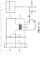
- Fig. 3a shows the circuit diagram of a resonant switching power supply according to a first preferred embodiment of the present invention. It should be noted that the circuit shown in Fig. 3a is a half-bridge switching power supply, however, the principle of the present invention can also be applied to the full-bridge switching power supply as shown in Fig. 3b.
- the symbols SW1 and SW2 denote switching elements and can be implemented by FET, transistor or IGBT.
- the symbols C1 and C2 denote the parasitic capacitance of the switching elements SW1 and SW2, respectively.
- D1 and D2 are by-pass diodes
- C3 resonant capacitor
- C4 and C5 by-pass capacitors for power supply
- L1 resonant inductor
- T1 transformer
- D3 and D4 output rectifying diode
- L2 flywheel inductor for storing and removing energy
- C6 output filtering capacitor and parallel with load to smooth the output voltage.
- the resonant switching power supply according to the first preferred embodiment of the present invention further comprises a feedback control circuit F, which can detect the load condition and generate a control pulse to control the operation of the first switch SW1 and the second switch SW2.
- Fig. 5a shows a simplified circuit of the circuit shown in Fig. 3a.
- Fig. 5b shows the waveforms of switch driving voltage and resonant current in circuit of Fig. 3a.
- Fig. 6 shows the voltage or current waveforms of several elements or nodes in circuit of Fig. 3a.
- Fig. 7 also shows the voltage or current waveforms of several elements or nodes in circuit of Fig. 3a.
- the first switch SW1 and the second switch SW2 have timing diagram as shown in curve 1 and 2 in Fig. 6.
- the theoretical value of voltage between the nodes A and C in Fig. 3a is shown in curve 3 of Fig. 6.
- the resonant current is shown in curve 4 of Fig. 6.
- the first switch SW1 and the second switch SW2 are square waves with duty ratio smaller than 50%. It will be explained below that the choice of duty ratio, in conjunction with the particular choice of switch driving frequency, will induce the effect of zero voltage and zero current switch. More particularly, in the resonant switching power supply shown in Fig.
- the frequencies of the driving pulses for the first switch SW1 and the second switch SW2 are selected to slightly deviate from the resonant frequency of the resonant frequency ⁇ 0 decided by the resonant inductor L1 and the resonant capacitor C3, and the driving pulses are continuously generated as shown in the curves 1 and 2.
- the voltage between nodes A and C slightly leads the resonant current (curve 4).
- the resonant switching power supply according to the present invention uses switching signal with duty ratio smaller than 50% and particular selected frequency of the switching signal to induce advantageous interaction between the remaining current in the resonant circuit and the parasitic capacitance C1 and C2 of the switching elements SW1 and SW2, thus achieving zero voltage and zero current switch. This will be explained in more detail below.
- Fig. 5a is the simplified circuit of that in Fig. 3a and Fig. 5b shows the voltage between nodes A and C (square wave) induced by the switching signal and the resonant current (sinusoid wave).
- the resonant current I Ll is positive
- switch SW 1 is shorted circuit
- switch SW 2 is open circuit.
- the voltage at node A is Vcc
- the voltage across the capacitor C1 is zero
- the voltage across the capacitor C2 is 2Vcc.
- the diodes D1 and D2 are reverse bias and conduct no current.
- the current I Ll decreases gradually.
- the current I Ll is near zero and the SW 1 becomes open circuit. Because the current in the inductor L1 should be continuous, a certain amount of positive current still flows into the resonant circuit. At this time, the switch SW 1 is nearly zero current switching. Moreover, the voltage of the switch SW 1 is established by charging the parasitic capacitance C1 thereof with the infinitesimal resonant current, thus achieving zero voltage switch. As time goes by, the capacitor C1 is charged and the capacitor C2 is discharged. The voltage at node A changes from +Vcc to -Vcc rapidly and the voltage of SW2 is dropped from 2Vcc to 0.
- the operation principle of the resonant switching power supply is similar to previously described.
- the switch SW1 replaces the role of switch SW2, C1 replaces C2, D1 replaces D2, and vice versa.
- the resonant switching power supply still has high efficiency and the diodes D1 and D2 have infinitesimal current flowing therethrough if the phase of the switch driving signal leads the phase of the resonant current.
- a phase control circuit (not shown) can be incorporated into the resonant switching power supply to stabilize the frequency of the switching driving signal. Therefore, the switching time will not have error.
- the resonant switching power supply in the present invention is not sensitive to the value of parasitic capacitance and leak inductance, which hinders the conventional full bridge ZVS PWM converter.
- the conventional full bridge ZVS PWM converters while switch at zero voltage, have considerable switching current. Therefore, the parasitic capacitance has rapid charging time and the discharging time of the leak inductance should be well controlled, or the performance of the conventional full bridge ZVS PWM converter is degraded.
- the resonant switching power supply in the present invention is operated in a zero voltage and zero current switch manner. The influence of parasitic capacitance and leak inductance is minimized.
- a feedback control circuit F is incorporated into the resonant switching power supply in the present invention.
- the feedback control circuit F detects the load condition and generates a lower frequency control pulse to control the operation of the switch driving signals for the first switch SW1 and the second switch SW2. More particularly, the switch driving signals for the first switch SW1 and the second switch SW2 generally have relatively high frequency such as 100KHz.
- the feedback control circuit F generates a control pulse with lower frequency, e.g. 1KHz (as shown in the curve 6 in Fig. 7) to modulate the switch driving signals for SW1 and SW2 in response to the load condition. Therefore, the switch driving signals for the first switch SW1 and the second switch SW2 become intermittent rather than continuous.
- the switch driving signals for the first switch SW1 and the second switch SW2 are enabled when the control pulse (curve 6) is high, and disabled when the control pulse is low. Moreover, if the control signal is not carefully applied, the control signal will truncate the switch driving signals as indicated by the time period t5-t6. As a result, noise will be generated (as shown in the curve 10 of Fig. 7) and the efficiency of the inventive resonant switching power supply is degraded. Therefore, the control pulse according to the present invention should cover switch driving signals of integer number and does truncates the switch driving signals as indicated by the time period t5'-t6'. The resonant switching power supply generates noise-free resonant current as indicated by curve 9 of Fig. 7. The effeteness of the feedback control circuit is also experimentally validated.
- the inventive resonant switching power supply is designed to have special output circuit.
- the conventional output circuit shown in Fig. 8a (for full-wave rectification circuit, the output circuit for half-wave rectification is shown in Fig. 8b) has two problems. Firstly, the diodes D3 and D4 conduct instantaneously when the output voltage of the transformer T1 exceeds the voltage Vc of the capacitor C6. The transformer T1 "see” a low output impedance instantaneously and large amount of current flows through the diodes D3 and D4. As a result, the waveform of the resonant current and resonant voltage is distorted and unwanted high-frequency noise is generated as shown in the curve 10 of the Fig. 7.
- the diodes D3 and D4 are open circuit instantaneously when the output voltage of the transformer T1 is below the voltage Vc of the capacitor C6. .
- the transformer T1 "see” a high output impedance instantaneously, and the resonant circuit has a high Q value.
- the remaining current will keep oscillating within the high-Q resonant circuit such that energy is dissipated in the resonant circuit and can not output, as shown in the curve 9 of Fig. 7.
- the efficiency of the switching power supply is degraded, thermal energy is generated and the remaining oscillation may encounter the next switch driving pulse to generate noise.
- a flywheel inductor L2 for storing and removing energy is incorporated in the output circuit as shown in Fig. 10a (for full- wave rectification circuit, the output circuit for half-wave rectification is shown in Fig. 10b).
- Fig. 10a for full- wave rectification circuit, the output circuit for half-wave rectification is shown in Fig. 10b.
- the inductor used in the forward switching power supply as shown in Fig. 9a (for full- wave rectification circuit, the output circuit for half-bridge is shown in Fig. 9b)
- the inductor is used to isolate the output end of the transformer with the capacitor and a flywheel diode is required to remove the flywheel current of the inductor forward current.
- Fig. 4a shows the circuit diagram of a resonant switching power supply according to second preferred embodiment of the present invention. It should be noted that the circuit shown in Fig. 4a is a half-bridge switching power supply, however, the principle of the present invention can also be applied to the full-bridge switching power supply as shown in Fig. 4b.
- the resonant switching power supply shown in Fig. 4a is similar to that shown in Fig. 3a except that the transformer T1 replaces the function of the resonant inductor L1, i.e., the resonant inductor L1 is eliminated to save cost.
- switching signal has duty ratio smaller than 50% to induce advantageous interaction between the remaining current in the resonant circuit and the parasitic capacitance C1 and C2 of the switching elements SW1 and SW2, thus achieving zero voltage and zero current switch.
- the present invention provides a resonant switching power supply with high efficiency and low electromagnetic radiation.
- the inventive resonant switching power supply is insensitive to the parasitic capacitance and leak inductance, thus eliminating complicated calibration process.
- the feedback control circuit can be easily implemented by simple digital circuit to reduce noise due to fluctuant load.
- the zero voltage and zero current switch feature can be realized by engineer the operation frequency of the switch driving signal to deviate form the resonant frequency such that the phase of the switch driving signal leads the resonant current.
- the inventive resonant switching power supply has simple circuit and can be easily adapted to use in half-bridge circuit or full-bridge circuit.
Applications Claiming Priority (2)
| Application Number | Priority Date | Filing Date | Title |
|---|---|---|---|
| US408722 | 1999-09-29 | ||
| US09/408,722 US6147881A (en) | 1999-09-29 | 1999-09-29 | Resonant switching power supply |
Publications (1)
| Publication Number | Publication Date |
|---|---|
| EP1089422A2 true EP1089422A2 (fr) | 2001-04-04 |
Family
ID=23617483
Family Applications (1)
| Application Number | Title | Priority Date | Filing Date |
|---|---|---|---|
| EP00117156A Withdrawn EP1089422A2 (fr) | 1999-09-29 | 2000-08-10 | Alimentation de puissance à découpage résonante |
Country Status (2)
| Country | Link |
|---|---|
| US (1) | US6147881A (fr) |
| EP (1) | EP1089422A2 (fr) |
Cited By (2)
| Publication number | Priority date | Publication date | Assignee | Title |
|---|---|---|---|---|
| EP1501177A2 (fr) * | 2003-07-24 | 2005-01-26 | Harman International Industries, Incorporated | Alimentation de puissance avec correction du facteur de puissance |
| US7403400B2 (en) | 2003-07-24 | 2008-07-22 | Harman International Industries, Incorporated | Series interleaved boost converter power factor correcting power supply |
Families Citing this family (16)
| Publication number | Priority date | Publication date | Assignee | Title |
|---|---|---|---|---|
| US6807073B1 (en) | 2001-05-02 | 2004-10-19 | Oltronics, Inc. | Switching type power converter circuit and method for use therein |
| AU2002359832A1 (en) * | 2001-12-31 | 2003-07-24 | Bae Systems Information And Electronic Systems Integration, Inc. | Logic controlled high voltage resonant switching power supply |
| US6930893B2 (en) * | 2002-01-31 | 2005-08-16 | Vlt, Inc. | Factorized power architecture with point of load sine amplitude converters |
| US6975098B2 (en) * | 2002-01-31 | 2005-12-13 | Vlt, Inc. | Factorized power architecture with point of load sine amplitude converters |
| CN1316724C (zh) * | 2003-07-03 | 2007-05-16 | 南京航空航天大学 | 电流控制型半桥变换器的分压电容电压偏差前馈控制电路 |
| JP4534223B2 (ja) * | 2004-04-30 | 2010-09-01 | ミネベア株式会社 | Dc−dcコンバータ |
| US20060227584A1 (en) * | 2005-04-12 | 2006-10-12 | Kan-Sheng Kuan | Zero-voltage-switching electric converter |
| US7375994B2 (en) * | 2005-10-11 | 2008-05-20 | Texas Instruments Incorporated | Highly efficient isolated AC/DC power conversion technique |
| KR20070087850A (ko) * | 2005-12-29 | 2007-08-29 | 이광직 | 증폭된 공진전력을 부하에 전달하는 회로 |
| US8725245B2 (en) * | 2006-08-14 | 2014-05-13 | Kimberly-Clark Worldwide, Inc. | Resonant coil for measuring specimen condition |
| WO2010055568A1 (fr) * | 2008-11-13 | 2010-05-20 | 株式会社MERSTech | Interrupteur à régénération d’énergie magnétique pourvu d’un circuit de protection |
| US8384378B2 (en) * | 2009-02-27 | 2013-02-26 | Kimberly-Clark Worldwide, Inc. | Conductivity sensor |
| US8452388B2 (en) * | 2009-02-27 | 2013-05-28 | Kimberly-Clark Worldwide, Inc. | Apparatus and method for assessing vascular health |
| CN101771360B (zh) * | 2010-03-05 | 2012-03-14 | 北京嘉昌机电设备制造有限公司 | 一种开关电源中动态磁平衡调整电路及开关电源 |
| TWI452809B (zh) * | 2011-03-08 | 2014-09-11 | Green Solution Tech Co Ltd | 全橋驅動控制電路及全橋式轉換電路 |
| US10020752B1 (en) * | 2017-09-26 | 2018-07-10 | Vlt, Inc. | Adaptive control of resonant power converters |
Family Cites Families (9)
| Publication number | Priority date | Publication date | Assignee | Title |
|---|---|---|---|---|
| JP3199423B2 (ja) * | 1991-11-01 | 2001-08-20 | オリジン電気株式会社 | 共振形フォワードコンバ−タ |
| US5327337A (en) * | 1992-09-01 | 1994-07-05 | Broadcast Electronics, Inc. | Resonant push-pull switching power amplifier |
| KR100219314B1 (ko) * | 1992-09-25 | 1999-09-01 | 무라따 미치히로 | 공진형 전원 회로 |
| DE19529941A1 (de) * | 1995-08-16 | 1997-02-20 | Philips Patentverwaltung | Spannungskonverter |
| US5646835A (en) * | 1995-11-20 | 1997-07-08 | General Electric Company | Series resonant converter |
| KR100199506B1 (ko) * | 1996-10-29 | 1999-06-15 | 윤문수 | 출력전류의 리플 저감이 가능한 풀 브릿지 디씨이/디씨이컨버터의 영전압/영전류 스위칭을 위한 회로 |
| US5808879A (en) * | 1996-12-26 | 1998-09-15 | Philips Electronics North America Corporatin | Half-bridge zero-voltage-switched PWM flyback DC/DC converter |
| US5774346A (en) * | 1997-01-24 | 1998-06-30 | Poon; Franki Ngai Kit | Family of zero voltage switching DC to DC converters with coupled output inductor |
| US5768112A (en) * | 1997-05-30 | 1998-06-16 | Delco Electronics Corp. | Sub-resonant series resonant converter having improved form factor and reduced EMI |
-
1999
- 1999-09-29 US US09/408,722 patent/US6147881A/en not_active Expired - Fee Related
-
2000
- 2000-08-10 EP EP00117156A patent/EP1089422A2/fr not_active Withdrawn
Cited By (3)
| Publication number | Priority date | Publication date | Assignee | Title |
|---|---|---|---|---|
| EP1501177A2 (fr) * | 2003-07-24 | 2005-01-26 | Harman International Industries, Incorporated | Alimentation de puissance avec correction du facteur de puissance |
| EP1501177A3 (fr) * | 2003-07-24 | 2006-04-19 | Harman International Industries, Incorporated | Alimentation de puissance avec correction du facteur de puissance |
| US7403400B2 (en) | 2003-07-24 | 2008-07-22 | Harman International Industries, Incorporated | Series interleaved boost converter power factor correcting power supply |
Also Published As
| Publication number | Publication date |
|---|---|
| US6147881A (en) | 2000-11-14 |
Similar Documents
| Publication | Publication Date | Title |
|---|---|---|
| US6147881A (en) | Resonant switching power supply | |
| Lee | High-frequency quasi-resonant converter technologies | |
| US5159541A (en) | Asymmetrical pulse width modulated resonant DC/DC converter | |
| US5140510A (en) | Constant frequency power converter | |
| US5438498A (en) | Series resonant converter having a resonant snubber | |
| US7924578B2 (en) | Two terminals quasi resonant tank circuit | |
| US5986895A (en) | Adaptive pulse width modulated resonant Class-D converter | |
| JP3326754B2 (ja) | 定周波共振型dc/dcコンバータ | |
| US4785387A (en) | Resonant converters with secondary-side resonance | |
| US6442047B1 (en) | Power conversion apparatus and methods with reduced current and voltage switching | |
| EP0503862B1 (fr) | Convertisseur de classe E à fréquence fixe | |
| JP2011526478A (ja) | 共振型電力コンバータ | |
| WO2000048300A1 (fr) | Convertisseur indirect de commutation sur une tension nulle d'une resonance decalee | |
| US6097614A (en) | Asymmetrical pulse width modulated resonant DC-DC converter with compensating circuitry | |
| US5644479A (en) | Switching power supply device | |
| TWI791594B (zh) | 共振功率轉換器 | |
| JP2001157448A (ja) | 共振スイッチング電源装置 | |
| US6590786B2 (en) | System for controlling the delivery of power to DC computer components utilizing phase shift regulation | |
| EP3447890B1 (fr) | Convertisseur résonant modulé de ligne reconfigurable | |
| Ray | Bidirectional DC/DC power conversion using quasi-resonant topology | |
| CN111525803B (zh) | 变换装置 | |
| JPH05207740A (ja) | Dc−dcコンバ−タ回路 | |
| US6621718B1 (en) | Resonant converter circuit | |
| Birca-Galateanu et al. | Class E low dv/dt and low di/dt rectifiers: energy transfer, comparison, compact relationships | |
| KR20020012885A (ko) | 공진 스위칭 파워 서플라이 |
Legal Events
| Date | Code | Title | Description |
|---|---|---|---|
| PUAI | Public reference made under article 153(3) epc to a published international application that has entered the european phase |
Free format text: ORIGINAL CODE: 0009012 |
|
| AK | Designated contracting states |
Kind code of ref document: A2 Designated state(s): AT BE CH CY DE DK ES FI FR GB GR IE IT LI LU MC NL PT SE |
|
| AX | Request for extension of the european patent |
Free format text: AL;LT;LV;MK;RO;SI |
|
| 17P | Request for examination filed |
Effective date: 20010723 |
|
| STAA | Information on the status of an ep patent application or granted ep patent |
Free format text: STATUS: THE APPLICATION IS DEEMED TO BE WITHDRAWN |
|
| 18D | Application deemed to be withdrawn |
Effective date: 20040302 |