EP1089329A1 - Production methods of compound semiconductor single crystal and compound semiconductor element - Google Patents
Production methods of compound semiconductor single crystal and compound semiconductor element Download PDFInfo
- Publication number
- EP1089329A1 EP1089329A1 EP00917445A EP00917445A EP1089329A1 EP 1089329 A1 EP1089329 A1 EP 1089329A1 EP 00917445 A EP00917445 A EP 00917445A EP 00917445 A EP00917445 A EP 00917445A EP 1089329 A1 EP1089329 A1 EP 1089329A1
- Authority
- EP
- European Patent Office
- Prior art keywords
- compound semiconductor
- single crystal
- semiconductor single
- laser beam
- layer
- Prior art date
- Legal status (The legal status is an assumption and is not a legal conclusion. Google has not performed a legal analysis and makes no representation as to the accuracy of the status listed.)
- Withdrawn
Links
Images


Classifications
-
- C—CHEMISTRY; METALLURGY
- C30—CRYSTAL GROWTH
- C30B—SINGLE-CRYSTAL GROWTH; UNIDIRECTIONAL SOLIDIFICATION OF EUTECTIC MATERIAL OR UNIDIRECTIONAL DEMIXING OF EUTECTOID MATERIAL; REFINING BY ZONE-MELTING OF MATERIAL; PRODUCTION OF A HOMOGENEOUS POLYCRYSTALLINE MATERIAL WITH DEFINED STRUCTURE; SINGLE CRYSTALS OR HOMOGENEOUS POLYCRYSTALLINE MATERIAL WITH DEFINED STRUCTURE; AFTER-TREATMENT OF SINGLE CRYSTALS OR A HOMOGENEOUS POLYCRYSTALLINE MATERIAL WITH DEFINED STRUCTURE; APPARATUS THEREFOR
- C30B33/00—After-treatment of single crystals or homogeneous polycrystalline material with defined structure
-
- C—CHEMISTRY; METALLURGY
- C30—CRYSTAL GROWTH
- C30B—SINGLE-CRYSTAL GROWTH; UNIDIRECTIONAL SOLIDIFICATION OF EUTECTIC MATERIAL OR UNIDIRECTIONAL DEMIXING OF EUTECTOID MATERIAL; REFINING BY ZONE-MELTING OF MATERIAL; PRODUCTION OF A HOMOGENEOUS POLYCRYSTALLINE MATERIAL WITH DEFINED STRUCTURE; SINGLE CRYSTALS OR HOMOGENEOUS POLYCRYSTALLINE MATERIAL WITH DEFINED STRUCTURE; AFTER-TREATMENT OF SINGLE CRYSTALS OR A HOMOGENEOUS POLYCRYSTALLINE MATERIAL WITH DEFINED STRUCTURE; APPARATUS THEREFOR
- C30B29/00—Single crystals or homogeneous polycrystalline material with defined structure characterised by the material or by their shape
- C30B29/10—Inorganic compounds or compositions
- C30B29/40—AIIIBV compounds wherein A is B, Al, Ga, In or Tl and B is N, P, As, Sb or Bi
-
- C—CHEMISTRY; METALLURGY
- C30—CRYSTAL GROWTH
- C30B—SINGLE-CRYSTAL GROWTH; UNIDIRECTIONAL SOLIDIFICATION OF EUTECTIC MATERIAL OR UNIDIRECTIONAL DEMIXING OF EUTECTOID MATERIAL; REFINING BY ZONE-MELTING OF MATERIAL; PRODUCTION OF A HOMOGENEOUS POLYCRYSTALLINE MATERIAL WITH DEFINED STRUCTURE; SINGLE CRYSTALS OR HOMOGENEOUS POLYCRYSTALLINE MATERIAL WITH DEFINED STRUCTURE; AFTER-TREATMENT OF SINGLE CRYSTALS OR A HOMOGENEOUS POLYCRYSTALLINE MATERIAL WITH DEFINED STRUCTURE; APPARATUS THEREFOR
- C30B29/00—Single crystals or homogeneous polycrystalline material with defined structure characterised by the material or by their shape
- C30B29/10—Inorganic compounds or compositions
- C30B29/40—AIIIBV compounds wherein A is B, Al, Ga, In or Tl and B is N, P, As, Sb or Bi
- C30B29/403—AIII-nitrides
-
- C—CHEMISTRY; METALLURGY
- C30—CRYSTAL GROWTH
- C30B—SINGLE-CRYSTAL GROWTH; UNIDIRECTIONAL SOLIDIFICATION OF EUTECTIC MATERIAL OR UNIDIRECTIONAL DEMIXING OF EUTECTOID MATERIAL; REFINING BY ZONE-MELTING OF MATERIAL; PRODUCTION OF A HOMOGENEOUS POLYCRYSTALLINE MATERIAL WITH DEFINED STRUCTURE; SINGLE CRYSTALS OR HOMOGENEOUS POLYCRYSTALLINE MATERIAL WITH DEFINED STRUCTURE; AFTER-TREATMENT OF SINGLE CRYSTALS OR A HOMOGENEOUS POLYCRYSTALLINE MATERIAL WITH DEFINED STRUCTURE; APPARATUS THEREFOR
- C30B29/00—Single crystals or homogeneous polycrystalline material with defined structure characterised by the material or by their shape
- C30B29/10—Inorganic compounds or compositions
- C30B29/40—AIIIBV compounds wherein A is B, Al, Ga, In or Tl and B is N, P, As, Sb or Bi
- C30B29/403—AIII-nitrides
- C30B29/406—Gallium nitride
-
- C—CHEMISTRY; METALLURGY
- C30—CRYSTAL GROWTH
- C30B—SINGLE-CRYSTAL GROWTH; UNIDIRECTIONAL SOLIDIFICATION OF EUTECTIC MATERIAL OR UNIDIRECTIONAL DEMIXING OF EUTECTOID MATERIAL; REFINING BY ZONE-MELTING OF MATERIAL; PRODUCTION OF A HOMOGENEOUS POLYCRYSTALLINE MATERIAL WITH DEFINED STRUCTURE; SINGLE CRYSTALS OR HOMOGENEOUS POLYCRYSTALLINE MATERIAL WITH DEFINED STRUCTURE; AFTER-TREATMENT OF SINGLE CRYSTALS OR A HOMOGENEOUS POLYCRYSTALLINE MATERIAL WITH DEFINED STRUCTURE; APPARATUS THEREFOR
- C30B29/00—Single crystals or homogeneous polycrystalline material with defined structure characterised by the material or by their shape
- C30B29/10—Inorganic compounds or compositions
- C30B29/46—Sulfur-, selenium- or tellurium-containing compounds
- C30B29/48—AIIBVI compounds wherein A is Zn, Cd or Hg, and B is S, Se or Te
-
- H—ELECTRICITY
- H10—SEMICONDUCTOR DEVICES; ELECTRIC SOLID-STATE DEVICES NOT OTHERWISE PROVIDED FOR
- H10P—GENERIC PROCESSES OR APPARATUS FOR THE MANUFACTURE OR TREATMENT OF DEVICES COVERED BY CLASS H10
- H10P50/00—Etching of wafers, substrates or parts of devices
- H10P50/69—Etching of wafers, substrates or parts of devices using masks for semiconductor materials
-
- H—ELECTRICITY
- H10—SEMICONDUCTOR DEVICES; ELECTRIC SOLID-STATE DEVICES NOT OTHERWISE PROVIDED FOR
- H10P—GENERIC PROCESSES OR APPARATUS FOR THE MANUFACTURE OR TREATMENT OF DEVICES COVERED BY CLASS H10
- H10P50/00—Etching of wafers, substrates or parts of devices
- H10P50/69—Etching of wafers, substrates or parts of devices using masks for semiconductor materials
- H10P50/691—Etching of wafers, substrates or parts of devices using masks for semiconductor materials for Group V materials or Group III-V materials
- H10P50/693—Etching of wafers, substrates or parts of devices using masks for semiconductor materials for Group V materials or Group III-V materials characterised by their size, orientation, disposition, behaviour or shape, in horizontal or vertical plane
- H10P50/695—Etching of wafers, substrates or parts of devices using masks for semiconductor materials for Group V materials or Group III-V materials characterised by their size, orientation, disposition, behaviour or shape, in horizontal or vertical plane characterised by the process involved to create the mask, e.g. lift-off masks or sidewalls or to modify the mask
-
- H—ELECTRICITY
- H10—SEMICONDUCTOR DEVICES; ELECTRIC SOLID-STATE DEVICES NOT OTHERWISE PROVIDED FOR
- H10W—GENERIC PACKAGES, INTERCONNECTIONS, CONNECTORS OR OTHER CONSTRUCTIONAL DETAILS OF DEVICES COVERED BY CLASS H10
- H10W46/00—Marks applied to devices, e.g. for alignment or identification
-
- H—ELECTRICITY
- H10—SEMICONDUCTOR DEVICES; ELECTRIC SOLID-STATE DEVICES NOT OTHERWISE PROVIDED FOR
- H10W—GENERIC PACKAGES, INTERCONNECTIONS, CONNECTORS OR OTHER CONSTRUCTIONAL DETAILS OF DEVICES COVERED BY CLASS H10
- H10W46/00—Marks applied to devices, e.g. for alignment or identification
- H10W46/101—Marks applied to devices, e.g. for alignment or identification characterised by the type of information, e.g. logos or symbols
-
- H—ELECTRICITY
- H10—SEMICONDUCTOR DEVICES; ELECTRIC SOLID-STATE DEVICES NOT OTHERWISE PROVIDED FOR
- H10W—GENERIC PACKAGES, INTERCONNECTIONS, CONNECTORS OR OTHER CONSTRUCTIONAL DETAILS OF DEVICES COVERED BY CLASS H10
- H10W46/00—Marks applied to devices, e.g. for alignment or identification
- H10W46/501—Marks applied to devices, e.g. for alignment or identification for use before dicing
-
- Y—GENERAL TAGGING OF NEW TECHNOLOGICAL DEVELOPMENTS; GENERAL TAGGING OF CROSS-SECTIONAL TECHNOLOGIES SPANNING OVER SEVERAL SECTIONS OF THE IPC; TECHNICAL SUBJECTS COVERED BY FORMER USPC CROSS-REFERENCE ART COLLECTIONS [XRACs] AND DIGESTS
- Y10—TECHNICAL SUBJECTS COVERED BY FORMER USPC
- Y10S—TECHNICAL SUBJECTS COVERED BY FORMER USPC CROSS-REFERENCE ART COLLECTIONS [XRACs] AND DIGESTS
- Y10S117/00—Single-crystal, oriented-crystal, and epitaxy growth processes; non-coating apparatus therefor
- Y10S117/903—Dendrite or web or cage technique
- Y10S117/904—Laser beam
-
- Y—GENERAL TAGGING OF NEW TECHNOLOGICAL DEVELOPMENTS; GENERAL TAGGING OF CROSS-SECTIONAL TECHNOLOGIES SPANNING OVER SEVERAL SECTIONS OF THE IPC; TECHNICAL SUBJECTS COVERED BY FORMER USPC CROSS-REFERENCE ART COLLECTIONS [XRACs] AND DIGESTS
- Y10—TECHNICAL SUBJECTS COVERED BY FORMER USPC
- Y10S—TECHNICAL SUBJECTS COVERED BY FORMER USPC CROSS-REFERENCE ART COLLECTIONS [XRACs] AND DIGESTS
- Y10S117/00—Single-crystal, oriented-crystal, and epitaxy growth processes; non-coating apparatus therefor
- Y10S117/905—Electron beam
Definitions
- This invention relates to a compound semiconductor single crystal and a fabrication process for a compound semiconductor device and particularly, to a fabrication process for a compound semiconductor device in which a pattern is efficiently formed on a surface of a compound semiconductor single crystal with no resist coating.
- resist coating wherein a resist 2 is coated on a surface of a compound semiconductor single crystal 4 on which a silicon oxide film (SiO 2 ) or a silicon nitride film (SiN x) has been deposited, while rotating the single crystal 4 at a high speed (STEP1, FIG. 6(A)); then pre-bake wherein solvent and water are got out of the resist film 2 (STEP 2); exposure wherein a pattern 6 is printed on the resist film 2 under an ultraviolet light(STEP 3, FIG. 6(B)); development and rinsing wherein the pattern 6 is formed in the resist film 2 (STEP 4, FIG.
- the present invention has been made in view of the above problems, and therefore an object of this invention is to provide a compound semiconductor single crystal and a fabrication process for a compound semiconductor device capable of forming a prescribed pattern without requirement of resist coating.
- a compound semiconductor single crystal wherein a III-V compound semiconductor single crystal or a II-VI compound semiconductor single crystal includes a region in which a group V element component or a group VI element component is less than a composition ratio expressed by a chemical formula of a corresponding compound semiconductor single crystal.
- a fabrication process for a compound semiconductor device of the present invention comprises: a transmuting step of transmuting part of a surface of a III-V compound semiconductor single crystal or a II-VI compound semiconductor single crystal into a pattern-shaped portion by reducing a group V element component in the III-V compound semiconductor single crystal, or a group VI element component in the II-VI compound semiconductor single crystal less than a composition ratio expressed by a chemical formula of a corresponding compound semiconductor single crystal; and an etching step of effecting selective etching on the corresponding compound semiconductor single crystal.
- the transmuting step is accomplished by imparting energy on the surface of the compound semiconductor single crystal to heat it. Further, the transmuting step may be accomplished by irradiating a laser beam or an electron beam on the surface of the compound semiconductor single crystal. Still further, in the etching step, the surface of the compound semiconductor single crystal transmuted in the transmuting step is preferably used as a protective film.
- a fabrication process for a compound semiconductor device of the present invention comprises: a growth step of forming a III-V compound semiconductor single crystal layer or a II-VI compound semiconductor single crystal layer on a semiconductor single crystal substrate; a transmuting step of irradiating a laser beam on a surface of the compound semiconductor single crystal layer to transmute the surface; and an etching step of effecting selective etching on the compound semiconductor single crystal layer having a region transmuted in the transmuting step to form a protective film.
- the laser beam preferably has energy larger than a bandgap of the compound semiconductor single crystal layer to be irradiated with the laser beam. Further, irradiation power of the laser beam is preferably in the range of from 1 kW/cm 2 to 5kW/cm 2 .
- a surface 4a of a III-V or II-VI compound semiconductor single crystal 4 (hereinafter may be simply referred to as a single crystal 4) is irradiated, for example, with a laser beam (FIG. 1(A) and FIG.1(B)) and the single crystal 4 is heated through absorption of the applied laser beam energy.
- the laser beam energy is equal to the bandgap of the single crystal 4 to be irradiated with the laser beam, photoluminescence arises to consume the energy. Further, when the laser beam energy is smaller than the bandgap of the single crystal 4, the laser beam is transmitted through the crystal 4 without absorption. For this reason, the laser beam energy to be applied to the single crystal 4 is preferably larger than the bandgap of the single crystal 4.
- a III-V or II-VI compound semiconductor single crystal 4 When a III-V or II-VI compound semiconductor single crystal 4 is irradiated with a laser beam, controlling irradiation power thereof properly, part of a group V element or a group VI element with a high vapor pressure is vaporized as gas from the single crystal 4 and therefore in a region irradiated with the laser beam the component of the group V element or the group VI element of the single crystal 4 can be lower than the component of the composition ratio expressed by a chemical formula of the compound thereof.
- the III-V compound semiconductor single crystal 4 is, for example, gallium phosphide
- phosphorus with a high vapor pressure is vaporized by applying a laser beam to the gallium phosphide and hence in a region irradiated with the laser beam a composition ratio of phosphorus to gallium becomes lower than 1 : 1 expressed by the chemical formula GaP.
- the surface 4a of the single crystal 4 is transmuted to a crystal 6a slightly rich in a component of a group III element or a group II element. Since the crystal 6a has a nature akin to group III metals such as Ga, In and Al or group II metals such as Zn and Cd more than the single crystal 4, an etching rate is different from that of the single crystal 4. Generally, the crystal 6a is more akin to a metal in nature, so its etching rate is smaller than that of the single crystal 4.
- the component reduced layer of 0.5 ⁇ m or more, preferably 0.1 ⁇ m or more, can function as a protective film.
- the transmuted crystal 6a akin to a metal in nature is hard to be etched, it can function as a protective film in etching of a later step.
- a laser applicable for transmuting a surface 4a of the single crystal 4 to the crystal 6a slightly rich in a component of a group III element or a group II element there may be named a laser capable of vaporizing a group V element or a group VI element, such as an Ar laser, a He-Cd laser and an excimer laser.
- a laser actually usable is a laser whose energy is larger than a bandgap of a compound semiconductor single crystal to be irradiated. But He-Cd laser of 325 nm in wavelength is required to be employed for GaN, AlN, AlGaN, InAlN, InGaN and AlGaInN.
- An irradiation power of the above described laser is preferably selected to be in the range of from 1 kW/cm 2 to 5 kW/cm 2 on a surface of a compound semiconductor single crystal to be irradiated.
- the irradiation power is larger than 5 kW/cm 2 , for example, not only a group V element but also a group III element of the III-V compound semiconductor single crystal are vaporized, so that the single crystal is completely destroyed to form a hole.
- the irradiation power is smaller than 1 kW/cm 2 , vaporization of a group V element or a group VI element is not effected sufficiently and therefore, sufficient transmutation of a compound semiconductor single crystal cannot be achieved. It should be here appreciated that a laser can be employed in the air.
- III-V compound semiconductors transmutable by irradiation with a laser beam.
- a common feature shared by the III-V compound semiconductors is that arsenic, phosphorus or nitrogen with a high vapor pressure is included as a group V element component.
- II-VI compound semiconductors transmutable by irradiation with a laser beam.
- the II-VI compound semiconductors contain sulfur, selenium or tellurium all high in a vapor pressure as a group VI element component and consequently may be transmuted into a crystal slightly rich in a group II element by vaporizing part of a group VI element component with laser beam irradiation.
- an electron beam may be also used in a similar way by adjusting an irradiation power thereof.
- a layer whose composition has been transmuted to be akin to a metal in nature may be again applied to an electrically active use as a compound semiconductor layer by heat treating the transmuted layer in an atmosphere for growing the compound semiconductor layer, and with removal of a layer whose composition is transmuted by dry etching or the like, an underlying non-transmuted layer may be also applied to an electrically active use.
- a light emitting device in whose current diffusion layer there is formed a current blocking region on whose surface a layer akin to a metal in nature by transmutation of a composition may be fabricated without application of a photolithographic method, the cost thereof is lower. Further, with a laser it is possible to draw a pattern using an inexpensive and simple machine. Further, the present invention may be applied to not only a compound semiconductor layer itself but also an AlGaAs oxide film layer.
- the laser beam irradiation apparatus 12 includes an Ar laser oscillator 14, a reflecting mirror 16, a collective lens 18, and an X-Y stage 19 operable in horizontal directions.
- a compound semiconductor single crystal in which a GaAs buffer layer 24, an AlInP layer 26 (a thickness of about 1.0 ⁇ m), and an AlGaAs layer 28 with an Al As mixed crystal ratio of 0.8 (a thickness of about 5.0 ⁇ m) are stacked in this order on a GaAs single crystal substrate 22.
- An indirect transition bandgap of the AlGaAs layer 28 is about 2.0 eV for an Al As mixed crystal ratio of 0.8.
- a surface composition of the AlGaAs layer 28 irradiated with the laser beam is transmuted to the level of a composition of (AlGa) 0.525 As 0.475 . Also, for laser irradiation power of 5 kW/cm 2 , the AlGaAs layer 28 irradiated with the laser beam is presumably transmuted from the surface to a depth of about 3 ⁇ m.
- the irradiated specimen 20 is etched with a mixed etching liquid including sulfuric acid and hydrogen peroxide. Since the AlGaAs layer 28 on the surface of the specimen 20 is irradiated with the laser beam 14a to be transmuted to a more metallic state, when etching the specimen 20 with the mixed etching liquid including sulfuric acid and hydrogen peroxide, while an AlGaAs portion 28a irradiated with the laser beam remains behind, only the AlGaAs portion 28 not irradiated with the laser beam is selectively etched (FIG. 3(c)).
- the mixed etching liquid including sulfuric acid and hydrogen peroxide has a higher etching rate to the AlGaAs layer 28 but a lower etching rate to the AlInP 26 and thus can substantially etch the AlGaAs layer 28 only. Accordingly, if the AlInP layer 26 is provided under the AlGaAs layer 28, the etching can be stopped by the AlInP layer 26.
- a pattern as shown in FIG. 3(c) can be formed with no resist coating, so that it is possible to fabricate a compound semiconductor device without the need of many steps.
- the laser beam irradiation apparatus 30 includes a finely movable X-Y stage 32, a specimen fixing holder 34, a laser oscillator 36, a collective lens 38, an X-Y stage control computer 40, a laser spot diameter collective lens 42, a vacuum chamber 44, an ion pump 46, a turbo molecular pump 48, a rotary pump 50, and a reflecting mirror 52.
- a reference numeral 54 denotes a compound semiconductor material placed on the X-Y stage 32.
- the X-Y stage 32 has a stage which can move stepwise at intervals of 1 ⁇ m or less.
- a laser beam there is used an argon laser of energy of 2.4 eV and a wavelength of 514.5 nm.
- the collective lens 38 with magnifying power of 1 to 100 is used.
- the X-Y stage control computer 40 is capable of programming a drawing pattern.
- the collective lens 42 is capable of collecting light beams into 10 ⁇ m to 100 ⁇ m in diameter.
- a compound semiconductor material 54 which is subjected to a series of steps to fabricate a light emitting device is produced as follows. First of all, an n-type GaAs buffer layer 62 is grown to a thickness of 1 ⁇ m on a GaAs substrate 60 with a plane orientation of (001) tilted toward the (111) A plane direction by 5 to 15 degrees. Then, in order to form a double heterostructure layer 63, an n-type AlInP cladding layer 64 of a thickness of 1 ⁇ m, an undoped AlGaInP active layer 66 of a thickness of 0.6 ⁇ m and a p-type AlInP cladding layer 68 of a thickness of 1 ⁇ m are sequentially grown.
- a blocking layer 70 including an n-type GaAs layer 72 of a thickness of 0.1 ⁇ m, an n-type AlInP layer 74 of a thickness of 1.5 ⁇ m and an n-type GaAs layer 76 of a thickness of 0.1 ⁇ m.
- the blocking region 70a is formed in an n-type and has a opposite conductivity type from a p-type current diffusion layer 78 shown in FIG. 5(f), thus blocking partially a current flowing in the current diffusion layer 78 toward the double heterostructure layer 63 in a light emitting region and concentrating the current within a region other than the blocking region 70a to increase the light emission efficiency. If a cross-sectional area through which a current flows in the current diffusion layer 78 is reduced to, for example, 1/5(one-fifth) by forming the blocking region 70a, a current flowing through a unit cross-sectional area increases five-fold, leading to a five-fold increase in the light emission efficiency.
- a pattern formation on the thus prepared compound semiconductor single crystal 54 shown in FIG. 5(a) is performed as follows.
- a laser beam of a spot diameter of 10 ⁇ m is irradiated in the air over a rectangular area on a surface of the n-type GaAs layer 76 with irradiation power of 5 kW/cm 2 on the GaAs layer 76 for an average time of 5 sec.
- part of arsenic with a high vapor pressure is vaporized from the n-type GaAs layer 76 of a thickness of 0.1 ⁇ m to form the blocking region 70a transmuted in part of the GaAs layer 76 (FIG. 5(b)).
- a mixed etching liquid composed of 97.2 wt % sulfuric acid : 0.5 wt % hydrogen peroxide : 2.3 wt % pure water is used to selectively etch the GaAs layer 76 at 50°C for 3 minutes and remove the GaAs layer 76 other than the transmuted blocking region 70a (FIG. 5(c)).
- the blocking region 70a which remained behind after the selective etching functions as a protective film in the following etching steps.
- a mixed etching liquid composed of 30.8 wt % hydrochloric acid : 69.2 wt % pure water is used to etch the AlInP 74 at 22°C for 1 minute for removing the AlInP layer 74 other than part covered by the blocking region 70a (FIG. 5(d)).
- a mixed etching liquid composed of 97.2 wt % sulfuric acid: 0.5 wt % hydrogen peroxide : 2.3 wt % pure water is used to etch the GaAs layer 72 at 50°C for removing the GaAs layer 72 other than part covered by the blocking region 70a (FIG. 5(e)).
- a p-type AlGaAs layer as a current diffusion layer 78 is grown to a thickness of 10 ⁇ m on the n-type blocking region 70a (FIG. 5(f)).
- an n-type electrode is formed on a surface of the GaAs substrate 60, while a p-type electrode is formed on a surface of the current diffusion layer 78, and as a result a compound semiconductor light emitting device having the blocking region 70a in the current diffusion layer 78 can be fabricated.
- a region is formed in a III-V or II-VI compound semiconductor single crystal to be patterned, in which a group V element component or a group VI element component is less than a composition ratio expressed by a chemical formula of a corresponding compound semiconductor single crystal and therefore, a pattern can be formed without requirement of resist coating, with the result that various devices such as a photodetector, a light emitting device, a high frequency device and a power device, which are fabricated using a compound semiconductor single crystal, can be fabricated with a simple process including the greatly reduced number of steps.
Landscapes
- Chemical & Material Sciences (AREA)
- Engineering & Computer Science (AREA)
- Crystallography & Structural Chemistry (AREA)
- Materials Engineering (AREA)
- Metallurgy (AREA)
- Organic Chemistry (AREA)
- Inorganic Chemistry (AREA)
- Semiconductor Lasers (AREA)
- Recrystallisation Techniques (AREA)
- Drying Of Semiconductors (AREA)
- Weting (AREA)
Abstract
Provided is a compound semiconductor single crystal and a
fabrication process for a compound semiconductor device capable of
forming a prescribed pattern without requirement of many steps. A
group V element component in a III-V compound semiconductor single
crystal or a group VI element component in the II-VI compound
semiconductor single crystal is reduced less than a composition ratio
expressed by a chemical formula of a corresponding compound
semiconductor single crystal in a pattern-shaped portion.
Description
- This invention relates to a compound semiconductor single crystal and a fabrication process for a compound semiconductor device and particularly, to a fabrication process for a compound semiconductor device in which a pattern is efficiently formed on a surface of a compound semiconductor single crystal with no resist coating.
- Many devices such as a photodetector, a light emitting device, a high frequency device and a power device have recently been researched and developed, exploiting various characteristics of compound semiconductors. In fabrication of such compound semiconductor devices, for example, for such as electrode formation and integrated circuit formation, there has generally been adopted a process in which a prescribed pattern is formed on a surface of a compound semiconductor single crystal by a lithographic method to repeat resist coating and exposure.
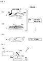
- In this process, however, as shown in conventional steps of FIG. 6, the following steps have been required: resist coating wherein a
resist 2 is coated on a surface of a compound semiconductorsingle crystal 4 on which a silicon oxide film (SiO2) or a silicon nitride film (SiNx) has been deposited, while rotating thesingle crystal 4 at a high speed (STEP1, FIG. 6(A)); then pre-bake wherein solvent and water are got out of the resist film 2 (STEP 2); exposure wherein apattern 6 is printed on theresist film 2 under an ultraviolet light(STEP 3, FIG. 6(B)); development and rinsing wherein thepattern 6 is formed in the resist film 2 (STEP 4, FIG. 6(C)); post-bake wherein a developer and a rinsing liquid is removed from the resist film 2 (STEP 5); and thereafter, etching wherein the oxide film or the nitride film corresponding to theopening pattern 6 is removed by etching (STEP 6). - Thus, since many steps are required for forming a
pattern 6 using the lithographic method in which resist coating and light exposure are repeated and a considerable cost is imposed on each step, there is a limitation on cost down as far as this method is employed. - Further, an influence cannot be neglected on damage of the crystal due to the deposition of the oxide film or the nitride film on the crystal surface and thereby the devices may be affected adversely in terms of their operation. In order to solve a problem of the damage, there has been recently proposed and practiced a method to use as a mask material a natural oxide film on a compound semiconductor readily oxidizable, such as AlGaAs. In this method, however, since such a lithographic method as above described is still adopted, a lot of steps are also required and it is difficult to reduce the number of the steps any more.
- The present invention has been made in view of the above problems, and therefore an object of this invention is to provide a compound semiconductor single crystal and a fabrication process for a compound semiconductor device capable of forming a prescribed pattern without requirement of resist coating.
- In order to solve the above problems, according to the present invention, there is provided a compound semiconductor single crystal, wherein a III-V compound semiconductor single crystal or a II-VI compound semiconductor single crystal includes a region in which a group V element component or a group VI element component is less than a composition ratio expressed by a chemical formula of a corresponding compound semiconductor single crystal.
- Further, a fabrication process for a compound semiconductor device of the present invention comprises: a transmuting step of transmuting part of a surface of a III-V compound semiconductor single crystal or a II-VI compound semiconductor single crystal into a pattern-shaped portion by reducing a group V element component in the III-V compound semiconductor single crystal, or a group VI element component in the II-VI compound semiconductor single crystal less than a composition ratio expressed by a chemical formula of a corresponding compound semiconductor single crystal; and an etching step of effecting selective etching on the corresponding compound semiconductor single crystal.
- The transmuting step is accomplished by imparting energy on the surface of the compound semiconductor single crystal to heat it. Further, the transmuting step may be accomplished by irradiating a laser beam or an electron beam on the surface of the compound semiconductor single crystal. Still further, in the etching step, the surface of the compound semiconductor single crystal transmuted in the transmuting step is preferably used as a protective film.
- Also, a fabrication process for a compound semiconductor device of the present invention comprises: a growth step of forming a III-V compound semiconductor single crystal layer or a II-VI compound semiconductor single crystal layer on a semiconductor single crystal substrate; a transmuting step of irradiating a laser beam on a surface of the compound semiconductor single crystal layer to transmute the surface; and an etching step of effecting selective etching on the compound semiconductor single crystal layer having a region transmuted in the transmuting step to form a protective film.
- The laser beam preferably has energy larger than a bandgap of the compound semiconductor single crystal layer to be irradiated with the laser beam. Further, irradiation power of the laser beam is preferably in the range of from 1 kW/cm2 to 5kW/cm2.
-
- FIG. 1 is a schematic perspective view showing pattern formation steps for a compound semiconductor single crystal of the present invention, wherein (A) and (B) show a laser irradiation step and (C) an etching step;
- FIG. 2 is an explanatory schematic view of a laser beam irradiation apparatus used in Example 1;
- FIG. 3 is a sectional view showing process steps in a pattern formation process in Example 1, wherein (a) shows a compound semiconductor specimen, (b) shows a state of the specimen under irradiation with a laser beam and (c) shows the specimen after etching;
- FIG. 4 is a schematic, partial cross-sectional side view of the laser beam irradiation apparatus used in Example 2;
- FIG. 5 is a sectional view showing steps in a fabrication process for a compound semiconductor light emitting device in Example 2, wherein (a) shows a compound semiconductor single crystal, (b) shows a state of the single crystal under irradiation with a laser beam, (c) shows a state of the single crystal whose GaAs layer has been etched off, (d) shows a state of the single crystal whose AlInP layer has been etched off, (e) shows a state of the single crystal whose GaAs layer has been etched off and (f) shows a state of the single crystal in which a current diffusion layer has been grown.
- FIG. 6 is a schematic perspective view showing pattern formation steps and a flow of typical steps on a compound semiconductor single crystal according to a conventional practice, wherein (A) shows a state of a compound semiconductor single crystal on whose surface a resist is coated, (B) shows an exposure step in which a pattern is defined under ultraviolet irradiation, (C) shows a pattern after developing and rinse and (D) shows a pattern obtained finally.
-
- While description will be given of embodiments of the present invention below, it is needless to say that the descriptions are exemplarily given and should not be construed restrictively.
- As shown in schematic perspective views of processing steps of FIG. 1, a surface 4a of a III-V or II-VI compound semiconductor single crystal 4 (hereinafter may be simply referred to as a single crystal 4) is irradiated, for example, with a laser beam (FIG. 1(A) and FIG.1(B)) and the
single crystal 4 is heated through absorption of the applied laser beam energy. - However, when the laser beam energy is equal to the bandgap of the
single crystal 4 to be irradiated with the laser beam, photoluminescence arises to consume the energy. Further, when the laser beam energy is smaller than the bandgap of thesingle crystal 4, the laser beam is transmitted through thecrystal 4 without absorption. For this reason, the laser beam energy to be applied to thesingle crystal 4 is preferably larger than the bandgap of thesingle crystal 4. - When a III-V or II-VI compound semiconductor
single crystal 4 is irradiated with a laser beam, controlling irradiation power thereof properly, part of a group V element or a group VI element with a high vapor pressure is vaporized as gas from thesingle crystal 4 and therefore in a region irradiated with the laser beam the component of the group V element or the group VI element of thesingle crystal 4 can be lower than the component of the composition ratio expressed by a chemical formula of the compound thereof. - When the III-V compound semiconductor
single crystal 4 is, for example, gallium phosphide, phosphorus with a high vapor pressure is vaporized by applying a laser beam to the gallium phosphide and hence in a region irradiated with the laser beam a composition ratio of phosphorus to gallium becomes lower than 1 : 1 expressed by the chemical formula GaP. - As a result, the surface 4a of the
single crystal 4 is transmuted to a crystal 6a slightly rich in a component of a group III element or a group II element. Since the crystal 6a has a nature akin to group III metals such as Ga, In and Al or group II metals such as Zn and Cd more than thesingle crystal 4, an etching rate is different from that of thesingle crystal 4. Generally, the crystal 6a is more akin to a metal in nature, so its etching rate is smaller than that of thesingle crystal 4. - Then, when the
single crystal 4 is chemically etched using a proper etching liquid, etching does not proceed in a region covered and protected with the transmuted crystal 6a akin to a metal in nature, while etching proceeds selectively in apattern part 6 of the non-transmutedsingle crystal 4, so that it is enable to form a pattern on the single crystal 4 (FIG. 1(C)). - To transmute the crystal 6a to one akin to a metal in nature is achieved by reducing a component of a group V element or a group VI element by about 5 % or more than the composition ration expressed by the chemical formula thereof. The component reduced layer of 0.5 µm or more, preferably 0.1µm or more, can function as a protective film.
- Since the transmuted crystal 6a akin to a metal in nature is hard to be etched, it can function as a protective film in etching of a later step.
- As a laser applicable for transmuting a surface 4a of the
single crystal 4 to the crystal 6a slightly rich in a component of a group III element or a group II element, there may be named a laser capable of vaporizing a group V element or a group VI element, such as an Ar laser, a He-Cd laser and an excimer laser. - A laser actually usable is a laser whose energy is larger than a bandgap of a compound semiconductor single crystal to be irradiated. But He-Cd laser of 325 nm in wavelength is required to be employed for GaN, AlN, AlGaN, InAlN, InGaN and AlGaInN.
- An irradiation power of the above described laser is preferably selected to be in the range of from 1 kW/cm2 to 5 kW/cm2 on a surface of a compound semiconductor single crystal to be irradiated. When the irradiation power is larger than 5 kW/cm2, for example, not only a group V element but also a group III element of the III-V compound semiconductor single crystal are vaporized, so that the single crystal is completely destroyed to form a hole. When the irradiation power is smaller than 1 kW/cm2, vaporization of a group V element or a group VI element is not effected sufficiently and therefore, sufficient transmutation of a compound semiconductor single crystal cannot be achieved. It should be here appreciated that a laser can be employed in the air.
- The following are a list of III-V compound semiconductors transmutable by irradiation with a laser beam. A common feature shared by the III-V compound semiconductors is that arsenic, phosphorus or nitrogen with a high vapor pressure is included as a group V element component.
- GaAs, AlAs, InAs, AlGaAs, AlInAs, InGaAs, GaP, AlP, InP, AlGaP, InGaP, AlInP, AlGaInP, GaAsP, AlAsP, InAsP, AlGaAsP, InGaAsP, AlInAsP, GaN, AlN, InN, AlGaN, AlInN, InGaN, AlGaInN, GaAsN, AlAsN, InAsN, AlGaAsN, InGaAsN and InAlAsN.
- Likewise, there are listed below II-VI compound semiconductors transmutable by irradiation with a laser beam.
- ZnS, ZnSe, ZnTe, CdS, CdSe and CdTe.
- The II-VI compound semiconductors contain sulfur, selenium or tellurium all high in a vapor pressure as a group VI element component and consequently may be transmuted into a crystal slightly rich in a group II element by vaporizing part of a group VI element component with laser beam irradiation.
- While the case of laser beam irradiation has been described in the embodiments of the invention, an electron beam may be also used in a similar way by adjusting an irradiation power thereof.
- A layer whose composition has been transmuted to be akin to a metal in nature may be again applied to an electrically active use as a compound semiconductor layer by heat treating the transmuted layer in an atmosphere for growing the compound semiconductor layer, and with removal of a layer whose composition is transmuted by dry etching or the like, an underlying non-transmuted layer may be also applied to an electrically active use.
- Since a light emitting device in whose current diffusion layer there is formed a current blocking region on whose surface a layer akin to a metal in nature by transmutation of a composition may be fabricated without application of a photolithographic method, the cost thereof is lower. Further, with a laser it is possible to draw a pattern using an inexpensive and simple machine. Further, the present invention may be applied to not only a compound semiconductor layer itself but also an AlGaAs oxide film layer.
- The present invention will be described below in greater detail by way of the following examples. It should be understood that the invention is not limited to the examples and various changes and modification may be made without departing from the technical concept of the invention.
- In practice, a laser
beam irradiation apparatus 12 shown conceptually in FIG. 2 is used. The laserbeam irradiation apparatus 12 includes anAr laser oscillator 14, a reflectingmirror 16, acollective lens 18, and anX-Y stage 19 operable in horizontal directions. - As a
specimen 20, as shown in FIG. 3(a), there is used a compound semiconductor single crystal in which aGaAs buffer layer 24, an AlInP layer 26 (a thickness of about 1.0 µm), and anAlGaAs layer 28 with an Al As mixed crystal ratio of 0.8 (a thickness of about 5.0 µm) are stacked in this order on a GaAssingle crystal substrate 22. An indirect transition bandgap of theAlGaAs layer 28 is about 2.0 eV for an Al As mixed crystal ratio of 0.8. - After the
specimen 20 is placed on theX-Y stage 19, anargon laser beam 14a of energy of 2.4 eV and a wavelength of 514. 5 nm is irradiated for several seconds to each point on a surface of theAlGaAs layer 28, collecting the laser beam by thecollective lens 18 and keeping the irradiation power constant (FIG. 3(b)). - Then in a region irradiated with the laser beam, arsenic included in the
AlGaAs layer 28 is vaporized, and thereby aregion 28a whose As a component is lower than a composition expressed by AlGaAs is formed in theAlGaAs layer 28 of thespecimen 20. - Further, a surface composition of the
AlGaAs layer 28 irradiated with the laser beam is transmuted to the level of a composition of (AlGa)0.525As0.475. Also, for laser irradiation power of 5 kW/cm2, theAlGaAs layer 28 irradiated with the laser beam is presumably transmuted from the surface to a depth of about 3 µm. - Successively, the irradiated
specimen 20 is etched with a mixed etching liquid including sulfuric acid and hydrogen peroxide. Since theAlGaAs layer 28 on the surface of thespecimen 20 is irradiated with thelaser beam 14a to be transmuted to a more metallic state, when etching thespecimen 20 with the mixed etching liquid including sulfuric acid and hydrogen peroxide, while anAlGaAs portion 28a irradiated with the laser beam remains behind, only theAlGaAs portion 28 not irradiated with the laser beam is selectively etched (FIG. 3(c)). - Further, the mixed etching liquid including sulfuric acid and hydrogen peroxide has a higher etching rate to the
AlGaAs layer 28 but a lower etching rate to theAlInP 26 and thus can substantially etch theAlGaAs layer 28 only. Accordingly, if theAlInP layer 26 is provided under theAlGaAs layer 28, the etching can be stopped by theAlInP layer 26. - With the above mentioned procedure, a pattern as shown in FIG. 3(c) can be formed with no resist coating, so that it is possible to fabricate a compound semiconductor device without the need of many steps.
- In this example, a laser
beam irradiation apparatus 30 shown conceptually in FIG. 4 is used. The laserbeam irradiation apparatus 30 includes a finely movableX-Y stage 32, aspecimen fixing holder 34, alaser oscillator 36, acollective lens 38, an X-Ystage control computer 40, a laser spot diametercollective lens 42, avacuum chamber 44, anion pump 46, a turbomolecular pump 48, arotary pump 50, and a reflectingmirror 52. Areference numeral 54 denotes a compound semiconductor material placed on theX-Y stage 32. - The
X-Y stage 32 has a stage which can move stepwise at intervals of 1 µm or less. As a laser beam, there is used an argon laser of energy of 2.4 eV and a wavelength of 514.5 nm. - The
collective lens 38 with magnifying power of 1 to 100 is used. The X-Ystage control computer 40 is capable of programming a drawing pattern. Thecollective lens 42 is capable of collecting light beams into 10 µm to 100 µm in diameter. When thevacuum chamber 44 is provided, a low laser irradiation power can be practically employed. While thevacuum chamber 44 is installed at need, it is possible not to install it. - In FIG. 5, a
compound semiconductor material 54 which is subjected to a series of steps to fabricate a light emitting device is produced as follows. First of all, an n-typeGaAs buffer layer 62 is grown to a thickness of 1 µm on aGaAs substrate 60 with a plane orientation of (001) tilted toward the (111) A plane direction by 5 to 15 degrees. Then, in order to form a double heterostructure layer 63, an n-typeAlInP cladding layer 64 of a thickness of 1 µm, an undoped AlGaInPactive layer 66 of a thickness of 0.6 µm and a p-typeAlInP cladding layer 68 of a thickness of 1 µm are sequentially grown. - Furthermore, in order to form a blocking region 70a, there is grown a
blocking layer 70 including an n-type GaAs layer 72 of a thickness of 0.1 µm, an n-type AlInP layer 74 of a thickness of 1.5 µm and an n-type GaAs layer 76 of a thickness of 0.1 µm. - The blocking region 70a is formed in an n-type and has a opposite conductivity type from a p-type current diffusion layer 78 shown in FIG. 5(f), thus blocking partially a current flowing in the current diffusion layer 78 toward the double heterostructure layer 63 in a light emitting region and concentrating the current within a region other than the blocking region 70a to increase the light emission efficiency. If a cross-sectional area through which a current flows in the current diffusion layer 78 is reduced to, for example, 1/5(one-fifth) by forming the blocking region 70a, a current flowing through a unit cross-sectional area increases five-fold, leading to a five-fold increase in the light emission efficiency.
- A pattern formation on the thus prepared compound semiconductor
single crystal 54 shown in FIG. 5(a) is performed as follows. - First of all, a laser beam of a spot diameter of 10 µm is irradiated in the air over a rectangular area on a surface of the n-type GaAs layer 76 with irradiation power of 5 kW/cm2 on the GaAs layer 76 for an average time of 5 sec. Then part of arsenic with a high vapor pressure is vaporized from the n-type GaAs layer 76 of a thickness of 0.1 µm to form the blocking region 70a transmuted in part of the GaAs layer 76 (FIG. 5(b)).
- Subsequently, a mixed etching liquid composed of 97.2 wt % sulfuric acid : 0.5 wt % hydrogen peroxide : 2.3 wt % pure water is used to selectively etch the GaAs layer 76 at 50°C for 3 minutes and remove the GaAs layer 76 other than the transmuted blocking region 70a (FIG. 5(c)). The blocking region 70a which remained behind after the selective etching functions as a protective film in the following etching steps.
- Next, a mixed etching liquid composed of 30.8 wt % hydrochloric acid : 69.2 wt % pure water is used to etch the
AlInP 74 at 22°C for 1 minute for removing theAlInP layer 74 other than part covered by the blocking region 70a (FIG. 5(d)). - Furthermore, a mixed etching liquid composed of 97.2 wt % sulfuric acid: 0.5 wt % hydrogen peroxide : 2.3 wt % pure water is used to etch the
GaAs layer 72 at 50°C for removing theGaAs layer 72 other than part covered by the blocking region 70a (FIG. 5(e)). - Then, a p-type AlGaAs layer as a current diffusion layer 78 is grown to a thickness of 10 µm on the n-type blocking region 70a (FIG. 5(f)).
- Finally, an n-type electrode is formed on a surface of the
GaAs substrate 60, while a p-type electrode is formed on a surface of the current diffusion layer 78, and as a result a compound semiconductor light emitting device having the blocking region 70a in the current diffusion layer 78 can be fabricated. - As described above, while in the prior art, in order to form a pattern a photolithographic method requiring a lot of steps was indispensably used, according to the present invention, a region is formed in a III-V or II-VI compound semiconductor single crystal to be patterned, in which a group V element component or a group VI element component is less than a composition ratio expressed by a chemical formula of a corresponding compound semiconductor single crystal and therefore, a pattern can be formed without requirement of resist coating, with the result that various devices such as a photodetector, a light emitting device, a high frequency device and a power device, which are fabricated using a compound semiconductor single crystal, can be fabricated with a simple process including the greatly reduced number of steps.
Claims (8)
- A compound semiconductor single crystal, wherein a III-V compound semiconductor single crystal or a II-VI compound semiconductor single crystal includes a region in which a group V element component or a group VI element component is less than a composition ratio expressed by a chemical formula of a corresponding compound semiconductor single crystal.
- A fabrication process for a compound semiconductor device comprising: a transmuting step of transmuting part of a surface of a III-V compound semiconductor single crystal or a II-VI compound semiconductor single crystal into a pattern-shaped portion by reducing a group V element component in the III-V compound semiconductor single crystal, or a group VI element component in the II-VI compound semiconductor single crystal less than a composition ratio expressed by a chemical formula of a corresponding compound semiconductor single crystal; and an etching step of effecting selective etching on the corresponding compound semiconductor single crystal.
- A fabrication process for a compound semiconductor device according to claim 2, wherein the transmuting step is accomplished by imparting energy on the surface of the compound semiconductor single crystal to heat it.
- A fabrication process for a compound semiconductor device according to claim 3, wherein the transmuting step is accomplished by irradiating a laser beam or an electron beam on the surface of the compound semiconductor single crystal.
- A fabrication process for a compound semiconductor device according to any of claims 2 to 4, wherein in the etching step, the surface of the compound semiconductor single crystal transmuted in the transmuting step is used as a protective film.
- A fabrication process for a compound semiconductor device comprising: a growth step of forming a III-V compound semiconductor single crystal layer or a II-VI compound semiconductor single crystal layer on a semiconductor single crystal substrate; a transmuting step of irradiating a laser beam on a surface of the compound semiconductor single crystal layer to transmute the surface; and an etching step of effecting selective etching on the compound semiconductor single crystal layer having a region transmuted in the transmuting step to form a protective film.
- A fabrication process for a compound semiconductor device according to claim 6, wherein the laser beam has energy larger than a bandgap of the compound semiconductor single crystal layer to be irradiated with the laser beam.
- A fabrication process for a compound semiconductor device according to claim 7, wherein irradiation power of the laser beam is in the range of from 1 kW/cm2 to 5kW/cm2.
Applications Claiming Priority (3)
| Application Number | Priority Date | Filing Date | Title |
|---|---|---|---|
| JP11770099 | 1999-04-26 | ||
| JP11770099 | 1999-04-26 | ||
| PCT/JP2000/002683 WO2000065642A1 (en) | 1999-04-26 | 2000-04-25 | Production methods of compound semiconductor single crystal and compound semiconductor element |
Publications (1)
| Publication Number | Publication Date |
|---|---|
| EP1089329A1 true EP1089329A1 (en) | 2001-04-04 |
Family
ID=14718151
Family Applications (1)
| Application Number | Title | Priority Date | Filing Date |
|---|---|---|---|
| EP00917445A Withdrawn EP1089329A1 (en) | 1999-04-26 | 2000-04-25 | Production methods of compound semiconductor single crystal and compound semiconductor element |
Country Status (6)
| Country | Link |
|---|---|
| US (1) | US6589447B1 (en) |
| EP (1) | EP1089329A1 (en) |
| JP (1) | JP3963651B2 (en) |
| KR (1) | KR20010052671A (en) |
| TW (1) | TW463246B (en) |
| WO (1) | WO2000065642A1 (en) |
Cited By (2)
| Publication number | Priority date | Publication date | Assignee | Title |
|---|---|---|---|---|
| WO2020187763A1 (en) * | 2019-03-19 | 2020-09-24 | Osram Opto Semiconductors Gmbh | Method for structuring a semiconductor surface and semiconductor body comprising a semiconductor surface having at least one structure |
| DE102009019281B4 (en) * | 2008-10-14 | 2025-07-24 | Samsung Electronics Co., Ltd. | Surface treatment method for group III nitride semiconductor and method for producing the same |
Families Citing this family (15)
| Publication number | Priority date | Publication date | Assignee | Title |
|---|---|---|---|---|
| JP4329374B2 (en) * | 2002-07-29 | 2009-09-09 | パナソニック電工株式会社 | LIGHT EMITTING ELEMENT AND MANUFACTURING METHOD THEREOF |
| US6932865B2 (en) * | 2003-04-11 | 2005-08-23 | Lockheed Martin Corporation | System and method of making single-crystal structures through free-form fabrication techniques |
| US8562738B2 (en) | 2004-03-11 | 2013-10-22 | Epistar Corporation | Nitride-based light-emitting device |
| US7928424B2 (en) * | 2004-03-11 | 2011-04-19 | Epistar Corporation | Nitride-based light-emitting device |
| US9524869B2 (en) | 2004-03-11 | 2016-12-20 | Epistar Corporation | Nitride-based semiconductor light-emitting device |
| JP2008130818A (en) * | 2006-11-21 | 2008-06-05 | Disco Abrasive Syst Ltd | Laser processing equipment |
| GB2451456B (en) * | 2007-07-31 | 2011-03-02 | Filtronic Compound Semiconductors Ltd | An optical waveguide structure and method of manufacture thereof |
| KR101018179B1 (en) | 2008-10-16 | 2011-02-28 | 삼성엘이디 주식회사 | Pattern formation method of group III nitride semiconductor substrate and manufacturing method of group III nitride semiconductor light emitting device |
| EP2982783A4 (en) | 2013-03-26 | 2017-01-04 | JX Nippon Mining & Metals Corporation | Compound semiconductor wafer, photoelectric conversion element, and method for producing group iii-v compound semiconductor single crystals |
| US11550299B2 (en) | 2020-02-03 | 2023-01-10 | Strong Force TX Portfolio 2018, LLC | Automated robotic process selection and configuration |
| US11669914B2 (en) | 2018-05-06 | 2023-06-06 | Strong Force TX Portfolio 2018, LLC | Adaptive intelligence and shared infrastructure lending transaction enablement platform responsive to crowd sourced information |
| WO2019217323A1 (en) | 2018-05-06 | 2019-11-14 | Strong Force TX Portfolio 2018, LLC | Methods and systems for improving machines and systems that automate execution of distributed ledger and other transactions in spot and forward markets for energy, compute, storage and other resources |
| US11544782B2 (en) | 2018-05-06 | 2023-01-03 | Strong Force TX Portfolio 2018, LLC | System and method of a smart contract and distributed ledger platform with blockchain custody service |
| US12412120B2 (en) | 2018-05-06 | 2025-09-09 | Strong Force TX Portfolio 2018, LLC | Systems and methods for controlling rights related to digital knowledge |
| US11982993B2 (en) | 2020-02-03 | 2024-05-14 | Strong Force TX Portfolio 2018, LLC | AI solution selection for an automated robotic process |
Family Cites Families (7)
| Publication number | Priority date | Publication date | Assignee | Title |
|---|---|---|---|---|
| JPS5534418A (en) * | 1978-09-01 | 1980-03-11 | Ise Electronics Corp | Method of selectively etching semiconductor |
| JPS59177930A (en) * | 1983-03-29 | 1984-10-08 | Oki Electric Ind Co Ltd | Pattern formation of semiconductor device |
| JPS59194439A (en) * | 1983-04-20 | 1984-11-05 | Oki Electric Ind Co Ltd | Method for forming pattern of semiconductor device |
| US4555301A (en) * | 1983-06-20 | 1985-11-26 | At&T Bell Laboratories | Formation of heterostructures by pulsed melting of precursor material |
| US5139606A (en) * | 1989-12-05 | 1992-08-18 | Massachusetts Institute Of Technology | Laser bilayer etching of GaAs surfaces |
| JPH04133327A (en) * | 1990-09-25 | 1992-05-07 | Hikari Keisoku Gijutsu Kaihatsu Kk | Method of finely processing semiconductor |
| US5386798A (en) * | 1993-10-06 | 1995-02-07 | Martin Marietta Energy Systems, Inc. | Method for continuous control of composition and doping of pulsed laser deposited films |
-
2000
- 2000-04-25 US US09/719,545 patent/US6589447B1/en not_active Expired - Fee Related
- 2000-04-25 KR KR1020007013915A patent/KR20010052671A/en not_active Withdrawn
- 2000-04-25 EP EP00917445A patent/EP1089329A1/en not_active Withdrawn
- 2000-04-25 WO PCT/JP2000/002683 patent/WO2000065642A1/en not_active Ceased
- 2000-04-25 JP JP2000614491A patent/JP3963651B2/en not_active Expired - Fee Related
- 2000-04-26 TW TW089107912A patent/TW463246B/en not_active IP Right Cessation
Non-Patent Citations (1)
| Title |
|---|
| See references of WO0065642A1 * |
Cited By (3)
| Publication number | Priority date | Publication date | Assignee | Title |
|---|---|---|---|---|
| DE102009019281B4 (en) * | 2008-10-14 | 2025-07-24 | Samsung Electronics Co., Ltd. | Surface treatment method for group III nitride semiconductor and method for producing the same |
| WO2020187763A1 (en) * | 2019-03-19 | 2020-09-24 | Osram Opto Semiconductors Gmbh | Method for structuring a semiconductor surface and semiconductor body comprising a semiconductor surface having at least one structure |
| US12094928B2 (en) | 2019-03-19 | 2024-09-17 | Osram Opto Semiconductors Gmbh | Method for structuring a semiconductor surface and semiconductor body comprising a semiconductor surface having at least one structure |
Also Published As
| Publication number | Publication date |
|---|---|
| KR20010052671A (en) | 2001-06-25 |
| JP3963651B2 (en) | 2007-08-22 |
| TW463246B (en) | 2001-11-11 |
| WO2000065642A1 (en) | 2000-11-02 |
| US6589447B1 (en) | 2003-07-08 |
Similar Documents
| Publication | Publication Date | Title |
|---|---|---|
| US6589447B1 (en) | Compound semiconductor single crystal and fabrication process for compound semiconductor device | |
| US11942566B2 (en) | Thin-film semiconductor optoelectronic device with textured front and/or back surface prepared from etching | |
| CN100466172C (en) | Method for forming group III nitride semiconductor layer and semiconductor device | |
| US5700703A (en) | Method of fabricating buried control elements in semiconductor devices | |
| US7198970B2 (en) | Technique for perfecting the active regions of wide bandgap semiconductor nitride devices | |
| US5686741A (en) | Compound semiconductor device on silicon substrate and method of manufacturing the same | |
| US8557622B2 (en) | Epitaxial growth of in-plane nanowires and nanowire devices | |
| US6426264B1 (en) | Method of manufacturing a semiconductor laminated substrate, semiconductor crystal substrate and semiconductor device | |
| JPWO2000065642A1 (en) | Compound semiconductor single crystal and method for manufacturing compound semiconductor device | |
| JP2010287805A (en) | Nitride semiconductor device and manufacturing method thereof | |
| US7399684B2 (en) | Defect reduction in semiconductor materials | |
| US8110322B2 (en) | Method of mask forming and method of three-dimensional microfabrication | |
| JP2000150391A (en) | Selective growth method for crystal by focusing ion beam mask work | |
| US5904552A (en) | Method of resistless patterning of a substrate for implantation | |
| Harriott | The technology of finely focused ion beams | |
| KR0185498B1 (en) | Fabrication method of high power quantum thin line array laser diode structure | |
| JP2003332237A (en) | Manufacturing method of semiconductor thin film | |
| US5770475A (en) | Crystal growth method for compound semiconductor | |
| Harriott | In situ processing of semiconductors | |
| JP2711475B2 (en) | Selective epitaxial growth method | |
| Cheng et al. | Aspect ratio trapping heteroepitaxy for integration of germanium and compound semiconductors on silicon | |
| JP2000058454A (en) | Method for forming mask for lateral epitaxial growth and method for lateral epitaxial growth | |
| US5837560A (en) | Method of masking substrates leaving exposed facets | |
| CN118508237A (en) | A method for lateral selective heteroepitaxial high-quality buried quantum well on SOI | |
| JPH06120156A (en) | Method for forming selective epitaxial growth mask |
Legal Events
| Date | Code | Title | Description |
|---|---|---|---|
| PUAI | Public reference made under article 153(3) epc to a published international application that has entered the european phase |
Free format text: ORIGINAL CODE: 0009012 |
|
| 17P | Request for examination filed |
Effective date: 20010123 |
|
| AK | Designated contracting states |
Kind code of ref document: A1 Designated state(s): AT BE CH CY DE DK ES FI FR GB GR IE IT LI LU MC NL PT SE |
|
| RBV | Designated contracting states (corrected) |
Designated state(s): DE FR GB SE |
|
| STAA | Information on the status of an ep patent application or granted ep patent |
Free format text: STATUS: THE APPLICATION IS DEEMED TO BE WITHDRAWN |
|
| 18D | Application deemed to be withdrawn |
Effective date: 20051101 |