EP1089287A1 - Procédé de sélection d'une ligne d'accès à une mémoire, décodeur de ligne d'accès et mémoire l'incorporant. - Google Patents
Procédé de sélection d'une ligne d'accès à une mémoire, décodeur de ligne d'accès et mémoire l'incorporant. Download PDFInfo
- Publication number
- EP1089287A1 EP1089287A1 EP00402335A EP00402335A EP1089287A1 EP 1089287 A1 EP1089287 A1 EP 1089287A1 EP 00402335 A EP00402335 A EP 00402335A EP 00402335 A EP00402335 A EP 00402335A EP 1089287 A1 EP1089287 A1 EP 1089287A1
- Authority
- EP
- European Patent Office
- Prior art keywords
- access
- line
- lines
- access line
- memory
- Prior art date
- Legal status (The legal status is an assumption and is not a legal conclusion. Google has not performed a legal analysis and makes no representation as to the accuracy of the status listed.)
- Withdrawn
Links
- 230000015654 memory Effects 0.000 title claims abstract description 96
- 238000010187 selection method Methods 0.000 title 1
- 238000000034 method Methods 0.000 claims abstract description 21
- 230000004913 activation Effects 0.000 claims abstract description 13
- 230000003247 decreasing effect Effects 0.000 claims abstract 2
- 230000009849 deactivation Effects 0.000 claims description 10
- 230000003213 activating effect Effects 0.000 claims description 6
- 238000013479 data entry Methods 0.000 claims description 6
- 230000009471 action Effects 0.000 claims description 4
- 230000006870 function Effects 0.000 abstract description 10
- 238000010586 diagram Methods 0.000 description 19
- 235000021183 entrée Nutrition 0.000 description 11
- 230000000694 effects Effects 0.000 description 8
- 230000005540 biological transmission Effects 0.000 description 6
- 230000008569 process Effects 0.000 description 5
- XUIMIQQOPSSXEZ-UHFFFAOYSA-N Silicon Chemical compound [Si] XUIMIQQOPSSXEZ-UHFFFAOYSA-N 0.000 description 3
- 239000004020 conductor Substances 0.000 description 3
- 229910052710 silicon Inorganic materials 0.000 description 3
- 239000010703 silicon Substances 0.000 description 3
- 230000006641 stabilisation Effects 0.000 description 3
- 238000011105 stabilization Methods 0.000 description 3
- 239000000758 substrate Substances 0.000 description 3
- 238000006243 chemical reaction Methods 0.000 description 2
- 238000004519 manufacturing process Methods 0.000 description 2
- 238000012163 sequencing technique Methods 0.000 description 2
- 240000008042 Zea mays Species 0.000 description 1
- 230000001174 ascending effect Effects 0.000 description 1
- 230000008859 change Effects 0.000 description 1
- 230000000295 complement effect Effects 0.000 description 1
- 239000011159 matrix material Substances 0.000 description 1
- 230000009467 reduction Effects 0.000 description 1
- 230000033764 rhythmic process Effects 0.000 description 1
- 238000005070 sampling Methods 0.000 description 1
Images


Classifications
-
- G—PHYSICS
- G11—INFORMATION STORAGE
- G11C—STATIC STORES
- G11C5/00—Details of stores covered by group G11C11/00
- G11C5/06—Arrangements for interconnecting storage elements electrically, e.g. by wiring
- G11C5/066—Means for reducing external access-lines for a semiconductor memory clip, e.g. by multiplexing at least address and data signals
-
- G—PHYSICS
- G11—INFORMATION STORAGE
- G11C—STATIC STORES
- G11C8/00—Arrangements for selecting an address in a digital store
- G11C8/10—Decoders
-
- G—PHYSICS
- G11—INFORMATION STORAGE
- G11C—STATIC STORES
- G11C2216/00—Indexing scheme relating to G11C16/00 and subgroups, for features not directly covered by these groups
- G11C2216/12—Reading and writing aspects of erasable programmable read-only memories
- G11C2216/30—Reduction of number of input/output pins by using a serial interface to transmit or receive addresses or data, i.e. serial access memory
Definitions
- the present invention relates to a method of selection of an access line to a circuit memory integrated, of the serial access type, as well as a access line implementing the method and a memory incorporating such a device.
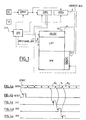
- Memory first includes a memory map MM proper.
- the memory plan consists of a matrix of memory cells produced according to the technology considered.
- a memory cell memorizes the value of a memory bit.
- the cells of the same column are connected to the same connection line, conventionally represented vertically and called bit line.
- cells in the same row are connected to the same connection line, conventionally represented horizontally and called line of words.
- the word lines and the bit lines will also be designated by the expression generic "access line”.
- the memory thus comprises a decoder of ROWDEC word lines and a bit line decoder COLDEC.
- the memory still includes a LAT set of column registers ("Column Register”, in English) cooperating with the bit line decoder for activate bit lines.
- an instruction is received on a serial data input DI of the memory, according to a determined serial transmission protocol (for example the I 2 C protocol, the SPI protocol or the MICROWIRE protocol).
- the binary data of the instruction being transmitted on this input in the form of an electrical signal, they are first of all, in general, reshaped thanks to an input buffer circuit INBUF ("Input Buffer", in English ).
- INBUF input buffer circuit
- such a circuit is not compulsory, and can be omitted in certain applications.
- the following information is contained in the instruction: an operation code (example: write or read), a memory address designating a memory word, and if necessary at least one data word to be written (for a write operation).
- a sequencer SEQ generates control signals adapted to the good management of the memory during the execution of the instruction received.
- the sequencer SEQ receives a clock signal CLK via a clock input CK from the memory.
- the control signals which it generates are schematically represented by arrows in broken lines.
- an address bus ADDRESS_BUS transmits a first part x i of the address of the memory word, called column address, to the bit line decoder COLDEC, and another part y j of the word address memory, called line address, up to the ROWDEC word line decoder.
- the full address of a memory word is coded on eight bits, so that the ADDRESS_BUS bus has eight transmission lines.
- the address is then divided into two parts x i and y j of four bits each, so that the ADDRESS_BUS bus is divided into two parts of four transmission lines each.
- the address register AREG is then an eight-bit register, that is to say that it comprises eight storage flip-flops in series, for the storage respectively of eight address bits received consecutively. It provides a serial / parallel conversion function for the stream of address bits received by the memory via the DI input. Indeed, an output of each of the eight flip-flops of the AREG register is connected respectively to one of the eight transmission lines of the address bus ADDRESS_BUS.
- the instruction data corresponding to the data word to be written are loaded into a shift register DREG input, under the control of the SEQ sequencer.
- the DREG register is an eight-bit register, i.e. that it includes eight storage latches in series, for storing eight bits of data received consecutively.
- the shift register DREG provides a serial / parallel conversion function of the data bit stream received by memory via DI serial data entry. Indeed, an exit from each of the eight flip-flops of the DREG register is linked respectively to one of the eight transmission lines an INPUT_DATA_BUS data input bus.
- the bus INPUT_DATA_BUS is also connected to the LAT assembly column registers to deliver, in the form parallel, eight bits of data. This binary data are loaded into flip-flops for storage and switching of the column register associated with the word memory concerned, under the control of the SEQ sequencer.
- the AREG address register takes up a lot of space on the silicon substrate doped on which memory is performed. This is due to significant number of transistors which compose it. We conceives that this surface occupied by the register at lag is penalizing in terms of cost of manufacturing, especially for low memories capacity (with few bytes stored).
- the invention aims to overcome this drawback of state of the art memories.
- the process according to the invention therefore consists, in a first, to "pre-activate" all lines group access then, in a second time to gradually deactivate the other access lines, according to the bits of the line code of the line to select which are received serially by through the serial data input of the memory, so that, at the end, only the access line to be selected remains activated.
- This method makes unnecessary a shift register such as the register AREG address of Figure 1.
- the invention therefore allows the production of serial access memories occupying less of surface on the doped silicon substrate.
- the invention proposes also such a decoder for the implementation of a process as defined above.
- the invention also provides a memory in integrated circuit, of the serial access type, in particular in EEPROM technology, with data entry series and an actual memory plan which includes memory cells in the form of an array and accessible by a bit line group and a group word lines, characterized in that it comprises a bit line decoder and / or a lines of words of the type mentioned above.
- FIG 2 there is shown the diagram of a flip-flop 10 of an access line decoder according to the invention.
- Such a scale includes means for switching comprising an inverter I1 connected by sound entry to an entry node H and through its exit to a output S of the scale.
- the output S is intended to be connected to a single specific access line of the group of access lines concerned by the decoder.
- the access line In one activated state of the scale, the access line is activated.
- the line access In a disabled state of the scale, the line access is disabled.
- the function of the inverter is to impose said non-zero potential or said potential null on the output S of the rocker when the potential on said input node H of the flip-flop is respectively zero or non-zero.
- the inverter I1 is for example an inverter in CMOS technology, i.e. including a transistor P-type MOS and an N-type MOS transistor, the control grids are common, arranged in series between a non-zero potential V1 and a zero potential constituted by the mass of the integrated circuit. In these conditions, the non-zero potential in question in the paragraph above is said potential V1.
- the memory includes means (not shown) to make the potential V1 equal to one high voltage VPP programming (referenced by relative to the mass), of the order of 18 volts, or to the low supply voltage VCC of the integrated circuit (referenced relative to mass), of the order of 5 volts, or another potential, depending on the operation in progress (reading, programming, or erasure).
- the scale comprises stabilization means, to keep the scale in the deactivated state despite the existence of leakage currents or other phenomena of the same nature.
- These means include a transistor P-type MOS, referenced P2, which is connected by its drain at the input node H, by its source at a potential positive V3, and by its control grid at the output S.
- the transistor P2 ensures a loopback to compensate for possible leakage currents, in order to keep the scale in the deactivated state, therefore that other means do not put it in the state activated.
- these stabilization means only act in the absence of action on the part of others means having them the effect of putting the rocker in the activated state.
- the transistor P2 does not performs its function of keeping the rocker in the deactivated state only in the absence of action by these others means.
- the transistor P2 is very resistive (it has a high resistivity).
- the scale also includes means activation, to put the scale in the state activated, which oppose the stabilization means cited above.
- activation means include a means forming a controlled switch to impose a potential null on the input node H of the rocker.
- This controlled switch is for example a MOS transistor N type referenced N2, connected by its drain to the node input H, by its source to ground, and by its grid command to an input E of the memory.
- this input E can receive a signal RESET initialization active at 1 to force the zero potential on node H.
- Such a transistor has to activate the rocker according to the signal RESET.
- the decoder of access lines has means to put all flip-flops in the activated state preferably simultaneously. These means allow for example apply the aforementioned RESET signal to the inputs E of all the decoder flip-flops, so that all the flip-flops are activated simultaneously.
- the scale also includes means for deactivation, to put the scale in the state disabled.
- deactivation means include decoding means which make it possible to impose a zero potential on the input node H of the flip-flop in function of a line code which is specific to said access line and according to selection signals received by the decoding means, cooperating with additional means to impose a non-zero potential on said input node H of the flip-flop, which act at failure of action of the decoding means. Put another way, the deactivation of the toggle is obtained by the effect of these latter means, unless they are deprived effect by the decoding means.
- the decoding means comprise, in series between the input node H and the ground, p MOS transistors of type N, where p is the number of bits encoding the code of line of an access line.
- p is the number of bits encoding the code of line of an access line.
- these transistors are referenced M0 to M2.
- the control grids of the transistors M0 to M2 are linked to scale selection inputs referenced respectively B0 to B2, to receive each respectively one of three signals of selection Bit0, Bit1, Bit2, or, respectively, Bit0 bar, Bit1 bar, Bit2 bar.
- this is the combination of the signals of selection received on selection inputs B0 to B2 of the toggle which determines the activation conditions of the flip-flop, i.e.
- the means of decoding also include another MOS transistor from type N, referenced N1, whose control grid is connected to the output S of the rocker. The function of this transistor is to make sure that the means of decoding have effect only when the rocker is activated.
- the means to impose a non-zero potential on the rocker input node H include two P-type MOS transistors, referenced P1 and P3, in series between said input node H and a potential positive V2.
- the control gate of transistor P1 is connected to an input G of the scale to receive a DEC signal which by default is 0 so that it conductor the transistor P1.
- the control grid of the transistor P3 is connected to the drain of transistor NI in so that it is at ground zero potential when the toggle is activated, and so that it makes the conductive transistor P3 in this case.
- the potential V2 is for example equal to VCC.
- transistors P1 and P3 are very resistive so that these are then the means of decoding that prevail so that the potential on the input node H is the zero potential of the mass. A weak current flows between VCC and ground in this case. In this way, we can consider that the transistors P1 and P3 do not have the effect of imposing the nonzero potential V2 on the input node H that when the decoding means have no effect, it is to say when one of the transistors M0, M1, M2 or N1 is non-conductive.
- connection connects the input node H to an output F of the rocker on which we will come back to later.
- the potential on the output F is the inverse of the potential on exit S.
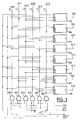
- a decoder of access lines suitable for selection of an access line from a group of eight similar access lines.
- a three-bit line code is associated with each line access (in other words, p is three). It is necessary therefore process three address bits received via the input of memory serial data to select one of access lines. These address bits are nothing else that the line code bits from line to line to select.
- Such a decoder comprises for this purpose eight flip-flops such as the one presented above opposite the Figure 2, which are referenced 100 to 107. These flip-flops are each linked to a group access line of similar access lines. More particularly, the outputs S of these eight rockers are each connected to one of eight access lines, respectively AL0 to AL7. In the case of a decoder bit lines, lines AL0 to AL7 are lines of bits. In the case of a word line decoder, the lines AL0 to AL7 are word lines.
- the decoder also includes means for put all the scales in the activated state. These means preferably include connections for apply the above-mentioned RESET initialization signal to the respective E inputs of all the scales. Of this way, flip-flops 100 to 107 can be activated simultaneously by switching the signal to 1 RESET.
- the decoder also has connections for apply the aforementioned DEC signal to the G inputs respective of all the scales.
- the decoder mainly comprises means for generate the aforementioned selection signals, which are referenced Bit0, Bit1, Bit2, Bit0 bar, Bit1 bar, and Bit2 bar in Figure 3. These means allow generate said selection signals according to access line line code bits to select serial receipts through the serial data input DI from the memory.
- These means include six logic gates of the type NO AND, referenced NE1 to NE6, whose outputs are connected to connection lines respectively L1 to L6, and generate said selection signals Bit0, Bit1, Bit2, Bit0 bar, Bit1 respectively bar, and Bit2 bar.
- synchronization signals CK1 to CK3 are visible on the timing diagrams of figures 4c to 4e respectively. These signals each have a pulse in phase with an address bit respectively 0 to A2 received via the DI serial data input of the memory.
- the DATA bit stream received on this DI input is symbolically represented on the chronogram of the Figure 4a. These are the bits encoding an instruction.
- synchronization signals such as signals CK1 to CK3 already exist in the memories state of the art. They are generated by the SEQ sequencer ( Figure 1) for, specifically, synchronize memory operation, and including, but not limited to, its registry AREG address.
- the invention does not therefore requires no means for the generation of these synchronization signals other than those already present in a memory of known type.
- DATA bit stream received at signal rate CLK clock memory (not shown), say it corresponds to the signal sampling present on the DI serial data input of memory to the rhythm of this signal. It starts with a bit start, referenced START on the timing diagram of the Figure 4a.
- This START bit implies the passage to 1 of the RESET signal visible on the timing diagram of the figure 4b, as shown schematically by an arrow of logical implication.
- the RESET signal stays at most 1 during a signal period clock.
- the three bits of the DATA flow which, in a example, are received between the START bit and the first address bit A0, for example correspond to the code of the operation to be performed in the memory, namely: reading, writing, or whatever.
- bits A0 to A2 are the bits of the access line code at select and are for example included in the address of a memory word from the memory plan to which must relate the operation to be performed.
- the DATA bit stream still has bits coding one or more data to write.
- the DATA bitstream structure depends on the protocol of serial transmission recognized by memory.
- bit A0, then A1 and A2 implies the pulse of the synchronization signal respectively CK1, CK2 and CK3, visible in Figures 4c to 4e respectively. Said pulses correspond to a change to 1 of the synchronization signal concerned for at most one period of the clock signal.
- step a) this step is carried out by changing the RESET signal to 1 as shown on the timing diagram of Figure 4b.
- the transistor N2 of each flip-flop respectively 100 to 107 is returned conductor by this RESET signal so that the node input H of each of the scales is brought to zero potential of the mass.
- the output S of each of the flip-flops is brought to the potential not null V1, i.e. the access line respectively AL0 to AL7 is activated.
- all the lines 100 to 107 are activated simultaneously in step at). This is simpler since a single signal RESET achieves this result.
- step b) the bit Ai of which it is above question is one of the address bits A0 to A2 visible on the timing diagram of Figure 4a. We remember that these are the bits of the line code to select. By convention, we consider that bit A0 is received on the first iteration of step b), the bit A1 on the second iteration, and the bit A2 on the third iteration.
- step c) note that, before reception of the first of bits A0 to A2, every lines L1 to L6 are at 1 since the signals of synchronization CK1, CK2 and CK3 are at 0. So the transistors M0 to M2 of each of the flip-flops respectively 100 to 107 are conductive. However, the transistor N2 of each of the flip-flops respectively 100 to 107 is also conductive since, after step a), all these flip-flops are activated.
- the means for decoding each of the flip-flops respectively 100 to 107 have the effect of imposing the zero potential of the mass on the input node H of each of the scales respectively 100 to 107, the means to impose the nonzero potential V2 on this knots being ineffective due to the strong electrical resistivity of transistors P1 and P3. Said otherwise, the means of decoding each of the scales respectively 100 to 107 take over on the means P1, P3 of each of these flip-flops respectively. Note that the fact that the signal RESET is reset to 0 does not matter.
- j be an index that identifies the j-th iteration of step b) and step c).
- the bit received in series by the memory at this j th iteration of step b) is denoted A j .
- the synchronization signal CK j is in state 1 since it then has a pulse.
- the output of one of the gates NE j or NE j + 3 goes to 0 depending on the value of the bit A j : if A j is 1 then the gate NE j goes to 0; if A j is worth 0 then it is the gate NE j + 3 which passes to 0.
- the line L j or, respectively, the line L j + 3 passes to 0, so that the transistor M j d part of the flip-flops 100 to 107 becomes non-conductive.
- the means of decoding these flip-flops are therefore deprived of effect. Consequently, the means P1, P3 for imposing a non-zero potential on the input node H associated with them act.
- the input node H of these flip-flops is therefore brought to the non-zero potential V2, which amounts to saying that these flip-flops are deactivated.
- the access line (s) which is (are) deactivated in step c) is (are) the access line (s) whose line code has a bit of rank j with a value different from that of bit A j received in the corresponding iteration of step b).
- the bits the code of the access line to be selected received by the memory during successive iterations of step b) are included in the address bits of a memory word memory to be operated on defined by an instruction received according to a protocol determined series.
- memory according to the invention does not include a shift register such as than the AREG register of figure 1, nor of bus address such as the ADDRESS_BUS bus in Figure 1.
- the invention also provides that, the set of access lines being a set ordered, the selection process further comprises a step of activating the access line which, in access line order, follows an access line determined who is selected and then a step of deactivation of said determined access line, in so that’s then said next access line that is selected.
- all of the lines access is ordered in ascending order or descending binary values of line codes which are associated with them respectively.
- An access line decoder conforming to this mode of particular realization, partially represented in the Figure 6, includes means for activating the line which, in the order of the access lines, follows a selected access line that is selected, and means for deactivating said determined access line, so that's the next access line that is selected.
- FIG 6 there is shown in a simplified way three flip - flops 10 i-1 , 10 i and 10 i + 1 respectively coupled to three access lines AL i-1 , AL i and AL i + 1 which follow each other in l 'order of access lines mentioned above.
- ROW i the signal delivered by the output S of the flip-flop 10 i
- SH i the signal delivered by the output F of this flip-flop.
- the signal ROW i is at 1 when the access line AL i is activated and it is at 0 when this access line is deactivated.
- the signal SH i is quite simply the logical inverse of the signal ROW i .
- the aforementioned means of the decoder include, for each flip-flop, on the one hand three MOS transistors of type N referenced respectively NG1, NG2 and NG3, which are connected in series between output F and ground, and on the other hand two N-type MOS transistors referenced respectively ND1 and ND2, which are connected in series between output S and ground.
- the transistor NG1 receives on its control gate the signal ROW i-1
- the transistor NG2 receives on its control gate the signal SH i-2
- the transistor NG3 receives on its control gate a first control signal INCR1
- the transistor ND1 receives on its control gate the signal ROW i + 1
- the transistor ND2 receives on its control gate a second signal INCR2 command.
- the three transistors NG1, NG2 and NG3 carry out the combination of the signals ROW i-1 , SH i-2 , and INCR1 in a logical operation of type ET, to impose the zero potential of the mass on the input node H of the flip-flop, ie to activate the flip-flop, when these three signals are at 1 simultaneously.
- these three transistors are means, controlled by the first control signal INCR1, to activate the access line associated with the flip-flop when the previous access line is activated and the one preceding the latter is not activated.
- the two transistors ND1 and ND2 carry out the logical combination of the signals ROW i + 1 and INCR2 in an AND type operation, to impose the zero potential of the mass on the output S of the flip-flop, it is to say to deactivate the flip-flop, when these two signals are simultaneously at 1.
- these two transistors are means, controlled by the second control signal INCR2, to deactivate an access line associated with the flip-flop when the line d next access is activated.
Landscapes
- Engineering & Computer Science (AREA)
- Microelectronics & Electronic Packaging (AREA)
- Read Only Memory (AREA)
Abstract
Description
- à la figure 1, déjà analysée : le schéma d'une mémoire à accès série selon l'état de la technique ;
- à la figure 2 : le schéma d'une bascule d'un décodeur de ligne d'accès selon l'invention ;
- à la figure 3 : le schéma d'un décodeur de ligne d'accès selon l'invention ;
- aux figures 4a à 4e : des chronogrammes de signaux intervenant dans le fonctionnement du décodeur de la figure 3 ;
- à la figure 5 : le schéma d'une mémoire à accès série selon l'invention;
- à la figure 6 : le schéma de moyens complémentaires du décodeur selon l'invention, permettant la sélection séquentielle des lignes d'accès de la mémoire ;
- aux figures 7a à 7c: des chronogrammes de signaux intervenant dans le fonctionnement des moyens de la figure 6.
- p portes logiques de type NON ET qui, ensemble, reçoivent, sur une première entrée, successivement les p bits du code de ligne reçu, et qui, chacune, reçoivent, sur une seconde entrée, l'un parmi p signaux de synchronisation présentant une impulsion en phase, respectivement, avec le p-ième bit du code de ligne reçu ;
- p autres portes logiques de type NON ET qui, ensemble, reçoivent sur une première entrée, successivement l'inverse logique des p bits du code de ligne reçu, et qui, chacune, reçoivent sur une seconde entrée, l'un parmi p signaux de synchronisation présentant une impulsion en phase, respectivement, avec le p-ième bit du code de ligne reçu.
- l'entrée B0 des bascules 100 à 103 est reliée à la ligne L4 alors que celle des bascules 104 à 107 est reliée à la ligne L1 ;
- l'entrée B1 des bascules 100, 102, 104, 105 est reliée à la ligne L5 alors que celle des bascules 101, 103, 106, et 107 est reliée à la ligne L2 ;
- l'entrée B2 des bascules 100, 101, 104 et 106 est reliée à la ligne L6, alors que celle des bascules 102, 103, 105 et 107 est reliée à la ligne L3.
- dans un premier temps, on génère une impulsion du signal INCR1, par exemple sur une impulsion du signal d'horloge CLK (voir figures 7a et 7b) ; la longueur de cette impulsion est au plus égale à une période du signal d'horloge ; comme les signaux ROWi et SHi-1 sont à 1, la bascule 10i+1 est activée c'est à dire que la ligne d'accès ALi+1 est activée ; on notera que, en plus de la ligne ALi déjà activée, seule cette ligne d'accès ALi+1 est alors activée ; il reste donc à désactiver la ligne ALi pour obtenir le résultat recherché ; c'est ce qu'on fait dans un second temps ;
- en effet, dans un second temps, on génère une impulsion du signal INCR1, par exemple pendant l'impulsion suivante du signal d'horloge CLK (voir figures 7a et 7c) ; la longueur de cette impulsion est au plus égale à une période du signal d'horloge ; comme le signal ROWi+1 est à 1, la bascule 10i est désactivée c'est à dire que la ligne d'accès ALi est désactivée ; on notera que la bascule 10i+1 n'est pas désactivée car le signal ROWi+2 est à 0 ; on notera également que les signaux ROWi et INCR2 étant à 1, ils tendent à désactiver la bascule 10i-1 mais on observe que cela est sans incidence car cette bascule était déjà dans l'état désactivé.
Claims (17)
- Procédé de sélection d'une ligne d'accès déterminée d'une mémoire en circuit intégré à accès série, notamment une mémoire en technologie EEPROM, une ligne d'accès déterminée pouvant être sélectionnée parmi un groupe de lignes d'accès de même nature, par exemple un groupe de lignes de bits ou un groupe de lignes de mots, un code de ligne sur p bits étant respectivement associé à chaque ligne d'accès dudit groupe, caractérisé en ce qu'il comporte les étapes suivantes :les étapes b) et c) étant répétées p fois successivement, respectivement pour chacun des bits du code de ligne reçu par l'intermédiaire de l'entrée de données série (DI) de la mémoire, en sorte qu'à l'issue de ces p itérations des étapes b) et c), seule la ligne d'accès à sélectionner reste activée.a) activation de toutes les lignes d'accès du groupe (AL0-AL7);b) réception, par l'intermédiaire d'une entrée de données série (DI) de la mémoire, d'un bit (Ai) de rang déterminé du code de la ligne d'accès à sélectionner ;c) et, en fonction de la valeur du bit (Ai) reçu à l'étape précédente, désactivation d'une partie des autres lignes d'accès ,
- Procédé selon la revendication 1, caractérisé en ce que, la (ou les) ligne(s) d'accès qui est (sont) désactivée(s) à l'étape c) est (sont) la (les) ligne(s) d'accès dont le code de ligne présente un bit de rang i de valeur différente de celle du bit reçu (Ai) à l'itération correspondante de l'étape b).
- Procédé selon l'une des revendications 1 ou 2, caractérisé en ce que, le groupe de ligne d'accès comprenant 2p lignes d'accès, la moitié des lignes encore activée est désactivée à chaque itération de l'étape c).
- Procédé selon l'une des revendications 1 à 3, caractérisé en ce que, à l'étape a), toutes les lignes d'accès sont activées simultanément.
- Procédé selon l'une des revendications 1 à 4, caractérisé en ce que les bits du code de la ligne d'accès à sélectionner reçus par la mémoire lors des itérations successives de l'étape b) sont compris dans les bits d'adresse d'un mot mémoire de la mémoire sur lequel doit porter une opération définie par une instruction reçue selon un protocole série déterminé.
- Procédé selon l'une des revendications 1 à 5, caractérisé en ce que, l'ensemble des lignes d'accès étant un ensemble ordonné, il comprend de plus une étape d'activation de la ligne d'accès qui, dans l'ordre des lignes d'accès, suit une ligne d'accès déterminée qui est sélectionnée, puis une étape de désactivation de ladite ligne d'accès déterminée, en sorte que c'est alors ladite ligne d'accès suivante qui est sélectionnée.
- Procédé selon la revendication 6, caractérisé en ce que l'ensemble des lignes d'accès est ordonné par l'ordre croissant ou décroissant des valeurs binaires des codes de ligne qui leur sont respectivement associés.
- Décodeur de lignes d'accès pour la mise en oeuvre d'un procédé selon l'une quelconque des revendications 1 à 7, caractérisé en ce qu'il comporte :des bascules, chacune couplée à une ligne d'accès d'un groupe de lignes d'accès de même nature, comprenant chacune des moyens de commutation pour imposer un potentiel non nul sur la ligne d'accès lorsque la bascule est dans un état activé et un potentiel nul lorsqu'elle est dans un état désactivé, des moyens d'activation pour mettre la bascule dans l'état activé, ainsi que des moyens de désactivation pour mettre la bascule dans l'état désactivé en fonction d'un code de ligne qui est propre à ladite ligne d'accès et en fonction de signaux de sélection (Bit0, Bit1, Bit2, Bit0 barre, Bit1 barre, Bit2 barre) reçus par les moyens de désactivation;des moyens pour mettre toutes les bascules dans l'état activé;des moyens pour générer lesdits signaux de sélection (Bit0, Bit1, Bit2, Bit0 barre, Bit1 barre, Bit2 barre) en fonction des bits du code de ligne de la ligne d'accès à sélectionner reçus en série par l'intermédiaire de l'entrée de données série (DI) de la mémoire.
- Décodeur selon la revendication 8, caractérisé en ce que les moyens de commutation d'une bascule comprennent un inverseur dont l'entrée est reliée à un noeud d'entrée (H) de la bascule et dont la sortie est reliée à une sortie (S) de la bascule, pour imposer ledit potentiel non nul ou ledit potentiel nul sur la sortie (S) de la bascule lorsque le potentiel sur ledit noeud d'entrée (H) de la bascule est respectivement nul ou non nul.
- Décodeur selon la revendication 9, caractérisé en ce que les moyens d'activation de la bascule comprennent un moyen formant interrupteur commandé pour imposer un potentiel nul sur ledit noeud d'entrée (H) de la bascule.
- Décodeur selon l'une des revendications 9 ou 10, caractérisé en ce que les moyens de désactivation d'une bascule comprennent des moyens de décodage (M0-M2,N1) qui permettent d'imposer un potentiel nul sur ledit noeud d'entrée (H) de la bascule et des moyens supplétifs pour imposer un potentiel non nul sur ledit noeud d'entrée (H) de la bascule qui agissent à défaut d'action des moyens de décodage.
- Décodeur selon la revendication 11, caractérisé en ce que les moyens de décodage comprennent, en série entre le noeud d'entrée (H) de la bascule et la masse, p transistors MOS de type N (M0-M2) dont les grilles de commande sont reliées à des entrées (B0-B2) de sélection de la bascule pour recevoir au moins certains des signaux de sélection (Bit0, Bit1, Bit2, Bit0 barre, Bit1 barre, Bit2 barre) ainsi qu'un autre transistor MOS de type N (N1) dont la grille de commande est reliée à la sortie (S) de la bascule.
- Décodeur selon l'une quelconque des revendications 8 à 12, caractérisé en ce que les moyens pour générer les signaux de sélection (Bit0, Bit1, Bit2, Bit0 barre, Bit1 barre, Bit2 barre) comprennent :p portes logiques de type NON ET (NEO-NE2) qui, ensemble, reçoivent, sur une première entrée, successivement les p bits du code de ligne reçu, et qui, chacune, reçoivent, sur une seconde entrée, l'un parmi p signaux de synchronisation présentant une impulsion en phase, respectivement, avec le p-ième bit du code de ligne reçu ;p autres portes logiques de type NON ET (NE3-NE5) qui, ensemble, reçoivent sur une première entrée, successivement l'inverse logique des p bits du code de ligne reçu, et qui, chacune, reçoivent sur une seconde entrée, l'un parmi p signaux de synchronisation présentant une impulsion en phase, respectivement, avec le p-ième bit du code de ligne reçu.
- Décodeur selon l'une quelconque des revendications 8 à 13, caractérisé en ce que, l'ensemble des lignes d'accès étant un ensemble ordonné, il comprend des moyens pour activer la ligne d'accès qui, dans l'ordre des lignes d'accès, suit une ligne d'accès déterminée qui est sélectionnée, et des moyens pour désactiver ladite ligne d'accès déterminée, en sorte que c'est alors ladite ligne d'accès suivante qui est sélectionnée.
- Décodeur selon la revendication 14, caractérisé en ce que lesdits moyens pour activer la ligne d'accès qui, dans l'ordre des lignes d'accès, suit une ligne d'accès déterminée qui est sélectionnée, sont des moyens, commandés par un signal de commande (INCR1), pour activer une ligne d'accès lorsque d'une part la ligne d'accès précédente est activée et d'autre part celle qui précède cette dernière n'est pas activée.
- Décodeur selon la revendication 14 ou selon la revendication 15, caractérisé en ce que lesdits moyens pour désactiver ladite ligne d'accès déterminée comprennent des moyens, commandés par un second signal de commande (INCR2), pour désactiver une ligne d'accès lorsque la ligne d'accès suivante est activée.
- Mémoire en circuit intégré, du type à accès série, notamment en technologie EEPROM, comportant une entrée de données série (DI) et un plan mémoire proprement dit (MM) qui comprend des cellules mémoire sous la forme d'une matrice et accessibles par un groupe de ligne de bits et un groupe de lignes de mots, caractérisée en ce qu'elle comprend un décodeur de lignes de bits (COLDEC) et/ou un décodeur de lignes de mots (ROWDEC) selon l'une quelconque des revendications 8 à 16.
Applications Claiming Priority (2)
| Application Number | Priority Date | Filing Date | Title |
|---|---|---|---|
| FR9912148 | 1999-09-29 | ||
| FR9912148A FR2799044B1 (fr) | 1999-09-29 | 1999-09-29 | Procede de selection d'une ligne d'acces a une memoire, decodeur de ligne d'acces et memoire l'incorporant |
Publications (1)
| Publication Number | Publication Date |
|---|---|
| EP1089287A1 true EP1089287A1 (fr) | 2001-04-04 |
Family
ID=9550374
Family Applications (1)
| Application Number | Title | Priority Date | Filing Date |
|---|---|---|---|
| EP00402335A Withdrawn EP1089287A1 (fr) | 1999-09-29 | 2000-08-22 | Procédé de sélection d'une ligne d'accès à une mémoire, décodeur de ligne d'accès et mémoire l'incorporant. |
Country Status (3)
| Country | Link |
|---|---|
| US (1) | US6324117B1 (fr) |
| EP (1) | EP1089287A1 (fr) |
| FR (1) | FR2799044B1 (fr) |
Citations (2)
| Publication number | Priority date | Publication date | Assignee | Title |
|---|---|---|---|---|
| US4680485A (en) * | 1985-06-19 | 1987-07-14 | Gould Inc. | Quad-state control signal input circuit |
| US4972380A (en) * | 1987-06-16 | 1990-11-20 | Mitsubishi Denki Kabushiki Kaisha | Decoding circuit for functional block |
Family Cites Families (2)
| Publication number | Priority date | Publication date | Assignee | Title |
|---|---|---|---|---|
| JPS60142438A (ja) * | 1983-12-28 | 1985-07-27 | Daihatsu Diesel Kk | デ−タログ用外部記憶装置 |
| KR100252056B1 (ko) * | 1997-12-27 | 2000-05-01 | 윤종용 | 반도체 메모리의 어드레스 디코우딩 장치 |
-
1999
- 1999-09-29 FR FR9912148A patent/FR2799044B1/fr not_active Expired - Fee Related
-
2000
- 2000-08-22 EP EP00402335A patent/EP1089287A1/fr not_active Withdrawn
- 2000-09-29 US US09/676,434 patent/US6324117B1/en not_active Expired - Lifetime
Patent Citations (2)
| Publication number | Priority date | Publication date | Assignee | Title |
|---|---|---|---|---|
| US4680485A (en) * | 1985-06-19 | 1987-07-14 | Gould Inc. | Quad-state control signal input circuit |
| US4972380A (en) * | 1987-06-16 | 1990-11-20 | Mitsubishi Denki Kabushiki Kaisha | Decoding circuit for functional block |
Also Published As
| Publication number | Publication date |
|---|---|
| FR2799044A1 (fr) | 2001-03-30 |
| US6324117B1 (en) | 2001-11-27 |
| FR2799044B1 (fr) | 2001-12-14 |
Similar Documents
| Publication | Publication Date | Title |
|---|---|---|
| EP0317014B1 (fr) | Unité de mémoire vive à plusieurs modes de test et ordinateur muni de telles unités | |
| FR2666436A1 (fr) | Memoire a semi-conducteurs a acces rapide. | |
| FR2528613A1 (fr) | Memoire a semi-conducteurs | |
| FR2594275A1 (fr) | Circuit de decalage de niveau pour un convertisseur serie-parallele | |
| FR2619939A1 (fr) | Circuit de detection de transitions d'adresses | |
| FR2707789A1 (fr) | Dispositif de mémoire à semiconducteur pouvant être utilisé comme mémoire tampon de ligne, et procédé de lecture et d'écriture associé. | |
| FR2617621A1 (fr) | Memoire de transposition pour circuit de traitement de donnees | |
| FR2507372A1 (fr) | Dispositif a memoire du type a ecriture-lecture sequentielle et selective a partir d'informations d'adresse | |
| EP0863512B1 (fr) | Mémoire à double accès | |
| FR2504714A1 (fr) | Reseau de memoire a points d'acces multiples | |
| FR2799044A1 (fr) | Procede de selection d'une ligne d'acces a une memoire, decodeur de ligne d'acces et memoire l'incorporant | |
| EP0229433B1 (fr) | Dispositif de test de circuit logique combinatoire | |
| EP0183610A1 (fr) | Mémoire vive et circuit d'interpolation linéaire en comportant application | |
| EP0140413B1 (fr) | Circuit decodeur pour memoire ram statique | |
| FR2623320A1 (fr) | Memoire de type dynamique | |
| EP1089289A1 (fr) | Mémoire en circuit intégré à accès série | |
| EP3018827A1 (fr) | Compteur de gray et convertisseur analogique - numerique utilisant un tel compteur | |
| WO1992015096A1 (fr) | Dispositif d'adressage sequentiel d'une memoire, notamment pour carte a memoire | |
| EP0400734B1 (fr) | Dispositif de retard d'un signal numérique programmable et application à un dispositif de code correcteur d'erreurs | |
| EP0186533B1 (fr) | Elément de mémoire dynamique et son utilisation dans une bascule maître-esclave et dans des circuits séquentiels programmables | |
| FR2986679A1 (fr) | Generateur de nombres aleatoires vrais | |
| EP2777045B1 (fr) | Circuit de polarisation arriere d'inverseurs pour reduction de la consommation d'une mémoire sram | |
| FR2710777A1 (fr) | Dispositif électronique de mémoire à accès séquentiel. | |
| EP1445865A1 (fr) | Diviseur de frequence a structure entonnoir | |
| FR2476893A1 (fr) | Registre a decalage statique i2l |
Legal Events
| Date | Code | Title | Description |
|---|---|---|---|
| PUAI | Public reference made under article 153(3) epc to a published international application that has entered the european phase |
Free format text: ORIGINAL CODE: 0009012 |
|
| AK | Designated contracting states |
Kind code of ref document: A1 Designated state(s): DE FR GB IT |
|
| AX | Request for extension of the european patent |
Free format text: AL;LT;LV;MK;RO;SI |
|
| 17P | Request for examination filed |
Effective date: 20010521 |
|
| RAP1 | Party data changed (applicant data changed or rights of an application transferred) |
Owner name: STMICROELECTRONICS S.A. |
|
| AKX | Designation fees paid |
Free format text: DE FR GB IT |
|
| GRAP | Despatch of communication of intention to grant a patent |
Free format text: ORIGINAL CODE: EPIDOSNIGR1 |
|
| GRAS | Grant fee paid |
Free format text: ORIGINAL CODE: EPIDOSNIGR3 |
|
| STAA | Information on the status of an ep patent application or granted ep patent |
Free format text: STATUS: THE APPLICATION IS DEEMED TO BE WITHDRAWN |
|
| 18D | Application deemed to be withdrawn |
Effective date: 20090303 |