EP1085328A2 - Verfahren zur zeitlichen Markierung von Wellenformen zur Minimalisierung von Digitalisierungsartefakten bei der Messung der Verteilung von Zeitintervallen - Google Patents
Verfahren zur zeitlichen Markierung von Wellenformen zur Minimalisierung von Digitalisierungsartefakten bei der Messung der Verteilung von Zeitintervallen Download PDFInfo
- Publication number
- EP1085328A2 EP1085328A2 EP00307719A EP00307719A EP1085328A2 EP 1085328 A2 EP1085328 A2 EP 1085328A2 EP 00307719 A EP00307719 A EP 00307719A EP 00307719 A EP00307719 A EP 00307719A EP 1085328 A2 EP1085328 A2 EP 1085328A2
- Authority
- EP
- European Patent Office
- Prior art keywords
- time
- time interval
- threshold
- generating
- crossing point
- Prior art date
- Legal status (The legal status is an assumption and is not a legal conclusion. Google has not performed a legal analysis and makes no representation as to the accuracy of the status listed.)
- Granted
Links
- 238000009826 distribution Methods 0.000 title claims abstract description 67
- 238000000034 method Methods 0.000 title claims abstract description 61
- 238000005259 measurement Methods 0.000 title claims description 31
- 230000015654 memory Effects 0.000 description 18
- 238000010586 diagram Methods 0.000 description 5
- 230000000630 rising effect Effects 0.000 description 4
- 230000006870 function Effects 0.000 description 3
- 230000008901 benefit Effects 0.000 description 2
- 238000013139 quantization Methods 0.000 description 2
- 238000005070 sampling Methods 0.000 description 2
- 238000012935 Averaging Methods 0.000 description 1
- 230000007423 decrease Effects 0.000 description 1
- 230000001934 delay Effects 0.000 description 1
- 239000004973 liquid crystal related substance Substances 0.000 description 1
- 230000003287 optical effect Effects 0.000 description 1
- 230000003252 repetitive effect Effects 0.000 description 1
- 230000001629 suppression Effects 0.000 description 1
Images


Classifications
-
- G—PHYSICS
- G01—MEASURING; TESTING
- G01R—MEASURING ELECTRIC VARIABLES; MEASURING MAGNETIC VARIABLES
- G01R13/00—Arrangements for displaying electric variables or waveforms
- G01R13/02—Arrangements for displaying electric variables or waveforms for displaying measured electric variables in digital form
- G01R13/0218—Circuits therefor
- G01R13/0245—Circuits therefor for inserting reference markers
-
- G—PHYSICS
- G01—MEASURING; TESTING
- G01R—MEASURING ELECTRIC VARIABLES; MEASURING MAGNETIC VARIABLES
- G01R13/00—Arrangements for displaying electric variables or waveforms
- G01R13/20—Cathode-ray oscilloscopes
-
- G—PHYSICS
- G01—MEASURING; TESTING
- G01R—MEASURING ELECTRIC VARIABLES; MEASURING MAGNETIC VARIABLES
- G01R13/00—Arrangements for displaying electric variables or waveforms
- G01R13/02—Arrangements for displaying electric variables or waveforms for displaying measured electric variables in digital form
- G01R13/0218—Circuits therefor
- G01R13/0272—Circuits therefor for sampling
-
- G—PHYSICS
- G01—MEASURING; TESTING
- G01R—MEASURING ELECTRIC VARIABLES; MEASURING MAGNETIC VARIABLES
- G01R13/00—Arrangements for displaying electric variables or waveforms
- G01R13/20—Cathode-ray oscilloscopes
- G01R13/22—Circuits therefor
- G01R13/30—Circuits for inserting reference markers, e.g. for timing, for calibrating, for frequency marking
- G01R13/305—Circuits for inserting reference markers, e.g. for timing, for calibrating, for frequency marking for time marking
-
- G—PHYSICS
- G01—MEASURING; TESTING
- G01R—MEASURING ELECTRIC VARIABLES; MEASURING MAGNETIC VARIABLES
- G01R13/00—Arrangements for displaying electric variables or waveforms
- G01R13/20—Cathode-ray oscilloscopes
- G01R13/22—Circuits therefor
- G01R13/34—Circuits for representing a single waveform by sampling, e.g. for very high frequencies
- G01R13/345—Circuits for representing a single waveform by sampling, e.g. for very high frequencies for displaying sampled signals by using digital processors by intermediate A.D. and D.A. convertors (control circuits for CRT indicators)
-
- G—PHYSICS
- G01—MEASURING; TESTING
- G01R—MEASURING ELECTRIC VARIABLES; MEASURING MAGNETIC VARIABLES
- G01R19/00—Arrangements for measuring currents or voltages or for indicating presence or sign thereof
- G01R19/175—Indicating the instants of passage of current or voltage through a given value, e.g. passage through zero
Definitions
- the present invention relates generally to time stamping of threshold crossing points in an acquired waveform input signal where the time stamps are separated by one or more nominal time intervals and more particularly to a method of dithering a threshold level for making time stamp measurements of the crossing points. Such a method is usable in time interval distribution measurements for minimizing digitization artifacts.
- Oscilloscopes are tradition measurement instruments for time interval measurements of an electrical or optical signals, such as pulse width, time period and the like.
- a threshold level is established and the signal crossing points through the threshold are time stamped, such as by placing cursors at the crossing points.
- the time interval between the time stamped locations is calculated and displayed as the time interval measurement.
- Digital oscilloscopes have essentially replaced traditional analog oscilloscopes for measuring electrical signals.
- a digital oscilloscope receives an input analog signal and samples the signal at a defined sample rate established by the instrument setting parameters. The sampled signal is quantized by an analog-to-digital converter to discrete levels and the digitized signal samples are stored in memory.
- a threshold level is established and time marks of the signal crossing points through the threshold are determined by interpolating between signal samples above and below the threshold crossing. The interpolated time marks are used to calculate the time interval between the time marks.
- the computer and telecommunications industry uses digital oscilloscopes to generate statistical time interval distribution measurements for verifying the telecommunications signal meets set standards for jitter.
- a waveform record of the telecommunications signal is acquired and stored.
- a threshold level is set and time stamps are determined for the threshold crossing points using interpolation of data point or points above and below the crossing points.
- Time interval values between time stamps are determined and the statistical time interval distribution measurements are performed.
- a histogram may be made of the time interval values versus the number of occurrences of the each value and displayed as well as a display of the statistical time interval distribution measurements.
- a drawback to using digital oscilloscopes for calculating the time interval of a repetitive electrical signal is artifacts caused by the digitization of the electrical signal. Because quantization levels are fixed, sampled data values above and below the nominal threshold take on a limited set of combinations. This results in time marks that fall at a limited set of interpolated locations between sample points. Time interval measurements made with these time marks will result in a time interval variances. A distribution histogram of the time intervals with digitization artifacts appears as discrete spikes in the plot. This may appear to a user as jitter in the incoming electrical signal where as in fact it is caused by the digitization of the signal.
- One way of reducing the digitization artifact is to add a random amount of noise to the acquired signal samples by dithering the samples.
- a random number generator provides random numbers that are applied to each signal sample. The result of offsetting the signal samples with random numbers is statistically spreading the threshold crossing points of the signal. Even though the time interval distribution is spread out in relation to the digital artifact distribution, the statistical time interval distribution measurements provide a more accurate information on time interval and jitter.
- the above method for reducing digitization artifacts has the drawback of being computationally expensive and/or slow. Random numbers are added to each signal sample. For a digital oscilloscope sampling systems with high sample rates, this add substantial digital processing overhead that is performed by the processor. A separate processor or digital signal processor (DSP) may be used to perform the dithering operation but such an addition adds cost to the oscilloscope.
- DSP digital signal processor
- the time stamping method is usable in generating statistical time interval distribution measurements and histogram displays having reduced the digitization artifacts.
- the present invention is a method for time stamping an input signal having one or more nominal time intervals that is usable for minimizing digitization artifacts in time interval distribution measurements.
- the time stamping method randomly dithers the threshold level to vary the threshold crossing points of the input signal.
- the steps for time stamping includes the steps of establishing a threshold level for measuring a time mark of a threshold crossing point and acquiring digital data samples representative of the input signal prior and subsequent to the threshold crossing.
- the threshold crossing point is determined by interpolating at least a first data sample above and a first data sample below the threshold crossing point.
- the time mark for the interpolated threshold crossing point is stored as the time stamp.
- the threshold level is varied, using threshold offset values, for subsequent threshold crossings of the input signal with digital data samples acquired prior and subsequent to the crossing points interpolated to determine the threshold crossing points.
- the time marks for the crossing points are stored as the time stamps.
- the threshold level establishing includes the further step of generating a distribution threshold values.
- the distribution is a gaussian distribution.
- the interpolating step includes the further step of linearly interpolating between the first data sample above the threshold crossing point and the first data sample below the threshold crossing point.
- a higher order interpolator using multiple data samples above and below the threshold crossing point may be implemented, such as by generating a windowed sin(x)/x function.
- the time stamping method includes the additional steps of generating time interval values defined as the difference between two time stamps and accumulating the number of occurrences of the time interval values in time bins.
- the time interval values may be generated between time stamps in two separate waveforms or between time stamps in a waveform and a set of reference times.
- Further steps include generating and displaying a distribution histogram of the number of occurrences of the time interval values in the accumulated time bins.
- Still further steps include generating and displaying statistical distribution data of the time interval values from the accumulated time bins for mean, standard deviation, and minimum and maximum time intervals.
- the time stamping method is incorporated into a method of minimizing digitization artifacts in time interval distribution measurements on an input signal having one or more nominal time intervals.
- the previously described time stamping method uses a dithered threshold level to generate the time stamps of the input signal threshold crossing points.
- Linear or higher order interpolation such as a windowed sin(x)/x function, are two alternative steps for determining the threshold crossing points.
- the threshold dithering is accomplished by the step of generating a distribution of threshold values. Time interval are generated and the number of occurrences of the time interval values are accumulated in time bins.
- Statistical distribution data is generated from the time bin accumulated time interval values for mean, standard deviation, and minimum and maximum time interval values.
- An additional step includes the display of the statistical distribution data for the time interval values. Further steps include generating and displaying a histogram of the number of occurrences of the time interval values in the time bins.
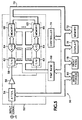
- the functional block diagram includes an analog-to digital (A/D) converter 10 receiving an input signal.
- a threshold time stamp generator 12 receives the digital data samples as well as a initial threshold value from a threshold offset value generator 13.
- the threshold offset value generator 13 has a summing circuit 14 that receives a threshold value and an offset value generated by an offset value generator 15 that produces a distribution of offset values.
- the summing circuit 14 combines the threshold level with the offset values from the offset value generator 15 to produce a dithered threshold value to be described in greater detail below.
- the threshold time stamp generator 12 calculates time stamps for the threshold crossing points of the input signal using the threshold level from the threshold offset value generator.
- a time interval generator 16 receives the calculated time stamps and generates time interval values from the time stamps.
- a time interval accumulator 18 has time bins with selectable bins widths that totals the number of occurrences of the time interval values that fall within each of the bin spans.
- a time interval histogram generator 20 receives the accumulated time interval occurrences from the time bins and generates a graphic representation of the accumulated time interval occurrences versus the time bin values for output to a display.
- a time interval statistical generator 22 also receives the accumulated time interval occurrences from the time bins or the time interval values from the time interval generator via a multiplexer 24. The time interval statistical generator 22 generates statistical data on the time interval values for the mean, standard deviation and minimum and maximum time intervals.
- Figure 1 also shows a dashed line controller 26 and memory 28 connected by a signal and data bus 29 to the A/D converter 10 and functional blocks 12 - 22.
- the digital data samples from the A/D converter 10 are stored in memory 28 and processed by the controller 26, such as microprocessor or the like, under program control that perform the operations of the functional block 12 - 22.
- the dashed elements 26 -29 represent a memory and digital signal processor (DSP) each functional block 12 - 22 for performing the operations of the functional block.
- DSP digital signal processor
- FIG. 2 there is illustrated an acquired input signal waveform 30 having a dithered threshold level used in the method of time stamping an input signal of the present invention.
- Time is in the horizontal direction and magnitude is in the vertical direction.
- the input signal has a first nominal time interval "x" and additional nominal time intervals 2"x" , 3"x", 4"x", ... n”x” that a integer multiples of the first nominal time interval.
- the initial threshold value 32 is shown as a dashed line through the waveform 30.
- Digital data sample points are shown as dots 34 on the waveform 30 with the sample points across the threshold level being shown for each threshold crossing point.
- the sampled data values above and below the nominal threshold value take on a limited set of combinations.
- the resulting time marks fall at a limited set of interpolated locations between the sample points.
- Time interval measurements made with these time marks will show digitization artifacts as graphically shown by the spikes in the time interval histogram of Figure 3.
- the time stamping method of the present invention dithers the threshold level to randomly vary the threshold crossing points of the input signal.
- the resulting time interval distribution of the input signal time intervals statistically spreads out and masks the digitization artifacts. This is graphically shown in the time interval histogram of Figure 4.
- the digital data samples 34 of the input waveform 30 are preferably acquired as a single data record and stored in memory.
- Linear interpolation is performed on at least a first data sample 36 above the threshold crossing point 38 and a first data sample 40 below the threshold crossing point 38 to determine a time mark for the crossing point 38.
- Higher order interpolation may be used for determining the time mark for the crossing point 38, such as a windowed sin(x)/x function using multiple samples above and below the crossing point 38.
- the time mark for the threshold crossing point 38 is stored in memory as the time stamp and the threshold level is randomly dithered for the next threshold crossing point 42.
- the dithering of the threshold level is offset a number of data samples away from the crossing points, as shown at 44.
- the threshold level dithering is preferably accomplished using an offset value generator producing a distribution of random values.
- the offset value generator may be implemented in either hardware or software.
- the offset value generator produces a gaussian distribution of values. Other distributions of the offset values may be used as long as they suppress the digitization artifacts.
- the random values are added to the threshold values to create a new threshold values, such as threshold values 46.
- the digital data samples above and below the new threshold levels are interpolated to produce the time marks for the threshold crossing points and stored as the time stamps of the crossings.
- the dithering of the threshold level and the time stamping of the crossing points are repeated through the waveform record.
- the time stamping of the threshold crossings may occur at less than each crossing point. For example, if one is performing a period time interval measurement, time stamps need only be acquired for every other threshold crossing point.
- the above described time stamping of threshold crossing points using a dithered threshold value substantially decreases the processing time for generating time interval distribution data.
- the frequency of generating a random threshold offset is less than the frequency of generating random data point offsets.
- Dithering a single value, i.e the threshold value is computationally more efficient than dithering all or a portion of the digital data samples.
- the time stamping method the present invention using a dithered threshold level lends itself to real time processing of time interval distribution data.
- FIG. 5 there is shown a representative block diagram of a digital oscilloscope 50 used in implementing the method of time stamping an input signal using a dithered threshold level of the present invention.
- the digital oscilloscope 50 has an acquisition system 52 that may be implemented in a number of ways.
- the input signal is coupled through a variable attenuator 54 and a preamplifier 56.
- each input channel has digitizing pipes, as representatively shown as pipes 58 and 60. Any number of pipes may be included for each oscilloscope input channel.
- Each pipe has a track-and-hold (T/H) circuit 62, an analog-to-digital (A/D) converter 64 and a memory 66.
- a time base 68 provides timing signals to the acquisition system 52 for latching an analog value of the input signal in the T/H circuits 62, clocking the A/D converters 64 to digitize the analog value on the T/H circuit and storing the digitized values in memories 66.
- the pipes 58, 60 have additional circuitry (not shown) that offsets or delays the time base signals for each pipe 58, 60 to produce an acquisition rate "X" times the timing signal rate where "X" is the number of pipes in the acquisition system 52.
- the digital data samples, representative of the input signal are output from the acquisition system 52 via system bus 70.
- Memory 72 is coupled to bus 70 and includes both RAM, ROM and cache memory with the RAM memory storing volatile data, such as the digital data samples of the input signal, calculated time interval values, statistical time interval distribution data, and the like.
- the memory 72 is coupled via the system bus to a controller 74, such as CELERONTM or PENTIUM® microprocessor, manufactured and sold by Intel, Corp., Santa Clara, CA.
- the system bus 70 is also connected to the variable attenuator 54, a display device 76, such a liquid crystal display, cathode ray tube or the like, and a front panel 78 with buttons, rotatable knobs and the like and/or control entry devices, such as a keyboard and/or mouse.
- a mass storage unit or units 80 such as a hard disk drive, CD ROM drive, tape drive, floppy drive or the like that reads from and/or writes to appropriate mass storage media, may also be connected to the system bus 70.
- Program instructions for controlling the digital oscilloscope 50, implementing the time stamping method using a dithered threshold level, and generating time interval distribution histograms and statistical data may be stored and accessed from the ROM memory 72 or from the mass storage media of the mass storage unit 80.
- the digital oscilloscope 50 is a PC based system controlled under WINDOWS® 98 operating system, manufactured and sold by Microsoft, Corp., Redmond, WA.
- the front panel 78 is used to set acquisition and display parameters, such as sample rate, horizontal and vertical scales, and the like, for the digital oscilloscope 50. Additional parameter would include invoking the time interval distribution measurements and setting the bin width for the time interval accumulator and histogram display.
- An input signal such as a 622.8 MHZ or 1.44 MHZ telecommunications signal is coupled to the channel input of the oscilloscope 50.
- the acquisition system 52 is activated to acquire a waveform record of the input signal.
- the digital data samples in the memories 66 of the acquisition system 52 are passed to the system memory 72 via the system bus 70.
- the controller 74 operating under program control from programs stored in memory 72 displays a portion of the stored waveform acquisition.
- a separate display processor may be used to generate displays on display device 76.
- the controller 74 further time stamps the threshold crossing points of the acquired input signal using the dithered threshold levels as previously described. Time interval values are generated using the time stamps and the number of time interval occurrences falling within the respective time bins are accumulated. One or more distribution histograms are generated for the threshold crossing points of the displayed waveform and displayed on display 76 as shown in digital oscilloscope display of Figure 6.
- the controller 74 processes the time interval occurrences in the time bins to generate statistical distribution data on the time intervals including the mean, standard deviation and the minimum and maximum or peak-to-peak time intervals in the distribution data.
- the above described threshold crossing time stamping method and time interval distribution measurements are performed on a input signal that is applied to an input channel of the acquisition system 52 of the digital oscilloscope 50.
- the time stamping method and time interval distribution measurements may also be implemented on multiple waveforms applied to different input channels of the acquisition system 52.
- FIG 7A there is shown a waveform of a clock signal, such as might be generated in a telecommunications system.
- the time stamping method using dithered threshold levels is used to time stamp the threshold crossings of the clock signal.
- Statistical distribution data is generated for the clock signal to establish a mean time interval period "P". Using a fifty percent threshold crossing point as a reference, the threshold crossing times of the clock signal period may be determined.
- Figure 7B shows a data signal that is acquired on a separate input channel of the acquisition system 52.
- the time stamping method using dithered threshold levels is used to time stamp the threshold crossing points of the data signal.
- Statistical distribution data is generated for the data signal to establish a time mean time interval period "P 1 ". Using a fifty percent threshold crossing point as a reference, the threshold crossing times of the data signal period may be determined. The time interval difference between the rising clock edges and the rising data edges can then be determined and stored in time bins for generating a time interval difference distribution histogram.
- Statistical distribution data can also be generated from the time interval difference values.
- Figure 7C shows a reference signal, such as a reference clock signal, for determining time interval differences between the reference clock and a clock signal.
- the reference clock signal may be a set of reference times stored in memory 72 or may be generated from the clock signal of interest.
- the frequency of the clock signal of interest is estimated by averaging a large number of clock periods.
- the estimated clock frequency is used as a reference frequency for the reference signal and the fifty percent crossings are time stamped and stored as reference times.
- the time stamping method using dithered threshold levels is used to time stamp the threshold crossings of the clock signal of interest and statistical distribution data is generated for the clock signal to establish a mean time interval period "P".
- the time interval difference between the rising edges of the clock signal of interest and the reference time of a corresponding rising edge of the reference clock can then be determined and stored in time bins for generating a time interval difference distribution histogram.
- Statistical distribution data can also be generated from the time interval difference values.
- a method has been described for time stamping threshold crossing points of an input signal using a dithered threshold level.
- the threshold level is varied for each threshold crossing of the input signal.
- Digital data samples are acquired for the input signal and time marks are determined for the threshold crossings using interpolation.
- the time marks are stores as the time stamps.
- a threshold offset value generator or the like generates a distribution of offset values for dithering the threshold value.
- the interpolation of the threshold crossing points may be accomplished using linear two point interpolation, multipoint interpolation having more than point above and below the threshold crossing, such as a windowed sin(x)/x interpolation or the like.
- Time interval values are generated from the time stamps.
- the number of occurrences of time interval values are accumulated in time bins and a time interval distribution histogram is generated.
- the accumulated time interval values in the time bins are processed to generate statistical time interval distribution data, such as the mean, standard deviation and minimum and maximum time intervals.
Applications Claiming Priority (2)
| Application Number | Priority Date | Filing Date | Title |
|---|---|---|---|
| US15397899P | 1999-09-14 | 1999-09-14 | |
| US153978P | 1999-09-14 |
Publications (3)
| Publication Number | Publication Date |
|---|---|
| EP1085328A2 true EP1085328A2 (de) | 2001-03-21 |
| EP1085328A3 EP1085328A3 (de) | 2001-08-29 |
| EP1085328B1 EP1085328B1 (de) | 2011-07-06 |
Family
ID=22549516
Family Applications (2)
| Application Number | Title | Priority Date | Filing Date |
|---|---|---|---|
| EP00307719A Expired - Lifetime EP1085328B1 (de) | 1999-09-14 | 2000-09-06 | Verfahren zur zeitlichen Markierung von Wellenformen zur Minimalisierung von Digitalisierungsartefakten bei der Messung der Verteilung von Zeitintervallen |
| EP00307718A Withdrawn EP1085329A3 (de) | 1999-09-14 | 2000-09-06 | Verfahren zur zeitlichen Markierung der Wellenformflanke eines Eingangssignals |
Family Applications After (1)
| Application Number | Title | Priority Date | Filing Date |
|---|---|---|---|
| EP00307718A Withdrawn EP1085329A3 (de) | 1999-09-14 | 2000-09-06 | Verfahren zur zeitlichen Markierung der Wellenformflanke eines Eingangssignals |
Country Status (5)
| Country | Link |
|---|---|
| US (2) | US6571186B1 (de) |
| EP (2) | EP1085328B1 (de) |
| JP (2) | JP3653456B2 (de) |
| KR (2) | KR100681401B1 (de) |
| CN (2) | CN1180265C (de) |
Cited By (5)
| Publication number | Priority date | Publication date | Assignee | Title |
|---|---|---|---|---|
| EP1968832A2 (de) * | 2005-12-22 | 2008-09-17 | Kelsey-Hayes Company | Schattenbereichsfehlererfassung |
| WO2014170172A1 (de) * | 2013-04-15 | 2014-10-23 | Rohde & Schwarz Gmbh & Co. Kg | Messgerät und messverfahren mit mehrfachanzeige |
| DE10223478C5 (de) * | 2001-06-29 | 2018-05-03 | Riegl Laser Measurement Systems Gmbh | Verfahren zur Aufnahme eines Objektraumes |
| EP3508865A1 (de) * | 2018-01-08 | 2019-07-10 | Delta Electronics (Thailand) Public Co., Ltd. | Verfahren zur schätzung einer signaleigenschaft |
| CN114839414A (zh) * | 2022-06-30 | 2022-08-02 | 深圳市鼎阳科技股份有限公司 | 一种用于示波器的采样时间间隔监测装置、方法和示波器 |
Families Citing this family (61)
| Publication number | Priority date | Publication date | Assignee | Title |
|---|---|---|---|---|
| US6621767B1 (en) * | 1999-07-14 | 2003-09-16 | Guide Technology, Inc. | Time interval analyzer having real time counter |
| DE19949647C2 (de) * | 1999-10-14 | 2002-01-31 | Edscha Ag | Türscharnier |
| US20030126258A1 (en) * | 2000-02-22 | 2003-07-03 | Conkright Gary W. | Web based fault detection architecture |
| DE10122905C2 (de) * | 2001-05-11 | 2003-06-05 | Siemens Ag | Verfahren zur prozessgrößenabhängigen Kennsignalausgabe |
| US7268783B2 (en) * | 2001-11-21 | 2007-09-11 | Tektronix, Inc. | Image alias rejection using shaped statistical filtering |
| EP1378854B1 (de) * | 2002-07-01 | 2007-12-26 | Mitsubishi Electric Information Technology Centre Europe B.V. | Bestimmung der statistischen Analyse von Signalen |
| US7437624B2 (en) * | 2002-09-30 | 2008-10-14 | Lecroy Corporation | Method and apparatus for analyzing serial data streams |
| US7519874B2 (en) * | 2002-09-30 | 2009-04-14 | Lecroy Corporation | Method and apparatus for bit error rate analysis |
| US20040123018A1 (en) * | 2002-09-30 | 2004-06-24 | Martin Miller | Method and apparatus for analyzing serial data streams |
| US7236555B2 (en) * | 2004-01-23 | 2007-06-26 | Sunrise Telecom Incorporated | Method and apparatus for measuring jitter |
| US7209864B1 (en) * | 2004-09-09 | 2007-04-24 | Sun Microsystems, Inc. | Method for collecting and reducing performance-related data in constrained environments |
| CA2484951A1 (en) * | 2004-09-27 | 2006-03-27 | Veris Industries, Llc | Method and apparatus for phase determination |
| TWI400460B (zh) * | 2005-11-29 | 2013-07-01 | Tektronix Inc | 傳輸延遲與顫動量測方法 |
| JP4955303B2 (ja) * | 2006-03-23 | 2012-06-20 | テクトロニクス・インコーポレイテッド | デジタル信号分析プログラム及び波形表示装置 |
| DE102006037221B4 (de) * | 2006-08-09 | 2018-07-19 | Rohde & Schwarz Gmbh & Co. Kg | Vorrichtung und Verfahren zur Verarbeitung und Darstellung eines abgetasteten Signals |
| CA2562200A1 (en) * | 2006-09-18 | 2008-03-18 | Abdel-Fattah S. Yousif | Time-to-digital converter |
| US20080222296A1 (en) * | 2007-03-07 | 2008-09-11 | Lisa Ellen Lippincott | Distributed server architecture |
| US8495157B2 (en) * | 2007-03-07 | 2013-07-23 | International Business Machines Corporation | Method and apparatus for distributed policy-based management and computed relevance messaging with remote attributes |
| WO2008109848A2 (en) | 2007-03-07 | 2008-09-12 | Bigfix, Inc. | Pseudo-agent |
| CA2609629A1 (en) * | 2007-09-10 | 2009-03-10 | Veris Industries, Llc | Current switch with automatic calibration |
| CA2609611A1 (en) * | 2007-09-10 | 2009-03-10 | Veris Industries, Llc | Split core status indicator |
| CA2609619A1 (en) | 2007-09-10 | 2009-03-10 | Veris Industries, Llc | Status indicator |
| US7612696B2 (en) * | 2008-03-28 | 2009-11-03 | Motorola, Inc. | Method and system for decimating a pulse width modulated (PWM) signal |
| US8212548B2 (en) | 2008-06-02 | 2012-07-03 | Veris Industries, Llc | Branch meter with configurable sensor strip arrangement |
| US8421443B2 (en) | 2008-11-21 | 2013-04-16 | Veris Industries, Llc | Branch current monitor with calibration |
| US8421639B2 (en) | 2008-11-21 | 2013-04-16 | Veris Industries, Llc | Branch current monitor with an alarm |
| US9335352B2 (en) * | 2009-03-13 | 2016-05-10 | Veris Industries, Llc | Branch circuit monitor power measurement |
| US8966110B2 (en) | 2009-09-14 | 2015-02-24 | International Business Machines Corporation | Dynamic bandwidth throttling |
| WO2011060808A1 (de) * | 2009-11-18 | 2011-05-26 | Siemens Aktiengesellschaft | Anzeigeeinrichtung und verfahren zum anzeigen von messdaten |
| CN102081116B (zh) * | 2009-12-01 | 2013-03-06 | 广芯电子技术(上海)有限公司 | 自适应数字式交流电压过零点检测方法 |
| JP5540959B2 (ja) * | 2010-07-15 | 2014-07-02 | 横河電機株式会社 | 波形測定装置 |
| US10006948B2 (en) | 2011-02-25 | 2018-06-26 | Veris Industries, Llc | Current meter with voltage awareness |
| US9146264B2 (en) | 2011-02-25 | 2015-09-29 | Veris Industries, Llc | Current meter with on board memory |
| US9329996B2 (en) | 2011-04-27 | 2016-05-03 | Veris Industries, Llc | Branch circuit monitor with paging register |
| US9250308B2 (en) | 2011-06-03 | 2016-02-02 | Veris Industries, Llc | Simplified energy meter configuration |
| EP2533423B1 (de) * | 2011-06-06 | 2015-03-04 | Thales Italia S.p.A. | Verfahren zur zeitlich hochgenauen Detektion eines grenzwertüberschreitenden Moments durch ein Signal |
| US8660980B2 (en) | 2011-07-19 | 2014-02-25 | Smartsignal Corporation | Monitoring system using kernel regression modeling with pattern sequences |
| US9250625B2 (en) | 2011-07-19 | 2016-02-02 | Ge Intelligent Platforms, Inc. | System of sequential kernel regression modeling for forecasting and prognostics |
| US9256224B2 (en) | 2011-07-19 | 2016-02-09 | GE Intelligent Platforms, Inc | Method of sequential kernel regression modeling for forecasting and prognostics |
| US8620853B2 (en) | 2011-07-19 | 2013-12-31 | Smartsignal Corporation | Monitoring method using kernel regression modeling with pattern sequences |
| US9410552B2 (en) | 2011-10-05 | 2016-08-09 | Veris Industries, Llc | Current switch with automatic calibration |
| CN102661705B (zh) * | 2012-05-23 | 2014-08-20 | 江西省智成测控技术研究所有限责任公司 | 一种基于异步采样的自适应动态误差补偿方法及补偿装置 |
| CN103869117B (zh) * | 2012-12-13 | 2018-01-16 | 北京普源精电科技有限公司 | 一种波形检测方法及示波器 |
| CN103300846B (zh) * | 2013-05-27 | 2015-03-04 | 北京嘉和美康信息技术有限公司 | 一种波形标记及显示方法、装置 |
| US10408911B2 (en) | 2015-12-28 | 2019-09-10 | Veris Industries, Llc | Network configurable system for a power meter |
| US10371721B2 (en) | 2015-12-28 | 2019-08-06 | Veris Industries, Llc | Configuration system for a power meter |
| US10371730B2 (en) | 2015-12-28 | 2019-08-06 | Veris Industries, Llc | Branch current monitor with client level access |
| US10274572B2 (en) | 2015-12-28 | 2019-04-30 | Veris Industries, Llc | Calibration system for a power meter |
| CN105974171B (zh) * | 2016-04-29 | 2018-09-07 | 深圳市鼎阳科技有限公司 | 一种快速实现线显示的示波器和方法 |
| KR101864837B1 (ko) | 2016-12-14 | 2018-06-12 | 알에프코어 주식회사 | 수신기의 클럭 생성 장치 |
| US11215650B2 (en) | 2017-02-28 | 2022-01-04 | Veris Industries, Llc | Phase aligned branch energy meter |
| US11193958B2 (en) | 2017-03-03 | 2021-12-07 | Veris Industries, Llc | Non-contact voltage sensor |
| US10705126B2 (en) | 2017-05-19 | 2020-07-07 | Veris Industries, Llc | Energy metering with temperature monitoring |
| US20190207830A1 (en) * | 2018-01-02 | 2019-07-04 | Tektronix, Inc. | Network Oscilloscope Using Packet Timestamps |
| EP3564702A1 (de) | 2018-04-30 | 2019-11-06 | Lambda: 4 Entwicklungen GmbH | Verfahren zur verbesserung der laufzeit- und/oder phasenmessung |
| JP7154872B2 (ja) * | 2018-08-10 | 2022-10-18 | 横河電機株式会社 | デジタルオシロスコープ及びその制御方法 |
| CN109633236B (zh) * | 2018-12-13 | 2021-06-22 | 成都精位科技有限公司 | 无线电信号识别方法及装置 |
| CN111122951B (zh) * | 2019-12-16 | 2021-12-28 | 上海卫星工程研究所 | 一种火工品点火电流检测方法 |
| CN114371642A (zh) * | 2019-12-24 | 2022-04-19 | 追觅科技(上海)有限公司 | 设备控制方法、装置及存储介质 |
| CN113449264B (zh) * | 2020-03-27 | 2023-08-15 | 中国移动通信集团设计院有限公司 | 波形边缘的监测方法及装置 |
| US20220043031A1 (en) * | 2020-08-06 | 2022-02-10 | Rohde & Schwarz Gmbh & Co. Kg | Method of analyzing a signal and signal analysis device |
Citations (6)
| Publication number | Priority date | Publication date | Assignee | Title |
|---|---|---|---|---|
| US4584690A (en) * | 1984-05-07 | 1986-04-22 | D.A.V.I.D. Systems, Inc. | Alternate Mark Invert (AMI) transceiver with switchable detection and digital precompensation |
| US4647968A (en) * | 1984-12-03 | 1987-03-03 | Rca Corporation | Analog-to-digital conversion system as for a narrow bandwidth signal processor |
| FR2610413A1 (fr) * | 1987-01-29 | 1988-08-05 | Bosch Gmbh Robert | Dispositif pour la determination de points precis de declenchement d'un signal d'emission electrique repetitif indicateur d'incident |
| US5446650A (en) * | 1993-10-12 | 1995-08-29 | Tektronix, Inc. | Logic signal extraction |
| US5578928A (en) * | 1995-01-23 | 1996-11-26 | General Electric Company | Method for detecting zero crossings in a rectified power signal |
| US5862185A (en) * | 1994-07-21 | 1999-01-19 | Tektronix, Inc. | Data signal zero crossing detection process |
Family Cites Families (27)
| Publication number | Priority date | Publication date | Assignee | Title |
|---|---|---|---|---|
| US4364080A (en) * | 1981-04-13 | 1982-12-14 | Jovan Vidovic | Digital video analyzer |
| US4553091A (en) * | 1983-02-07 | 1985-11-12 | Tektronix, Inc. | Automatic vertical calibration method and system for an oscilloscope |
| US4710747A (en) * | 1984-03-09 | 1987-12-01 | Fairchild Semiconductor Corporation | Method and apparatus for improving the accuracy and resolution of an analog-to-digital converter (ADC) |
| US4704558A (en) * | 1985-12-02 | 1987-11-03 | Tektronix, Inc. | Method and apparatus for automatic oscilloscope calibration |
| US4743844A (en) * | 1986-12-19 | 1988-05-10 | Tektronix, Inc. | Self-adjusting oscilloscope |
| US5233545A (en) * | 1989-09-19 | 1993-08-03 | Hewlett-Packard Company | Time interval triggering and hardware histogram generation |
| US5212485A (en) * | 1990-09-27 | 1993-05-18 | Tektronix, Inc. | Analog oscilloscope digitizer |
| US5115189A (en) * | 1991-02-06 | 1992-05-19 | Hewlett-Packard Company | Anti-aliasing dithering method and apparatus for low frequency signal sampling |
| JP3144563B2 (ja) * | 1991-02-18 | 2001-03-12 | 横河電機株式会社 | 波形測定装置 |
| US5392037A (en) * | 1991-05-21 | 1995-02-21 | Matsushita Electric Industrial Co., Ltd. | Method and apparatus for encoding and decoding |
| JPH05119070A (ja) * | 1991-09-30 | 1993-05-14 | Yokogawa Electric Corp | デイジタルオシロスコープ |
| US5519625A (en) * | 1994-02-16 | 1996-05-21 | Hewlett-Packard Company | System for characterizing phase-modulated signals using a time interval analyzer |
| US5508605A (en) * | 1994-05-24 | 1996-04-16 | Alliedsignal Inc. | Method for measuring RF pulse frequency |
| US5514865A (en) * | 1994-06-10 | 1996-05-07 | Westinghouse Electric Corp. | Dither image scanner with compensation for individual detector response and gain correction |
| US5495168A (en) * | 1994-09-12 | 1996-02-27 | Fluke Corporation | Method of signal analysis employing histograms to establish stable, scaled displays in oscilloscopes |
| US5805460A (en) * | 1994-10-21 | 1998-09-08 | Alliedsignal Inc. | Method for measuring RF pulse rise time, fall time and pulse width |
| US5680870A (en) * | 1995-01-04 | 1997-10-28 | Johnson & Johnson Medical, Inc. | Oscillometric blood pressure monitor which acquires blood pressure signals from composite arterial pulse signal |
| US6263290B1 (en) * | 1995-02-22 | 2001-07-17 | Michael K. Williams | Process and machine for signal waveform analysis |
| GB9505540D0 (en) * | 1995-03-18 | 1995-05-03 | Sun Electric Uk Ltd | Method and apparatus for engine analysis |
| US5764524A (en) * | 1996-02-12 | 1998-06-09 | Snap-On Technologies, Inc. | Method and apparatus for detection of missing pulses from a repetitive pulse train |
| US5877621A (en) * | 1996-04-30 | 1999-03-02 | Hewlett-Packard Company | Digital oscilloscope with pan and zoom produced from time stamped data records indexed by trigger offset |
| US5809177A (en) * | 1996-06-06 | 1998-09-15 | Xerox Corporation | Hybrid error diffusion pattern shifting reduction using programmable threshold perturbation |
| JPH1038927A (ja) * | 1996-07-23 | 1998-02-13 | Advantest Corp | 波形解析装置 |
| US5978742A (en) * | 1997-04-04 | 1999-11-02 | Tektronix, Inc. | Method and apparatus for digital sampling of electrical waveforms |
| US6269317B1 (en) * | 1997-04-30 | 2001-07-31 | Lecroy Corporation | Self-calibration of an oscilloscope using a square-wave test signal |
| CA2242622A1 (en) * | 1997-07-10 | 1999-01-10 | Universite Laval | Integrated motion vision sensor |
| US6208871B1 (en) * | 1998-02-27 | 2001-03-27 | Motorola, Inc. | Method and apparatus for providing a time adjustment to a wireless communication system |
-
2000
- 2000-08-31 US US09/652,939 patent/US6571186B1/en not_active Expired - Fee Related
- 2000-09-05 US US09/654,665 patent/US6549859B1/en not_active Expired - Fee Related
- 2000-09-06 EP EP00307719A patent/EP1085328B1/de not_active Expired - Lifetime
- 2000-09-06 EP EP00307718A patent/EP1085329A3/de not_active Withdrawn
- 2000-09-14 CN CNB001313967A patent/CN1180265C/zh not_active Expired - Fee Related
- 2000-09-14 JP JP2000280532A patent/JP3653456B2/ja not_active Expired - Lifetime
- 2000-09-14 JP JP2000280533A patent/JP3805181B2/ja not_active Expired - Fee Related
- 2000-09-14 KR KR1020000054013A patent/KR100681401B1/ko not_active IP Right Cessation
- 2000-09-14 CN CNB001313819A patent/CN1187620C/zh not_active Expired - Fee Related
- 2000-09-14 KR KR1020000054078A patent/KR100694010B1/ko not_active IP Right Cessation
Patent Citations (6)
| Publication number | Priority date | Publication date | Assignee | Title |
|---|---|---|---|---|
| US4584690A (en) * | 1984-05-07 | 1986-04-22 | D.A.V.I.D. Systems, Inc. | Alternate Mark Invert (AMI) transceiver with switchable detection and digital precompensation |
| US4647968A (en) * | 1984-12-03 | 1987-03-03 | Rca Corporation | Analog-to-digital conversion system as for a narrow bandwidth signal processor |
| FR2610413A1 (fr) * | 1987-01-29 | 1988-08-05 | Bosch Gmbh Robert | Dispositif pour la determination de points precis de declenchement d'un signal d'emission electrique repetitif indicateur d'incident |
| US5446650A (en) * | 1993-10-12 | 1995-08-29 | Tektronix, Inc. | Logic signal extraction |
| US5862185A (en) * | 1994-07-21 | 1999-01-19 | Tektronix, Inc. | Data signal zero crossing detection process |
| US5578928A (en) * | 1995-01-23 | 1996-11-26 | General Electric Company | Method for detecting zero crossings in a rectified power signal |
Cited By (9)
| Publication number | Priority date | Publication date | Assignee | Title |
|---|---|---|---|---|
| DE10223478C5 (de) * | 2001-06-29 | 2018-05-03 | Riegl Laser Measurement Systems Gmbh | Verfahren zur Aufnahme eines Objektraumes |
| EP1968832A2 (de) * | 2005-12-22 | 2008-09-17 | Kelsey-Hayes Company | Schattenbereichsfehlererfassung |
| EP1968832A4 (de) * | 2005-12-22 | 2013-03-13 | Kelsey Hayes Co | Schattenbereichsfehlererfassung |
| WO2014170172A1 (de) * | 2013-04-15 | 2014-10-23 | Rohde & Schwarz Gmbh & Co. Kg | Messgerät und messverfahren mit mehrfachanzeige |
| US11054445B2 (en) | 2013-04-15 | 2021-07-06 | Rohde & Schwarz Gmbh & Co. Kg | Measuring device and measuring method with multiple display |
| EP3508865A1 (de) * | 2018-01-08 | 2019-07-10 | Delta Electronics (Thailand) Public Co., Ltd. | Verfahren zur schätzung einer signaleigenschaft |
| US11131696B2 (en) | 2018-01-08 | 2021-09-28 | Delta Electronics (Thailand) Public Co., Ltd. | Method for estimating a signal property |
| CN114839414A (zh) * | 2022-06-30 | 2022-08-02 | 深圳市鼎阳科技股份有限公司 | 一种用于示波器的采样时间间隔监测装置、方法和示波器 |
| CN114839414B (zh) * | 2022-06-30 | 2022-09-06 | 深圳市鼎阳科技股份有限公司 | 一种用于示波器的采样时间间隔监测装置、方法和示波器 |
Also Published As
| Publication number | Publication date |
|---|---|
| EP1085329A3 (de) | 2001-08-29 |
| KR20010050448A (ko) | 2001-06-15 |
| JP3805181B2 (ja) | 2006-08-02 |
| US6571186B1 (en) | 2003-05-27 |
| KR100694010B1 (ko) | 2007-03-12 |
| KR20010050459A (ko) | 2001-06-15 |
| KR100681401B1 (ko) | 2007-02-09 |
| JP2001147242A (ja) | 2001-05-29 |
| JP3653456B2 (ja) | 2005-05-25 |
| CN1290860A (zh) | 2001-04-11 |
| CN1187620C (zh) | 2005-02-02 |
| JP2001141752A (ja) | 2001-05-25 |
| EP1085329A2 (de) | 2001-03-21 |
| EP1085328A3 (de) | 2001-08-29 |
| EP1085328B1 (de) | 2011-07-06 |
| CN1289047A (zh) | 2001-03-28 |
| CN1180265C (zh) | 2004-12-15 |
| US6549859B1 (en) | 2003-04-15 |
Similar Documents
| Publication | Publication Date | Title |
|---|---|---|
| US6571186B1 (en) | Method of waveform time stamping for minimizing digitization artifacts in time interval distribution measurements | |
| EP0701138B1 (de) | Signalanalyseverfahren mit Hilfe von Histogrammen | |
| JP2733746B2 (ja) | ロジック信号表示方法 | |
| US4495586A (en) | Waveform acquisition apparatus and method | |
| US6263290B1 (en) | Process and machine for signal waveform analysis | |
| US6681191B1 (en) | Frequency domain analysis system for a time domain measurement instrument | |
| US8332172B2 (en) | System for independently modifying jitter and noise components in a signal digitizing instrument | |
| US8155165B2 (en) | Method of characterizing parameters and removing spectral components of a spread spectrum clock in a communications signal | |
| JPH0219653B2 (de) | ||
| EP1118866A1 (de) | Verfahren zur Schätzung der Störphasen eines Leistungsspektrums und Jitter eines periodischen Signals | |
| US6121799A (en) | Interleaved digital peak detector | |
| JPH0635996B2 (ja) | デ−タ分布測定装置 | |
| JP2591965B2 (ja) | オシロスコープの掃引方法 | |
| US5352976A (en) | Multi-channel trigger dejitter | |
| EP1111396A2 (de) | Frequenzbereich-Analysesystem für ein Zeitbereich-Messinstrument | |
| US6998834B2 (en) | Real-time time drift adjustment for a TDR step stimulus | |
| EP0225704A2 (de) | Methode und Einrichtung zur Analyse der Wellenform | |
| Haney | Maximizing the measurement accuracy of digitized signals |
Legal Events
| Date | Code | Title | Description |
|---|---|---|---|
| PUAI | Public reference made under article 153(3) epc to a published international application that has entered the european phase |
Free format text: ORIGINAL CODE: 0009012 |
|
| AK | Designated contracting states |
Kind code of ref document: A2 Designated state(s): AT BE CH CY DE DK ES FI FR GB GR IE IT LI LU MC NL PT SE |
|
| AX | Request for extension of the european patent |
Free format text: AL;LT;LV;MK;RO;SI |
|
| PUAL | Search report despatched |
Free format text: ORIGINAL CODE: 0009013 |
|
| AK | Designated contracting states |
Kind code of ref document: A3 Designated state(s): AT BE CH CY DE DK ES FI FR GB GR IE IT LI LU MC NL PT SE |
|
| AX | Request for extension of the european patent |
Free format text: AL;LT;LV;MK;RO;SI |
|
| 17P | Request for examination filed |
Effective date: 20020226 |
|
| AKX | Designation fees paid |
Free format text: DE FR GB IT |
|
| 17Q | First examination report despatched |
Effective date: 20061204 |
|
| GRAP | Despatch of communication of intention to grant a patent |
Free format text: ORIGINAL CODE: EPIDOSNIGR1 |
|
| GRAS | Grant fee paid |
Free format text: ORIGINAL CODE: EPIDOSNIGR3 |
|
| GRAA | (expected) grant |
Free format text: ORIGINAL CODE: 0009210 |
|
| AK | Designated contracting states |
Kind code of ref document: B1 Designated state(s): DE FR GB IT |
|
| REG | Reference to a national code |
Ref country code: GB Ref legal event code: FG4D |
|
| REG | Reference to a national code |
Ref country code: DE Ref legal event code: R096 Ref document number: 60046169 Country of ref document: DE Effective date: 20110825 |
|
| PLBE | No opposition filed within time limit |
Free format text: ORIGINAL CODE: 0009261 |
|
| STAA | Information on the status of an ep patent application or granted ep patent |
Free format text: STATUS: NO OPPOSITION FILED WITHIN TIME LIMIT |
|
| 26N | No opposition filed |
Effective date: 20120411 |
|
| REG | Reference to a national code |
Ref country code: DE Ref legal event code: R097 Ref document number: 60046169 Country of ref document: DE Effective date: 20120411 |
|
| PGFP | Annual fee paid to national office [announced via postgrant information from national office to epo] |
Ref country code: GB Payment date: 20120920 Year of fee payment: 13 |
|
| PGFP | Annual fee paid to national office [announced via postgrant information from national office to epo] |
Ref country code: DE Payment date: 20120921 Year of fee payment: 13 |
|
| PGFP | Annual fee paid to national office [announced via postgrant information from national office to epo] |
Ref country code: FR Payment date: 20121010 Year of fee payment: 13 |
|
| PGFP | Annual fee paid to national office [announced via postgrant information from national office to epo] |
Ref country code: IT Payment date: 20120927 Year of fee payment: 13 |
|
| GBPC | Gb: european patent ceased through non-payment of renewal fee |
Effective date: 20130906 |
|
| REG | Reference to a national code |
Ref country code: FR Ref legal event code: ST Effective date: 20140530 |
|
| REG | Reference to a national code |
Ref country code: DE Ref legal event code: R119 Ref document number: 60046169 Country of ref document: DE Effective date: 20140401 |
|
| PG25 | Lapsed in a contracting state [announced via postgrant information from national office to epo] |
Ref country code: GB Free format text: LAPSE BECAUSE OF NON-PAYMENT OF DUE FEES Effective date: 20130906 |
|
| PG25 | Lapsed in a contracting state [announced via postgrant information from national office to epo] |
Ref country code: FR Free format text: LAPSE BECAUSE OF NON-PAYMENT OF DUE FEES Effective date: 20130930 Ref country code: DE Free format text: LAPSE BECAUSE OF NON-PAYMENT OF DUE FEES Effective date: 20140401 Ref country code: IT Free format text: LAPSE BECAUSE OF NON-PAYMENT OF DUE FEES Effective date: 20130906 |