EP1083672B1 - High-frequency switch module - Google Patents
High-frequency switch module Download PDFInfo
- Publication number
- EP1083672B1 EP1083672B1 EP00909731A EP00909731A EP1083672B1 EP 1083672 B1 EP1083672 B1 EP 1083672B1 EP 00909731 A EP00909731 A EP 00909731A EP 00909731 A EP00909731 A EP 00909731A EP 1083672 B1 EP1083672 B1 EP 1083672B1
- Authority
- EP
- European Patent Office
- Prior art keywords
- circuit
- distributed constant
- diode
- filter
- constant line
- Prior art date
- Legal status (The legal status is an assumption and is not a legal conclusion. Google has not performed a legal analysis and makes no representation as to the accuracy of the status listed.)
- Expired - Lifetime
Links
Images


Classifications
-
- H—ELECTRICITY
- H01—ELECTRIC ELEMENTS
- H01P—WAVEGUIDES; RESONATORS, LINES, OR OTHER DEVICES OF THE WAVEGUIDE TYPE
- H01P1/00—Auxiliary devices
- H01P1/20—Frequency-selective devices, e.g. filters
- H01P1/213—Frequency-selective devices, e.g. filters combining or separating two or more different frequencies
- H01P1/2135—Frequency-selective devices, e.g. filters combining or separating two or more different frequencies using strip line filters
-
- H—ELECTRICITY
- H01—ELECTRIC ELEMENTS
- H01P—WAVEGUIDES; RESONATORS, LINES, OR OTHER DEVICES OF THE WAVEGUIDE TYPE
- H01P1/00—Auxiliary devices
- H01P1/10—Auxiliary devices for switching or interrupting
- H01P1/15—Auxiliary devices for switching or interrupting by semiconductor devices
-
- H—ELECTRICITY
- H04—ELECTRIC COMMUNICATION TECHNIQUE
- H04B—TRANSMISSION
- H04B1/00—Details of transmission systems, not covered by a single one of groups H04B3/00 - H04B13/00; Details of transmission systems not characterised by the medium used for transmission
- H04B1/005—Details of transmission systems, not covered by a single one of groups H04B3/00 - H04B13/00; Details of transmission systems not characterised by the medium used for transmission adapting radio receivers, transmitters andtransceivers for operation on two or more bands, i.e. frequency ranges
- H04B1/0053—Details of transmission systems, not covered by a single one of groups H04B3/00 - H04B13/00; Details of transmission systems not characterised by the medium used for transmission adapting radio receivers, transmitters andtransceivers for operation on two or more bands, i.e. frequency ranges with common antenna for more than one band
- H04B1/0057—Details of transmission systems, not covered by a single one of groups H04B3/00 - H04B13/00; Details of transmission systems not characterised by the medium used for transmission adapting radio receivers, transmitters andtransceivers for operation on two or more bands, i.e. frequency ranges with common antenna for more than one band using diplexing or multiplexing filters for selecting the desired band
-
- H—ELECTRICITY
- H04—ELECTRIC COMMUNICATION TECHNIQUE
- H04B—TRANSMISSION
- H04B1/00—Details of transmission systems, not covered by a single one of groups H04B3/00 - H04B13/00; Details of transmission systems not characterised by the medium used for transmission
- H04B1/38—Transceivers, i.e. devices in which transmitter and receiver form a structural unit and in which at least one part is used for functions of transmitting and receiving
- H04B1/40—Circuits
- H04B1/44—Transmit/receive switching
- H04B1/48—Transmit/receive switching in circuits for connecting transmitter and receiver to a common transmission path, e.g. by energy of transmitter
-
- H—ELECTRICITY
- H04—ELECTRIC COMMUNICATION TECHNIQUE
- H04B—TRANSMISSION
- H04B1/00—Details of transmission systems, not covered by a single one of groups H04B3/00 - H04B13/00; Details of transmission systems not characterised by the medium used for transmission
- H04B1/38—Transceivers, i.e. devices in which transmitter and receiver form a structural unit and in which at least one part is used for functions of transmitting and receiving
- H04B1/40—Circuits
- H04B1/44—Transmit/receive switching
Definitions
- the present invention relates to a high-frequency switch module for wireless communications equipment adapted for three different communication modes.
- GSM Global System for Mobile Communications
- DCS1800 Digital Cellular System 1800
- PCS Personal Communications Services
- PDC Personal Digital Cellular
- High-frequency circuit parts are needed for each system, for instance, a filter for passing a transmission signal of a desired transmission frequency, a high-frequency switch for switching a transmission circuit and a reception circuit and an antenna for emitting a transmission signal and receiving a reception signal in a transmission system; and a filter for passing a signal of a desired frequency among reception signals passing through the high-frequency switch in a reception system.
- an object of the present invention is to provide a miniaturized, high-performance, high-frequency switch module capable of switching transmission circuits and reception circuits of a plurality of systems (particularly three systems) with high-frequency switches, as a high-frequency circuit part used in a portable communications equipment, which permits a single portable communications equipment to be compatible with a plurality of systems.
- EP-A-0 820 155 discloses a duplexer including a high frequency switch, an LC filter serving as a low-pass filter, and an SAW filter serving as a band-pass filter.
- the device of this document does not include a second switch circuit connected between the second filter and a transmission circuit.
- EP-A-1 003 291 and EP-A-1 014 592 disclose further relevant HF switch circuits. These two documents have been published after the filing date of the present invention, and belong to the state of the art under Article 54(3) EPC.
- the high-frequency switch module for switching a transmission circuit and a reception circuit in each of a plurality of different transmitting and receiving systems according to the present invention is defined in appended claim 1.
- the subclaims relate to preferred embodiments.
- the first and second filter circuits function as branching filter circuits for dividing a reception signal for the first transmitting and receiving system and a reception signal for the second and third transmitting and receiving systems.
- the first distributed constant line preferably has a line length in which a resonance frequency thereof is within a range between the maximum frequency and the minimum frequency in a frequency band of the transmission signal for the second and third transmitting and receiving systems.
- the second distributed constant line preferably has a line length in which a resonance frequency thereof is within a range between the maximum frequency and the minimum frequency in a frequency band of the reception signal for the third transmitting and receiving systems.
- Each of the first and second filter circuits preferably comprises a distributed constant line and a capacitor. At least part of the distributed constant lines and the capacitors in the first and second filter circuits and the distributed constant lines in the first and second switch circuits is preferably constituted by electrode patterns in a laminate comprising dielectric layers having electrode patterns. The diodes in the first and second switch circuits are preferably disposed on the laminate.
- a low-pass filter circuit comprising a distributed constant line and a capacitor is preferably connected between the second filter circuit and the transmission circuit for the second and third transmitting and receiving systems, and at least part of the distributed constant lines and the capacitors are preferably constituted by electrode patterns in the laminate.
- the distributed constant line in the switch circuit is preferably formed by electrode patterns formed in a region sandwiched by as pair of ground electrodes. Capacitors in the first and second filter circuits are preferably formed on a pair of ground electrodes, and distributed constant lines in the first and second filter circuits are preferably formed thereon.
- the distributed constant line in the switch circuit is preferably formed by electrode patterns formed in a region sandwiched by a pair of ground electrodes. Capacitors in the low-pass filter circuit and capacitors in the first and second filter circuits are preferably formed on a ground electrode, and a distributed constant line in the low-pass filter circuit and distributed constant lines in the first and second filter circuits are preferably formed thereon.
- the first and second filter circuits and the low-pass filter circuit are preferably formed in separate regions not overlapping in a laminating direction of the laminate.
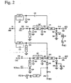
- Fig. 1 shows a high-frequency switch module according to one embodiment of the present invention.
- This high-frequency switch module functions to switch three transmitting and receiving systems, comprising (a) a branching filter circuit comprising first and second filter circuits F1, F2 for dividing a signal introduced into an antenna ANT to a reception signal for the first transmitting and receiving system and a reception signal for the second and third transmitting and receiving systems; (b) a first switch circuit SW1 disposed downstream of the first filter circuit F1 for switching a transmission circuit TX1 and a reception circuit RX1 in the first transmitting and receiving system by voltage applied from a control circuit VC1; (c) a second switch circuit SW2 disposed downstream of the second filter circuit F2 for switching a transmission circuit TX2 in the second and third transmitting and receiving systems, a reception circuit RX2 in the second transmitting and receiving system and a reception circuit RX3 in the third transmitting and receiving system by voltage applied from control circuits VC2, VC3.
- the high-frequency switch module is preferably constituted by an equivalent circuit as shown in Fig. 2.
- the first transmitting and receiving system is GSM (transmission frequency: 880-915 MHz, reception frequency: 925-960 MHz)
- the second transmitting and receiving system is DCS1800 (transmission frequency: 1710-1785 MHz, reception frequency: 1805-1880 MHz)
- the third transmitting and receiving system is PCS (transmission frequency: 1850-1910 MHz, reception frequency: 1930-1990 MHz).
- Each of the first and second filter circuits F1, F2 connected to an antenna ANT is constituted by a distributed constant line and a capacitor.
- the equivalent circuit shown in Fig. 2 comprises a low-pass filter as a first filter circuit F1 for passing transmission and reception signals of GSM while attenuating transmission and reception signals of DCS1800 and PCS, and a high-pass filter as a second filter circuit F2 for passing the transmission and reception signals of DCS1800 and PCS while attenuating the transmission and reception signals of GSM.
- the low-pass filter F1 comprises a distributed constant line LF1, a capacitor CF1 connected in parallel to LF1, and a capacitor CF3 connected between LF1 and CF1 and a ground.
- the high-pass filter F2 comprises a distributed constant line LF2, a capacitor CF2 connected in parallel to LF2, a distributed constant line LF3 connected between LF2 and CF2 and a ground, and a capacitor CF4 connected in series to the distributed constant line LF2 and the capacitor CF2.
- the first and second filter circuits F1, F2 are not restricted to such a structure, permitting the following structures (a) - (h):
- a diode and a distributed constant line are main elements in each of the first switch circuit SW1 disposed downstream of the first and second filter circuits F1, F2 for switching the transmission circuit TX1 and the reception circuit RX1 both for GSM, and the second switch circuit SW2 disposed downstream of the first and second filter circuits F1, F2 for switching the transmission circuit TX2 for DCS1800 and PCS, the reception circuit RX2 for DCS1800, and the reception circuit RX3 for PCS.
- the first switch circuit SW1 is a switch circuit positioning on an upper side in Fig. 2, for switching the transmission circuit TX1 and the reception circuit RX1 for GSM.
- the first switch circuit SW1 comprises two diodes DG1, DG2 and two distributed constant lines LG1, LG2 as main elements.
- the diode DG1 is connected between an input/output terminal IP1, to which an anode of the diode DG1 is connected, and the transmission circuit TX1, and the distributed constant line LG1 is connected to a cathode of the diode DG1 and ground.
- the distributed constant line LG2 is connected between the input/output terminal IP1 and the reception circuit RX1, and the diode DG2 is connected between one end of the distributed constant line LG2 on the side of the reception circuit RX1 and ground. Further, the capacitor CG6 is connected between an anode of the diode DG2 and ground. Connected in series between the above anode and the control circuit VC1 are an inductor LG and a resistor R1.
- Each of the distributed constant lines LG1 and LG2 has a line length in which their resonance frequencies are within a frequency band of the transmission signal of GSM. For instance, when their resonance frequencies are substantially equal to a middle frequency (897.5 MHz) of the transmission signal frequency of GSM, excellent insertion loss characteristics can be obtained within the desired frequency band.
- the low-pass filter circuit LPF inserted between the first filter circuit F1 and the transmission circuit TX1 preferably comprises a distributed constant line and capacitor.
- a ⁇ -type low-pass filter constituted by a distributed constant line LG3 and capacitors CG3, CG4 and CG7 is preferably inserted between the diode DG1 and the distributed constant line LG1.
- the second switch circuit SW2 is a switch circuit positioning on a lower side in Fig. 2, for switching the reception circuit RX2 for DCS1800, the reception circuit RX3 for PCS and the transmission circuit TX2 for DCS1800 and PCS.
- the second switch circuit SW2 comprises three diodes DP1, DP2 and DP3 and two distributed constant lines LP1, LP2 as main elements.
- the diode DP1 is connected between an input/output terminal IP2, to which a cathode of the diode DP1 is connected, and the transmission circuit TX2.
- the distributed constant line LP1 is connected between an anode of the diode DP1 and ground.
- a capacitor CGP is connected between the distributed constant line LP1 and ground, and a control circuit VC3 is connected to one end of the distributed constant line LP1.
- a distributed constant line LP2 is connected between the input/output terminal IP2 and the reception circuit RX2, and an anode of the diode DP2 is connected between one end of the distributed constant line LP2 on the side of the reception circuit RX2 and ground.
- a capacitor CP6 and a resistor R3 are connected in parallel between a cathode of the diode DP2 and ground.
- a diode DP3 is connected between the input/output terminal IP2 and the reception circuit RX3, and an anode of the diode DP3 is connected to a control circuit VC2 via the distributed constant line LP and the resistor R2.
- Each of the distributed constant lines LP1 and LP2 preferably has a line length in which their resonance frequencies are within a range from the maximum frequency to the minimum frequency in a frequency band of the transmission signal of the second and third transmitting and receiving systems, particularly a middle frequency of the maximum frequency and the minimum frequency.
- the resonance frequencies of the distributed constant lines LP1 and LP2 are substantially equal to a middle frequency (1810 MHz) of the transmission signal frequencies of DCS1800 and PCS, excellent electric characteristics can be obtained in respective modes, thereby making it possible to handle two transmission signals in a single circuit.
- a low-pass filter circuit LPF inserted between the second filter circuit F2 and the transmission circuit TX2 is preferably constituted by a distributed constant line and a capacitor.
- a ⁇ -type low-pass filter constituted by a distributed constant line LP3 and capacitors CP3, CP4 and CP7 is preferably inserted between the diode DP1 and the distributed constant line LP1.
- the length of the distributed constant line LP3 is preferably ⁇ /8 to ⁇ /12, wherein ⁇ is a middle frequency of the transmission signal in the second and third transmitting and receiving systems.
- ⁇ is a middle frequency of the transmission signal in the second and third transmitting and receiving systems.
- the middle frequency ⁇ of the transmission signal in the second and third transmitting and receiving systems is equal to a frequency (1810 MHz) intermediate between the transmission signal of DCS1800 (1710-1785 MHz) and the transmission signal of PCS (1850-1910 MHz).
- the distributed constant line LP3 When the distributed constant line LP3 is as long as more than ⁇ /8 relative to the middle frequency ⁇ , the pass band is narrow, failing to obtain the desired insertion loss characteristics at the lowest frequency of the transmission signal of DCS1800 and in the vicinity of the transmission signal of PCS. Also, when the distributed constant line LP3 is as short as less than ⁇ /12, the attenuation of higher frequencies such as double wave, triple wave, etc. is deteriorated. Thus, both cases are not preferable because the high-frequency switch module exhibits deteriorated characteristics.
- the low-pass filter circuit LPF is not restricted to that contained in the switch module as shown in Fig. 1, and may be disposed downstream of the high-frequency switch module as shown in Fig. 16. In this case, the low-pass filter circuit LPF may be composed of a ceramic filter, etc.
- the high-frequency switch module of the present invention selects one of the first, second and third transmitting and receiving systems by controlling the on/off of the diode switches by applying voltage from a power supply means (control circuit).
- a power supply means control circuit
- the distributed constant line LP2 is grounded in a high-frequency manner, resulting in resonance. This leads to extremely large impedance when the second reception circuit RX2 is viewed from the connecting point IP2. Further, with the diode DP3 turned off, there is large impedance between the connecting point IP2 and the third reception circuit RX3. As a result, the transmission signal from the transmission circuit TX2 of the second and third transmitting and receiving systems is transmitted to the second filter circuit F2, without leaking to the second reception circuit RX2 and the third reception circuit RX3.
- the second reception circuit RX2 To connect the second reception circuit RX2 to the second filter circuit F2, zero voltage is applied from the control circuits VC2 and VC3, leaving the diodes DP1, DP2 and DP3 in an OFF state.
- the connecting point IP2 With the diode DP2 in an OFF state, the connecting point IP2 is connected to the second reception circuit RX2 via the distributed constant line LP2.
- the diode DP1 in an OFF state there is large impedance between the connecting point IP2 and the transmission circuit TX2 of the second and third transmitting and receiving systems.
- the diode DP3 With the diode DP3 in an OFF state, there is large impedance between the connecting point IP2 and the third reception circuit RX3.
- the reception signal from the second filter circuit F2 is transmitted to the second reception circuit RX2, without leaking to the transmission circuit TX2 of the second and third transmitting and receiving systems and the third reception circuit RX3.
- the distributed constant line LP2 is grounded in a high-frequency manner, resulting in resonance in a frequency band of the transmission signal for DCS1800 and PCS.
- impedance when the second reception circuit RX2 is viewed from the connecting point IP2 is extremely large in a frequency band of the reception signal for PCS.
- the diode DP1 in an OFF state there is large impedance between the connecting point IP2 and the transmission circuit TX2 of the second and third transmitting and receiving systems.
- the reception signal from the second filter circuit F2 is transmitted to the third reception circuit RX3 without leaking to the transmission circuit TX2 of the second and third transmitting and receiving systems and the second reception circuit RX2.
- the control circuit VC1 To connect the first reception circuit GSM RX to the first filter circuit F1, zero voltage is applied from the control circuit VC1 to turn off the diodes DG1 and DG2. With the diode DG2 in an OFF state, the connecting point IP1 is connected to the first reception circuit RX1 via the distributed constant line LG2. Also, with the diode DG1 in an OFF state, there is large impedance between the connecting point IP1 and the first transmission circuit TX1. As a result, the reception signal from the first filter circuit F1 is transmitted to the first reception circuit RX1 without leaking to the first transmission circuit TX1.
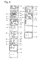
- Fig. 3 is a plan view showing the high-frequency switch module in this EXAMPLE
- Fig. 4 is a perspective view showing a laminate portion thereof
- Fig. 5 is a development view showing the structure of each layer constituting the laminate of Fig. 4.
- the distributed constant lines of the first and second filter circuits, the low-pass filter circuits and the switch circuits are formed in the laminate, while diodes and high-capacitance capacitors as chip capacitors, which cannot be formed in the laminate, are mounted onto the laminate, resulting in a one-chip, triple-band, high-frequency switch module.
- symbols P1 to P16 attached to external terminals in Fig. 4 correspond to symbols such as P2, P4, etc. attached to the equivalent circuit of Fig. 2.
- This laminate can be produced by (a) preparing green sheets of 50-200 ⁇ m in thickness from low-temperature-sinterable dielectric ceramics; (b) printing an electrically conductive, Ag-based paste onto each green sheet to form a desired electrode pattern; (c) integrally laminating a plurality of green sheets having desired electrode patterns; and (d) burning the resultant laminate.
- Line electrodes are preferably as wide as 100-400 ⁇ m.
- a green sheet 11 for the lowermost layer is coated with a ground electrode 31 in substantially all surface and provided with connecting portions for connection to terminal electrodes 81, 83, 87, 91, 93 and 95 on side surfaces.
- a green sheet 13 formed with one line electrode 41, a green sheet 14 formed with four line electrodes 42, 43, 44 and 45, and a green sheet 15 formed with four line electrodes 46, 47, 48 and 49 are laminated in this order thereonto.
- a green sheet 17 formed with a ground electrode 32 is laminated in this order thereonto.
- the line electrodes 41, 42 and 46 connected via through-hole electrodes constitute a distributed constant line LG1
- the line electrodes 45 and 49 connected via through-hole electrodes constitute a distributed constant line LG2
- the line electrodes 43 and 47 connected via through-hole electrodes constitute a distributed constant line LP1
- the line electrodes 44 and 48 connected via through-hole electrodes constitute a distributed constant line LP2.
- Electrodes 61, 62, 63, 64, 65 and 66 for capacitors.
- a green sheet 19 laminated thereon is also formed with electrodes 67, 68 and 69 for capacitors.
- a green sheet 20 laminated thereon is formed with a capacitor electrode 70.
- a green sheet 21 formed with line electrodes 50, 51, 52, 53 and 54, and a green sheet 22 formed with line electrodes 55, 56, 57, 58 and 59 in this order.
- An uppermost green sheet 23 is formed with lands for mounting elements.
- Each of electrodes 61, 62, 63, 64 and 66 for capacitors on the green sheet 18 constitutes capacitance with a ground electrode 32 formed on the green sheet 17.
- the capacitor electrode 61 constitutes a capacitor CP3
- the capacitor electrode 62 constitutes a capacitor CP4
- the capacitor electrode 63 constitutes a capacitor CG4
- the capacitor electrode 64 constitutes a capacitor CG3
- the capacitor electrode 66 constitutes a capacitor CF3.
- Electrodes for capacitors formed on the green sheets 18, 19 and 20 constitute capacitance.
- the capacitor electrodes 65 and 68 constitute a capacitor CF4
- the capacitor electrodes 61 and 62 and 67 constitute a capacitor CP7
- the capacitor electrodes 69 and 70 constitute a capacitor CF1
- the capacitor electrodes 68 and 70 constitute a capacitor CF2.
- the capacitor electrode 65 and the capacitor electrode 68 opposing each other constitute capacitance, though a ground electrode 32 is provided with notches such that these electrodes do not oppose the ground electrode 32.
- Through-hole electrodes for connecting the distributed constant lines are positioned in the notches.
- the line electrodes 52, 59 constitute a distributed constant line LF1; the line electrodes 54, 58 constitute a distributed constant line LF2; the line electrode 53 constitutes a distributed constant line LF3; the line electrodes 51, 57 constitute a distributed constant line LG3; the line electrode 55 constitutes a distributed constant line LP3; and the line electrode 56 constitutes a distributed constant line LP.
- the line electrode 50 functions as a line for wiring. Because the line electrodes 51, 57 constituting the distributed constant line LG3 are formed such that they are partially opposing each other, their opposing portions form a capacitor CG7.
- Laminated green sheets are integrally pressure-bonded and burned at a temperature of 900°C, to provide a laminate of 6.7 mm x 5.0 mm x 1.0 mm in outer size.
- the resultant laminate is formed with terminal electrodes 81-96 on side surfaces. The appearance of the laminate is shown in Fig. 4.
- Fig. 3 is a plan view showing the laminate mounting these elements. Fig. 3 also shows a mounting structure (connection structure of each terminal) of this high-frequency switch module. Incidentally, in Fig. 3, etc., GRD means a terminal connected to a ground.
- CP2, CP5, CG2, CG5, R1, LG, R2 and CP8 in the equivalent circuit shown in Fig. 2 are formed on a circuit mounting chip parts.
- the laminate in this EXAMPLE is formed with terminals on side surfaces, whereby surface mounting can be achieved.
- Terminals mounted onto side surfaces of the laminate are an ANT terminal (P2), a TX2 terminal (P7) for DCS/PCS, a TX1 terminal (P13) for GSM, an RX1 terminal (P16) for GSM, an RX2 terminal (P9) for DCS1800, an RX3 terminal (P10) for PCS, a ground terminal (GRD), and control terminals (VC1, VC2, VC3).
- each side surface of this laminate is provided with at least one ground terminal.
- the ANT terminal, the TX terminals and the RX terminals are respectively sandwiched by ground terminals. Also, VC1, VC2 and VC3 are respectively sandwiched by ground terminals.
- Table 1 shows the control logic of each control circuit VC1, VC2 and VC3 for switching each mode of GSM, DCS1800 and PCS in the high-frequency switch module in this EXAMPLE.
- Table 1 Mode VC1 VC2 VC3 GSM TX High Low Low DCS TX Low Low High PCS TX Low Low High GSM RX Low Low DCS RX Low Low Low PCS RX Low High Low
- Figs. 11-15 show the characteristics of insertion loss and isolation at the time of transmission and reception in each communication mode. As shown in Figs. 11-15, excellent insertion loss characteristics and isolation characteristics were obtained in a desired frequency band in each communication mode, verifying that this EXAMPLE provided a miniaturized, high-performance, high-frequency switch module.
- Fig. 6 shows an equivalent circuit of a high-frequency switch module according to another embodiment of the present invention
- Fig. 7 is a plan view showing the high-frequency switch module
- Fig. 8 shows the internal structure of a laminate for the high-frequency switch module. Because there are many parts common in this EXAMPLE and EXAMPLE 1, explanation will be restricted here to only different parts.
- the first and second filter circuits are the same as those in EXAMPLE 1.
- a first switch circuit SW1 in the first transmitting and receiving system (GSM) is also the same as in EXAMPLE 1, except that a distributed constant line LG1 is connected to a control circuit VC3 together with a distributed constant line LP1 of the second switch circuit SW2 without being connected to a ground electrode.
- the directions of diodes DP1, DP2 and DP3 are opposite to those in EXAMPLE 1, and a control circuit VC4 is connected via a series-connected circuit of an inductor LD and a resistor R3 between the diode DP2 and the capacitor CP6.
- a ground electrode 31 on a green sheet 11 is not connected to a terminal electrode 89.
- a lead terminal of a line electrode 46 is modified.
- a ground electrode 32 is not connected to a terminal electrode 89.
- a line electrode 71, wiring line is added.
- a through-hole for connecting to the line electrode 71 is added.
- the shape of a land is modified.
- Fig. 7 shows a laminate mounted with these elements. Fig. 7 also shows the mounting structure (connecting structure of each terminal) of the high-frequency switch module.
- CP2, CP5, CG2, CG5, R1, LG, R2, CP8, R3 and LD among elements constituting the equivalent circuit of Fig. 6 are mounted onto a chip-part-mounting circuit.
- Table 2 shows the control logic of each control circuit VC1, VC2, VC3 and VC4 for switching each mode in the high-frequency switch module in this EXAMPLE.
- Table 2 Mode VC1 VC2 VC3 VC4 GSM TX High Low Low Low DCS TX Low High Low High PCS TX Low High Low High GSM RX Low Low Low DCS RX Low Low Low Low PCS RX Low Low High High
- the high-frequency switch module of this EXAMPLE can be used in three different communication modes, exhibiting the same effects as in EXAMPLE 1.
- Fig. 9 shows an equivalent circuit of a high-frequency switch module according to another embodiment of the present invention. Because there are many parts common in this EXAMPLE and EXAMPLE 1, explanation will be restricted here to only different parts.
- a second switch circuit SW2 comprises an input/output terminal IP2 for inputting a reception signal for the second and third transmitting and receiving systems from the second filter circuit F2 and outputting a transmission signal from the transmission circuit TX2 of the second and third transmitting and receiving systems; an input terminal for inputting a transmission signal from the transmission circuit TX2 of the second and third transmitting and receiving systems; a third output terminal IP3 for outputting a reception signal of the second and third transmitting and receiving systems; and a fourth output terminal for outputting a reception signal of the second transmitting and receiving system to the reception circuit RX2; a fifth output terminal for outputting a reception signal of the third transmitting and receiving system to the reception circuit RX3; a first diode DP1 connected between the input/output terminal IP2 and the input terminal; a first distributed constant line LP1 connected between the input terminal
- the second switch circuit SW2 comprises a switch circuit SW2-1 for switching the reception circuit RX2 for DCS and the reception circuit RX3 for PCS, and another switch circuit SW2-2 for switching the transmission circuit TX2 and the above switch circuit SW2-1 for DCS/PCS.
- the switch circuit SW2-1 for switching the reception circuit RX2 for DCS and the reception circuit RX3 for PCS comprises two diodes DD1, DD2 and two distributed constant lines LD1, LD2 as main elements, the diode DD2 having an anode connected to a connecting point IP3 and a cathode connected to RX3 and a cathode connected to the distributed constant line LD2 connected to the ground.
- the distributed constant line LD1 is connected between the connecting point IP3 and the reception circuit RX2, and the diode DD1 connected to the ground via the capacitor CDP2 is disposed on the side of the reception circuit RX2.
- a control circuit VC5 is connected between the diode DD1 and the capacitor CDP2 via an inductor LD and a resistor R6.
- This switch circuit SW2-2 Disposed upstream of this switch circuit SW2-1 is another switch circuit SW2-2 for switching the transmission circuit TX2 for DCS/PCS and the switch circuit SW2-1.
- This switch circuit SW2-2 comprises two diodes DP1, DP2 and two distributed constant lines LP1, LP2 as main elements.
- the diode DP1 is connected between TX2 and the connecting point IP2, the diode DP1 having an anode connected to the connecting point IP2 and a cathode connected to the distributed constant line LP1 connected to ground.
- the distributed constant line LP2 is connected between the connecting points IP2 and IP3, and the diode DP2 connected to ground via the capacitor CP6 is disposed on the side of the connecting point IP3.
- Also connected between the diode DP2 and the capacitor CP6 is a control circuit VC3 via an inductor LP and a resistor R3.
- Table 3 shows the control logic of each control circuit VC1, VC3 and VC5 for switching each mode in the high-frequency switch module in this EXAMPLE.
- Table 3 Mode VC1 VC3 VC5 GSM TX High Low Low DCS TX Low High Low PCS TX Low High Low GSM RX Low Low DCS RX Low Low Low PCS RX Low Low High
- the high-frequency switch module of this EXAMPLE can be used in three different communication modes, exhibiting the same effects as in EXAMPLE 1.
- Fig. 10 shows an equivalent circuit of a high-frequency switch module according to a further embodiment of the present invention. Because the high-frequency switch module in this EXAMPLE has many parts common with EXAMPLE 1, explanation will be restricted here to only different parts. First and second switch circuits in the first to third transmitting and receiving systems (GSM, DCS, PCS) are the same as in EXAMPLE 1 with respect to an equivalent circuit.
- the first and second filter circuits F1, F2 connected to an antenna ANT is constituted by a distributed constant line and a capacitor as in EXAMPLE 1, and the equivalent circuit comprises a low-pass filter as a first filter circuit for passing transmission and reception signals for GSM while attenuating transmission and reception signals for DCS and PCS, and a high-pass filter as a second filter circuit for passing transmission and reception signals for DCS and PCS while attenuating transmission and reception signals for GSM.
- the low-pass filter comprises a distributed constant line LF5 between the antenna ANT and the first switch circuit SW1 and a series resonance circuit comprising a distributed constant line LF6 and a capacitor CF6 is connected between one end of the distributed constant line LF5 and ground.
- the high-pass filter comprises a capacitor CF5 connected between the antenna ANT and the second switch circuit SW2, and a series resonance circuit comprising a distributed constant line LF7 and a capacitor CF7, which is connected between CF5 and the ground.
- the high-frequency switch module of this EXAMPLE can be used in three different communication modes, exhibiting the same effects as in EXAMPLE 1.
- the high-frequency switch module of the present invention has been explained in detail referring to Figs. 1-10, it is not restricted thereto, and various modifications may be made unless deviating from the scope of the present invention.
- communication modes usable in the high-frequency switch module of the present invention they are not restricted to combinations shown in EXAMPLES, but switching can be carried out among three different transmitting and receiving systems, for instance, a combination of GPS (Global Positioning System), D-AMPS (Digital Advanced Mobile Service) and PCS, or a combination of GSM, WCDMA (Wide-Band Code Division Multiple Access) and PCS.
- the high-frequency switch module of the present invention can be used, for instance, for portable communications equipment such as triple-band cellular phones of a multi-communication system usable in three different communication systems, it can switch an antenna ANT, a transmission circuit TX1 and a reception circuit RX1 of the first transmitting and receiving system, a transmission circuit TX2 of the second and third transmitting and receiving systems, a reception circuit RX2 of the second transmitting and receiving system, and a reception circuit RX3 of the third transmitting and receiving system, with the transmission circuit of the second transmitting and receiving system and the transmission circuit of the third transmitting and receiving system being made common parts.
- the high-frequency switch module of the present invention can be miniaturized while keeping excellent electric characteristics, with some parts such as amplifiers shared by the second and third transmitting and receiving systems.
- a portable communications equipment comprising the high-frequency switch module can be further miniaturized and reduced in weight.
Description
- The present invention relates to a high-frequency switch module for wireless communications equipment adapted for three different communication modes.
- There are various systems for portable wireless communications equipment, for instance, GSM (Global System for Mobile Communications) and DCS1800 (Digital Cellular System 1800) widely used mostly in Europe, PCS (Personal Communications Services) used in the U. S., and PDC (Personal Digital Cellular) used in Japan. According to recent rapid expansion of cellular phones, however, a frequency band allocated to each system cannot allow all users to use their cellular phones in major cities in advanced countries, resulting in difficulty in connection and thus causing such a problem that cellular phones are disconnected during communication. Thus, proposal was made to permit users to utilize a plurality of systems, thereby increasing substantially usable frequency, and further to expand serviceable territories and to effectively use communications infrastructure of each system.
- However, when the use of a plurality of systems is desired, a user has to carry a necessary number of portable communications equipments corresponding to each system, though there was conventionally no small, light-weight, portable communications equipment capable of communicating by a plurality of systems. What is necessary to enable a single portable communications equipment to use a plurality of systems is to provide the portable communications equipment with parts for each system. High-frequency circuit parts are needed for each system, for instance, a filter for passing a transmission signal of a desired transmission frequency, a high-frequency switch for switching a transmission circuit and a reception circuit and an antenna for emitting a transmission signal and receiving a reception signal in a transmission system; and a filter for passing a signal of a desired frequency among reception signals passing through the high-frequency switch in a reception system. This makes a portable communications equipment unsuitably expensive with increased volume and weight, and to achieve a portable communications equipment capable of using a plurality of systems, the portable communications equipment should have miniaturized, composite-functioning high-frequency circuit parts compatible with frequencies of a plurality of systems.
- Accordingly, an object of the present invention is to provide a miniaturized, high-performance, high-frequency switch module capable of switching transmission circuits and reception circuits of a plurality of systems (particularly three systems) with high-frequency switches, as a high-frequency circuit part used in a portable communications equipment, which permits a single portable communications equipment to be compatible with a plurality of systems.
- EP-A-0 820 155 discloses a duplexer including a high frequency switch, an LC filter serving as a low-pass filter, and an SAW filter serving as a band-pass filter. In contrast to the present invention, the device of this document does not include a second switch circuit connected between the second filter and a transmission circuit.
- EP-A-1 003 291 and EP-A-1 014 592 disclose further relevant HF switch circuits. These two documents have been published after the filing date of the present invention, and belong to the state of the art under Article 54(3) EPC.
- The high-frequency switch module for switching a transmission circuit and a reception circuit in each of a plurality of different transmitting and receiving systems according to the present invention is defined in appended
claim 1. The subclaims relate to preferred embodiments. - In one embodiment of the present invention, the first and second filter circuits function as branching filter circuits for dividing a reception signal for the first transmitting and receiving system and a reception signal for the second and third transmitting and receiving systems.
- The first distributed constant line preferably has a line length in which a resonance frequency thereof is within a range between the maximum frequency and the minimum frequency in a frequency band of the transmission signal for the second and third transmitting and receiving systems. The second distributed constant line preferably has a line length in which a resonance frequency thereof is within a range between the maximum frequency and the minimum frequency in a frequency band of the reception signal for the third transmitting and receiving systems.
- Each of the first and second filter circuits preferably comprises a distributed constant line and a capacitor. At least part of the distributed constant lines and the capacitors in the first and second filter circuits and the distributed constant lines in the first and second switch circuits is preferably constituted by electrode patterns in a laminate comprising dielectric layers having electrode patterns. The diodes in the first and second switch circuits are preferably disposed on the laminate.
- A low-pass filter circuit comprising a distributed constant line and a capacitor is preferably connected between the second filter circuit and the transmission circuit for the second and third transmitting and receiving systems, and at least part of the distributed constant lines and the capacitors are preferably constituted by electrode patterns in the laminate.
- The distributed constant line in the switch circuit is preferably formed by electrode patterns formed in a region sandwiched by as pair of ground electrodes. Capacitors in the first and second filter circuits are preferably formed on a pair of ground electrodes, and distributed constant lines in the first and second filter circuits are preferably formed thereon.
- The distributed constant line in the switch circuit is preferably formed by electrode patterns formed in a region sandwiched by a pair of ground electrodes. Capacitors in the low-pass filter circuit and capacitors in the first and second filter circuits are preferably formed on a ground electrode, and a distributed constant line in the low-pass filter circuit and distributed constant lines in the first and second filter circuits are preferably formed thereon. The first and second filter circuits and the low-pass filter circuit are preferably formed in separate regions not overlapping in a laminating direction of the laminate.
-
- Fig. 1 is a block diagram showing a circuit of a high-frequency switch module according to one embodiment of the present invention;
- Fig. 2 is a schematic view showing an equivalent circuit of the high-frequency switch module according to one embodiment of the present invention;
- Fig. 3 is a plan view showing the high-frequency switch module according to one embodiment of the present invention;
- Fig. 4 is a perspective view showing the high-frequency switch module according to one embodiment of the present invention;
- Fig. 5 is a view showing an internal structure of the high-frequency switch module according to one embodiment of the present invention;
- Fig. 6 is a schematic view showing an equivalent circuit of a high-frequency switch module according to another embodiment of the present invention;
- Fig. 7 is a plan view showing the high-frequency switch module according to another embodiment of the present invention;
- Fig. 8 is a view showing an internal structure of the high-frequency switch module according to another embodiment of the present invention;
- Fig. 9 is a schematic view showing an equivalent circuit of a high-frequency switch module according to a further embodiment of the present invention;
- Fig. 10 is a schematic view showing an equivalent circuit of a high-frequency switch module according to a further embodiment of the present invention;
- Fig. 11(a) is a graph showing the characteristics of insertion loss between TX1 and ANT in a GSM TX mode in the high-frequency switch module in EXAMPLE 1;
- Fig. 11(b) is a graph showing the characteristics of isolation between TX1 and RX1 in a GSM TX mode in the high-frequency switch module in EXAMPLE 1;
- Fig. 12(a) is a graph showing the characteristics of insertion loss between ANT and RX1 in a GSM RX mode in the high-frequency switch module in EXAMPLE 1;
- Fig. 12(b) is a graph showing the characteristics of isolation between ANT and TX1 in a GSM RX mode in the high-frequency switch module in EXAMPLE 1;
- Fig. 13(a) is a graph showing the characteristics of insertion loss between TX2 and ANT in a DCS/PCS TX mode in the high-frequency switch module in EXAMPLE 1;
- Fig. 13(b) is a graph showing the characteristics of isolation between TX2 and RX2 in a DCS/PCS TX mode in the high-frequency switch module in EXAMPLE 1;
- Fig. 13(c) is a graph showing the characteristics of isolation between TX2 and RX3 in a DCS/PCS TX mode in the high-frequency switch module in EXAMPLE 1;
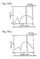
- Fig. 14(a) is a graph showing the characteristics of insertion loss between ANT and RX2 in a DCS RX mode in the high-frequency switch module in EXAMPLE 1;
- Fig. 14(b) is a graph showing the characteristics of isolation between ANT and TX2 in a DCS RX mode in the high-frequency switch module in EXAMPLE 1;
- Fig. 14(c) is a graph showing the characteristics of isolation between ANT and RX3 in a DCS RX mode in the high-frequency switch module in EXAMPLE 1;
- Fig. 15(a) is a graph showing the characteristics of insertion loss between ANT and RX3 in a PCS RX mode in the high-frequency switch module in EXAMPLE 1;
- Fig. 15(b) is a graph showing the characteristics of isolation between ANT and TX2 in a PCS RX mode in the high-frequency switch module in EXAMPLE 1;
- Fig. 15(c) is a graph showing the characteristics of isolation between ANT and RX2 in a PCS RX mode in the high-frequency switch module in EXAMPLE 1; and
- Fig. 16 is a block diagram showing a circuit of a high-frequency switch module according to a further embodiment of the present invention.
- Fig. 1 shows a high-frequency switch module according to one embodiment of the present invention. This high-frequency switch module functions to switch three transmitting and receiving systems, comprising (a) a branching filter circuit comprising first and second filter circuits F1, F2 for dividing a signal introduced into an antenna ANT to a reception signal for the first transmitting and receiving system and a reception signal for the second and third transmitting and receiving systems; (b) a first switch circuit SW1 disposed downstream of the first filter circuit F1 for switching a transmission circuit TX1 and a reception circuit RX1 in the first transmitting and receiving system by voltage applied from a control circuit VC1; (c) a second switch circuit SW2 disposed downstream of the second filter circuit F2 for switching a transmission circuit TX2 in the second and third transmitting and receiving systems, a reception circuit RX2 in the second transmitting and receiving system and a reception circuit RX3 in the third transmitting and receiving system by voltage applied from control circuits VC2, VC3.
- To have the second and third transmitting and receiving systems share a transmission circuit TX2, the high-frequency switch module is preferably constituted by an equivalent circuit as shown in Fig. 2. Explanation will be made below, taking as an example a case where the first transmitting and receiving system is GSM (transmission frequency: 880-915 MHz, reception frequency: 925-960 MHz), the second transmitting and receiving system is DCS1800 (transmission frequency: 1710-1785 MHz, reception frequency: 1805-1880 MHz), and the third transmitting and receiving system is PCS (transmission frequency: 1850-1910 MHz, reception frequency: 1930-1990 MHz).
- Each of the first and second filter circuits F1, F2 connected to an antenna ANT is constituted by a distributed constant line and a capacitor. The equivalent circuit shown in Fig. 2 comprises a low-pass filter as a first filter circuit F1 for passing transmission and reception signals of GSM while attenuating transmission and reception signals of DCS1800 and PCS, and a high-pass filter as a second filter circuit F2 for passing the transmission and reception signals of DCS1800 and PCS while attenuating the transmission and reception signals of GSM.
- The low-pass filter F1 comprises a distributed constant line LF1, a capacitor CF1 connected in parallel to LF1, and a capacitor CF3 connected between LF1 and CF1 and a ground. The high-pass filter F2 comprises a distributed constant line LF2, a capacitor CF2 connected in parallel to LF2, a distributed constant line LF3 connected between LF2 and CF2 and a ground, and a capacitor CF4 connected in series to the distributed constant line LF2 and the capacitor CF2. Incidentally, the first and second filter circuits F1, F2 are not restricted to such a structure, permitting the following structures (a) - (h):
- (a) A structure comprising a low-pass filter as a first filter circuit F1, and a notch filter as a second filter circuit F2;
- (b) A structure comprising a notch filter as a first filter circuit F1, and a band-pass filter as a second filter circuit F2;
- (c) A structure comprising a low-pass filter as a first filter circuit F1, and a band-pass filter as a second filter circuit F2;
- (d) A structure comprising a notch filter as a first filter circuit F1, and a notch filter as a second filter circuit F2;
- (e) A structure comprising a notch filter as a first filter circuit F1, and a high-pass filter as a second filter circuit F2;
- (f) A structure comprising a band-pass filter as a first filter circuit F1, and a band-pass filter as a second filter circuit F2;
- (g) A structure comprising a band-pass filter as a first filter circuit F1, and a notch filter as a second filter circuit F2; and
- (h) A structure comprising a band-pass filter as a first filter circuit F1, and a high-pass filter as a second filter circuit F2.
- A diode and a distributed constant line are main elements in each of the first switch circuit SW1 disposed downstream of the first and second filter circuits F1, F2 for switching the transmission circuit TX1 and the reception circuit RX1 both for GSM, and the second switch circuit SW2 disposed downstream of the first and second filter circuits F1, F2 for switching the transmission circuit TX2 for DCS1800 and PCS, the reception circuit RX2 for DCS1800, and the reception circuit RX3 for PCS.
- The first switch circuit SW1 is a switch circuit positioning on an upper side in Fig. 2, for switching the transmission circuit TX1 and the reception circuit RX1 for GSM. The first switch circuit SW1 comprises two diodes DG1, DG2 and two distributed constant lines LG1, LG2 as main elements. The diode DG1 is connected between an input/output terminal IP1, to which an anode of the diode DG1 is connected, and the transmission circuit TX1, and the distributed constant line LG1 is connected to a cathode of the diode DG1 and ground. The distributed constant line LG2 is connected between the input/output terminal IP1 and the reception circuit RX1, and the diode DG2 is connected between one end of the distributed constant line LG2 on the side of the reception circuit RX1 and ground. Further, the capacitor CG6 is connected between an anode of the diode DG2 and ground. Connected in series between the above anode and the control circuit VC1 are an inductor LG and a resistor R1.
- Each of the distributed constant lines LG1 and LG2 has a line length in which their resonance frequencies are within a frequency band of the transmission signal of GSM. For instance, when their resonance frequencies are substantially equal to a middle frequency (897.5 MHz) of the transmission signal frequency of GSM, excellent insertion loss characteristics can be obtained within the desired frequency band. The low-pass filter circuit LPF inserted between the first filter circuit F1 and the transmission circuit TX1 preferably comprises a distributed constant line and capacitor. In the equivalent circuit shown in Fig. 2, a π-type low-pass filter constituted by a distributed constant line LG3 and capacitors CG3, CG4 and CG7 is preferably inserted between the diode DG1 and the distributed constant line LG1.
- The second switch circuit SW2 is a switch circuit positioning on a lower side in Fig. 2, for switching the reception circuit RX2 for DCS1800, the reception circuit RX3 for PCS and the transmission circuit TX2 for DCS1800 and PCS. The second switch circuit SW2 comprises three diodes DP1, DP2 and DP3 and two distributed constant lines LP1, LP2 as main elements. The diode DP1 is connected between an input/output terminal IP2, to which a cathode of the diode DP1 is connected, and the transmission circuit TX2. The distributed constant line LP1 is connected between an anode of the diode DP1 and ground. A capacitor CGP is connected between the distributed constant line LP1 and ground, and a control circuit VC3 is connected to one end of the distributed constant line LP1.
- A distributed constant line LP2 is connected between the input/output terminal IP2 and the reception circuit RX2, and an anode of the diode DP2 is connected between one end of the distributed constant line LP2 on the side of the reception circuit RX2 and ground. A capacitor CP6 and a resistor R3 are connected in parallel between a cathode of the diode DP2 and ground.
- A diode DP3 is connected between the input/output terminal IP2 and the reception circuit RX3, and an anode of the diode DP3 is connected to a control circuit VC2 via the distributed constant line LP and the resistor R2.
- Each of the distributed constant lines LP1 and LP2 preferably has a line length in which their resonance frequencies are within a range from the maximum frequency to the minimum frequency in a frequency band of the transmission signal of the second and third transmitting and receiving systems, particularly a middle frequency of the maximum frequency and the minimum frequency. For instance, when the resonance frequencies of the distributed constant lines LP1 and LP2 are substantially equal to a middle frequency (1810 MHz) of the transmission signal frequencies of DCS1800 and PCS, excellent electric characteristics can be obtained in respective modes, thereby making it possible to handle two transmission signals in a single circuit.
- A low-pass filter circuit LPF inserted between the second filter circuit F2 and the transmission circuit TX2 is preferably constituted by a distributed constant line and a capacitor. In the equivalent circuit shown in Fig. 2, a π-type low-pass filter constituted by a distributed constant line LP3 and capacitors CP3, CP4 and CP7 is preferably inserted between the diode DP1 and the distributed constant line LP1.
- In the low-pass filter circuit LPF, the length of the distributed constant line LP3 is preferably λ/8 to λ/12, wherein λ is a middle frequency of the transmission signal in the second and third transmitting and receiving systems. For instance, in a case where the second transmitting and receiving system is DCS1800 and the third transmitting and receiving system is PCS, the middle frequency λ of the transmission signal in the second and third transmitting and receiving systems is equal to a frequency (1810 MHz) intermediate between the transmission signal of DCS1800 (1710-1785 MHz) and the transmission signal of PCS (1850-1910 MHz). When the distributed constant line LP3 is as long as more than λ/8 relative to the middle frequency λ, the pass band is narrow, failing to obtain the desired insertion loss characteristics at the lowest frequency of the transmission signal of DCS1800 and in the vicinity of the transmission signal of PCS. Also, when the distributed constant line LP3 is as short as less than λ/12, the attenuation of higher frequencies such as double wave, triple wave, etc. is deteriorated. Thus, both cases are not preferable because the high-frequency switch module exhibits deteriorated characteristics.
- The low-pass filter circuit LPF is not restricted to that contained in the switch module as shown in Fig. 1, and may be disposed downstream of the high-frequency switch module as shown in Fig. 16. In this case, the low-pass filter circuit LPF may be composed of a ceramic filter, etc.
- The high-frequency switch module of the present invention selects one of the first, second and third transmitting and receiving systems by controlling the on/off of the diode switches by applying voltage from a power supply means (control circuit). With respect to the high-frequency switch module shown in Fig. 2, its operation will be explained in detail below.
- To connect the transmission circuit TX2 of the second and third transmitting and receiving systems to the second filter circuit F2, positive voltage is applied from the control circuit VC3, while zero voltage is applied from the control circuit VC2. The positive voltage applied from the control circuit VC3 is deprived of a DC component by capacitors CGP, CP2, CP3, CP4, CP5, CP6 and CF4 and applied to a circuit including diodes DP1, DP2 and DP3. As a result, the diodes DP1, DP2 are turned on, while the diode DP3 is turned off. When the diode DP1 is turned on, impedance becomes low between the transmission circuit TX2 of the second and third transmitting and receiving systems and the connecting point IP2. Also, with the turned-on diode DP2 and the capacitor CP6, the distributed constant line LP2 is grounded in a high-frequency manner, resulting in resonance. This leads to extremely large impedance when the second reception circuit RX2 is viewed from the connecting point IP2. Further, with the diode DP3 turned off, there is large impedance between the connecting point IP2 and the third reception circuit RX3. As a result, the transmission signal from the transmission circuit TX2 of the second and third transmitting and receiving systems is transmitted to the second filter circuit F2, without leaking to the second reception circuit RX2 and the third reception circuit RX3.
- To connect the second reception circuit RX2 to the second filter circuit F2, zero voltage is applied from the control circuits VC2 and VC3, leaving the diodes DP1, DP2 and DP3 in an OFF state. With the diode DP2 in an OFF state, the connecting point IP2 is connected to the second reception circuit RX2 via the distributed constant line LP2. Also, with the diode DP1 in an OFF state, there is large impedance between the connecting point IP2 and the transmission circuit TX2 of the second and third transmitting and receiving systems. Further, with the diode DP3 in an OFF state, there is large impedance between the connecting point IP2 and the third reception circuit RX3. As a result, the reception signal from the second filter circuit F2 is transmitted to the second reception circuit RX2, without leaking to the transmission circuit TX2 of the second and third transmitting and receiving systems and the third reception circuit RX3.
- To connect the third reception circuit RX3 to the second filter circuit F2, positive voltage is applied from the control circuit VC2, and zero voltage is applied from the VC3. Positive voltage applied from the control circuit VC2 is deprived of a DC component by the capacitors CP5, CP6, CP8 and CF4, and applied to a circuit comprising the DP1, DP2 and DP3. As a result, the diodes DP2 and DP3 are turned on, while the diode DP1 is turned off. With the diode DP3 in an ON state, there is small impedance between the third reception circuit RX3 and the connecting point IP2. Also, with the diode DP2 in an ON state and the capacitor CP6, the distributed constant line LP2 is grounded in a high-frequency manner, resulting in resonance in a frequency band of the transmission signal for DCS1800 and PCS. Thus, impedance when the second reception circuit RX2 is viewed from the connecting point IP2 is extremely large in a frequency band of the reception signal for PCS. Further, with the diode DP1 in an OFF state, there is large impedance between the connecting point IP2 and the transmission circuit TX2 of the second and third transmitting and receiving systems. As a result, the reception signal from the second filter circuit F2 is transmitted to the third reception circuit RX3 without leaking to the transmission circuit TX2 of the second and third transmitting and receiving systems and the second reception circuit RX2.
- To connect the first transmission circuit GSM TX to the first filter circuit F1, positive voltage is applied from the control circuit VC1. The positive voltage is deprived of a DC component by the capacitors CG6, CG5, CG4, CG3, CG2 and CG1, and applied to a circuit comprising the diodes DG2 and DG1. As a result, the diodes DG2 and DG1 are turned on. With the diode DG1 in an ON state, there is low impedance between the first transmission circuit TX1 and the connecting point IP1. With the diode DG2 in an ON state and the capacitor CG6, the distributed constant line LG2 is grounded in a high-frequency manner, resulting in resonance. Thus, impedance is extremely large when the first reception circuit RX1 is viewed from the connecting point IP1. As a result, the transmission signal from the first transmission circuit TX1 is transmitted to the first filter circuit F1 without leaking to the reception circuit RX1.
- To connect the first reception circuit GSM RX to the first filter circuit F1, zero voltage is applied from the control circuit VC1 to turn off the diodes DG1 and DG2. With the diode DG2 in an OFF state, the connecting point IP1 is connected to the first reception circuit RX1 via the distributed constant line LG2. Also, with the diode DG1 in an OFF state, there is large impedance between the connecting point IP1 and the first transmission circuit TX1. As a result, the reception signal from the first filter circuit F1 is transmitted to the first reception circuit RX1 without leaking to the first transmission circuit TX1.
- The present invention will be explained in further detail by the following EXAMPLES without intention of restricting the scope of the present invention thereto.
- Fig. 3 is a plan view showing the high-frequency switch module in this EXAMPLE, Fig. 4 is a perspective view showing a laminate portion thereof, and Fig. 5 is a development view showing the structure of each layer constituting the laminate of Fig. 4. In EXAMPLE 1, the distributed constant lines of the first and second filter circuits, the low-pass filter circuits and the switch circuits are formed in the laminate, while diodes and high-capacitance capacitors as chip capacitors, which cannot be formed in the laminate, are mounted onto the laminate, resulting in a one-chip, triple-band, high-frequency switch module. Incidentally, symbols P1 to P16 attached to external terminals in Fig. 4 correspond to symbols such as P2, P4, etc. attached to the equivalent circuit of Fig. 2.
- This laminate can be produced by (a) preparing green sheets of 50-200 µm in thickness from low-temperature-sinterable dielectric ceramics; (b) printing an electrically conductive, Ag-based paste onto each green sheet to form a desired electrode pattern; (c) integrally laminating a plurality of green sheets having desired electrode patterns; and (d) burning the resultant laminate. Line electrodes are preferably as wide as 100-400 µm.
- The internal structure of the laminate will be explained in the order of lamination. First, a
green sheet 11 for the lowermost layer is coated with aground electrode 31 in substantially all surface and provided with connecting portions for connection toterminal electrodes - After laminating a
green sheet 12 with no printed ground onto thegreen sheet 11, agreen sheet 13 formed with oneline electrode 41, agreen sheet 14 formed with fourline electrodes green sheet 15 formed with fourline electrodes green sheet 16 formed with two through-hole electrodes (marked with "+" in the figure), and further laminated thereonto is agreen sheet 17 formed with aground electrode 32. - Proper connection of line electrodes in regions sandwiched by the two
ground electrodes line electrodes line electrodes line electrodes line electrodes - Formed on a
green sheet 18 laminated onto thegreen sheet 17 areelectrodes green sheet 19 laminated thereon is also formed withelectrodes green sheet 20 laminated thereon is formed with acapacitor electrode 70. - Laminated thereon are a
green sheet 21 formed withline electrodes green sheet 22 formed withline electrodes green sheet 23 is formed with lands for mounting elements. - Each of
electrodes green sheet 18 constitutes capacitance with aground electrode 32 formed on thegreen sheet 17. Specifically referring to the equivalent circuit of Fig. 2, thecapacitor electrode 61 constitutes a capacitor CP3, thecapacitor electrode 62 constitutes a capacitor CP4, thecapacitor electrode 63 constitutes a capacitor CG4, thecapacitor electrode 64 constitutes a capacitor CG3, and thecapacitor electrode 66 constitutes a capacitor CF3. - Electrodes for capacitors formed on the
green sheets capacitor electrodes capacitor electrodes capacitor electrodes capacitor electrodes capacitor electrode 65 and thecapacitor electrode 68 opposing each other constitute capacitance, though aground electrode 32 is provided with notches such that these electrodes do not oppose theground electrode 32. Through-hole electrodes for connecting the distributed constant lines are positioned in the notches. - In the
green sheets line electrodes line electrodes line electrode 53 constitutes a distributed constant line LF3; theline electrodes line electrode 55 constitutes a distributed constant line LP3; and theline electrode 56 constitutes a distributed constant line LP. Also, theline electrode 50 functions as a line for wiring. Because theline electrodes - Laminated green sheets are integrally pressure-bonded and burned at a temperature of 900°C, to provide a laminate of 6.7 mm x 5.0 mm x 1.0 mm in outer size. The resultant laminate is formed with terminal electrodes 81-96 on side surfaces. The appearance of the laminate is shown in Fig. 4.
- Mounted onto this laminate are diodes DG1, DG2, DP1, DP2 and DP3, chip capacitors CG1, CG6, CGP and CP6, and a chip resistor R3. Fig. 3 is a plan view showing the laminate mounting these elements. Fig. 3 also shows a mounting structure (connection structure of each terminal) of this high-frequency switch module. Incidentally, in Fig. 3, etc., GRD means a terminal connected to a ground.
- In this EXAMPLE, CP2, CP5, CG2, CG5, R1, LG, R2 and CP8 in the equivalent circuit shown in Fig. 2 are formed on a circuit mounting chip parts.
- In this EXAMPLE, because the distributed constant lines of the first and second switch circuits are formed in regions sandwiched by ground electrodes in the laminate, interference is prevented between the switch circuits, and the branching filter circuit and the low-pass filter circuits. Also, because regions sandwiched by the ground electrodes are disposed in a lower part of the laminate, a ground voltage can easily be obtained. Formed at a position opposing an upper ground electrode is an electrode for constituting a capacitor with the upper ground electrode.
- As shown in Figs. 3 and 4, the laminate in this EXAMPLE is formed with terminals on side surfaces, whereby surface mounting can be achieved. Terminals mounted onto side surfaces of the laminate are an ANT terminal (P2), a TX2 terminal (P7) for DCS/PCS, a TX1 terminal (P13) for GSM, an RX1 terminal (P16) for GSM, an RX2 terminal (P9) for DCS1800, an RX3 terminal (P10) for PCS, a ground terminal (GRD), and control terminals (VC1, VC2, VC3). In addition, each side surface of this laminate is provided with at least one ground terminal.
- In this EXAMPLE, the ANT terminal, the TX terminals and the RX terminals are respectively sandwiched by ground terminals. Also, VC1, VC2 and VC3 are respectively sandwiched by ground terminals.
- Table 1 shows the control logic of each control circuit VC1, VC2 and VC3 for switching each mode of GSM, DCS1800 and PCS in the high-frequency switch module in this EXAMPLE.
Table 1 Mode VC1 VC2 VC3 GSM TX High Low Low DCS TX Low Low High PCS TX Low Low High GSM RX Low Low Low DCS RX Low Low Low PCS RX Low High Low - Figs. 11-15 show the characteristics of insertion loss and isolation at the time of transmission and reception in each communication mode. As shown in Figs. 11-15, excellent insertion loss characteristics and isolation characteristics were obtained in a desired frequency band in each communication mode, verifying that this EXAMPLE provided a miniaturized, high-performance, high-frequency switch module.
- Fig. 6 shows an equivalent circuit of a high-frequency switch module according to another embodiment of the present invention; Fig. 7 is a plan view showing the high-frequency switch module; and Fig. 8 shows the internal structure of a laminate for the high-frequency switch module. Because there are many parts common in this EXAMPLE and EXAMPLE 1, explanation will be restricted here to only different parts.
- The first and second filter circuits are the same as those in EXAMPLE 1. A first switch circuit SW1 in the first transmitting and receiving system (GSM) is also the same as in EXAMPLE 1, except that a distributed constant line LG1 is connected to a control circuit VC3 together with a distributed constant line LP1 of the second switch circuit SW2 without being connected to a ground electrode. In the second switch circuit, the directions of diodes DP1, DP2 and DP3 are opposite to those in EXAMPLE 1, and a control circuit VC4 is connected via a series-connected circuit of an inductor LD and a resistor R3 between the diode DP2 and the capacitor CP6.
- With respect to the structure of the high-frequency switch module, it differs from that of EXAMPLE 1 in the following points. A
ground electrode 31 on agreen sheet 11 is not connected to aterminal electrode 89. In agreen sheet 15, a lead terminal of aline electrode 46 is modified. In agreen sheet 17, aground electrode 32 is not connected to aterminal electrode 89. In agreen sheet 21, aline electrode 71, wiring line, is added. In agreen sheet 22, a through-hole for connecting to theline electrode 71 is added. Also, in agreen sheet 23, the shape of a land is modified. - Mounted onto the laminate are diodes DG1, DG2, DP1, DP2 and DP3 and chip capacitors CG1, CG6, CGP and CP6. Fig. 7 shows a laminate mounted with these elements. Fig. 7 also shows the mounting structure (connecting structure of each terminal) of the high-frequency switch module. In this EXAMPLE, CP2, CP5, CG2, CG5, R1, LG, R2, CP8, R3 and LD among elements constituting the equivalent circuit of Fig. 6 are mounted onto a chip-part-mounting circuit.
- Table 2 shows the control logic of each control circuit VC1, VC2, VC3 and VC4 for switching each mode in the high-frequency switch module in this EXAMPLE.
Table 2 Mode VC1 VC2 VC3 VC4 GSM TX High Low Low Low DCS TX Low High Low High PCS TX Low High Low High GSM RX Low Low Low Low DCS RX Low Low Low Low PCS RX Low Low High High - The high-frequency switch module of this EXAMPLE can be used in three different communication modes, exhibiting the same effects as in EXAMPLE 1.
- Fig. 9 shows an equivalent circuit of a high-frequency switch module according to another embodiment of the present invention. Because there are many parts common in this EXAMPLE and EXAMPLE 1, explanation will be restricted here to only different parts.
- First and second filter circuits and a first switch circuit SW1 in the first transmitting and receiving system (GSM) are the same as in EXAMPLE 1 with respect to an equivalent circuit. A second switch circuit SW2 comprises an input/output terminal IP2 for inputting a reception signal for the second and third transmitting and receiving systems from the second filter circuit F2 and outputting a transmission signal from the transmission circuit TX2 of the second and third transmitting and receiving systems; an input terminal for inputting a transmission signal from the transmission circuit TX2 of the second and third transmitting and receiving systems; a third output terminal IP3 for outputting a reception signal of the second and third transmitting and receiving systems; and a fourth output terminal for outputting a reception signal of the second transmitting and receiving system to the reception circuit RX2; a fifth output terminal for outputting a reception signal of the third transmitting and receiving system to the reception circuit RX3; a first diode DP1 connected between the input/output terminal IP2 and the input terminal; a first distributed constant line LP1 connected between the input terminal and a ground; a second distributed constant line LP2 connected between the input/output terminal IP2 and the third output terminal IP3; a second diode DP2 connected between the third output terminal IP3 and the ground; a third distributed constant line LD1 connected between the third output terminal IP3 and the fourth output terminal; a third diode DD1 connected between the fourth output terminal and the ground; a fourth diode DD2 connected between the third output terminal IP3 and the fifth output terminal; and a fourth distributed constant line LD2 connected between the fifth output terminal and the ground.
- As described above, the second switch circuit SW2 comprises a switch circuit SW2-1 for switching the reception circuit RX2 for DCS and the reception circuit RX3 for PCS, and another switch circuit SW2-2 for switching the transmission circuit TX2 and the above switch circuit SW2-1 for DCS/PCS. The switch circuit SW2-1 for switching the reception circuit RX2 for DCS and the reception circuit RX3 for PCS comprises two diodes DD1, DD2 and two distributed constant lines LD1, LD2 as main elements, the diode DD2 having an anode connected to a connecting point IP3 and a cathode connected to RX3 and a cathode connected to the distributed constant line LD2 connected to the ground. The distributed constant line LD1 is connected between the connecting point IP3 and the reception circuit RX2, and the diode DD1 connected to the ground via the capacitor CDP2 is disposed on the side of the reception circuit RX2. A control circuit VC5 is connected between the diode DD1 and the capacitor CDP2 via an inductor LD and a resistor R6.
- Disposed upstream of this switch circuit SW2-1 is another switch circuit SW2-2 for switching the transmission circuit TX2 for DCS/PCS and the switch circuit SW2-1. This switch circuit SW2-2 comprises two diodes DP1, DP2 and two distributed constant lines LP1, LP2 as main elements. The diode DP1 is connected between TX2 and the connecting point IP2, the diode DP1 having an anode connected to the connecting point IP2 and a cathode connected to the distributed constant line LP1 connected to ground. The distributed constant line LP2 is connected between the connecting points IP2 and IP3, and the diode DP2 connected to ground via the capacitor CP6 is disposed on the side of the connecting point IP3. Also connected between the diode DP2 and the capacitor CP6 is a control circuit VC3 via an inductor LP and a resistor R3.
- Table 3 shows the control logic of each control circuit VC1, VC3 and VC5 for switching each mode in the high-frequency switch module in this EXAMPLE.
Table 3 Mode VC1 VC3 VC5 GSM TX High Low Low DCS TX Low High Low PCS TX Low High Low GSM RX Low Low Low DCS RX Low Low Low PCS RX Low Low High - The high-frequency switch module of this EXAMPLE can be used in three different communication modes, exhibiting the same effects as in EXAMPLE 1.
- Fig. 10 shows an equivalent circuit of a high-frequency switch module according to a further embodiment of the present invention. Because the high-frequency switch module in this EXAMPLE has many parts common with EXAMPLE 1, explanation will be restricted here to only different parts. First and second switch circuits in the first to third transmitting and receiving systems (GSM, DCS, PCS) are the same as in EXAMPLE 1 with respect to an equivalent circuit.
- The first and second filter circuits F1, F2 connected to an antenna ANT is constituted by a distributed constant line and a capacitor as in EXAMPLE 1, and the equivalent circuit comprises a low-pass filter as a first filter circuit for passing transmission and reception signals for GSM while attenuating transmission and reception signals for DCS and PCS, and a high-pass filter as a second filter circuit for passing transmission and reception signals for DCS and PCS while attenuating transmission and reception signals for GSM. The low-pass filter comprises a distributed constant line LF5 between the antenna ANT and the first switch circuit SW1 and a series resonance circuit comprising a distributed constant line LF6 and a capacitor CF6 is connected between one end of the distributed constant line LF5 and ground. On the other hand, the high-pass filter comprises a capacitor CF5 connected between the antenna ANT and the second switch circuit SW2, and a series resonance circuit comprising a distributed constant line LF7 and a capacitor CF7, which is connected between CF5 and the ground.
- The high-frequency switch module of this EXAMPLE can be used in three different communication modes, exhibiting the same effects as in EXAMPLE 1.
- Though the high-frequency switch module of the present invention has been explained in detail referring to Figs. 1-10, it is not restricted thereto, and various modifications may be made unless deviating from the scope of the present invention. With respect to communication modes usable in the high-frequency switch module of the present invention, they are not restricted to combinations shown in EXAMPLES, but switching can be carried out among three different transmitting and receiving systems, for instance, a combination of GPS (Global Positioning System), D-AMPS (Digital Advanced Mobile Service) and PCS, or a combination of GSM, WCDMA (Wide-Band Code Division Multiple Access) and PCS.
- Because the high-frequency switch module of the present invention can be used, for instance, for portable communications equipment such as triple-band cellular phones of a multi-communication system usable in three different communication systems, it can switch an antenna ANT, a transmission circuit TX1 and a reception circuit RX1 of the first transmitting and receiving system, a transmission circuit TX2 of the second and third transmitting and receiving systems, a reception circuit RX2 of the second transmitting and receiving system, and a reception circuit RX3 of the third transmitting and receiving system, with the transmission circuit of the second transmitting and receiving system and the transmission circuit of the third transmitting and receiving system being made common parts. Therefore, the high-frequency switch module of the present invention can be miniaturized while keeping excellent electric characteristics, with some parts such as amplifiers shared by the second and third transmitting and receiving systems. As a result, a portable communications equipment comprising the high-frequency switch module can be further miniaturized and reduced in weight.
Claims (5)
- A high-frequency switch module for switching transmission circuits and reception circuits in different transmitting and receiving systems (GSM, DCS, PCS), comprising first and second filter circuits (F1, F2) having different pass bands, wherein
said first filter circuit (F1) is connected between an antenna (ANT) and a first switch circuit (SW1),
said second filter circuit (F2) is connected between said antenna (ANT) and a second switch circuit (SW2),
said first switch circuit (SW1) is connected to said first filter circuit (F1) for switching a first transmission circuit (TX1) and a first reception circuit (RX1) in a first transmitting and receiving system (GSM), and
said second switch circuit (SW2) is connected to said second filter circuit (F2) for switching a second transmission circuit (TX2) of second and third transmitting and receiving systems (DCS, PCS), a second reception circuit (RX2) of said second transmitting and receiving system (DCS) and a third reception circuit (RX3) of said third transmitting and receiving system (PCS), and
each of said first and second switch circuits (SW1, SW2) is a diode switch comprising a diode (DG1, DG2; DP1, DP2, DP3; DP1, DP2, DD1, DD2) and a distributed constant line (LG2; LP2; LP2, LD1), whereby one of said first, second and third transmitting and receiving systems (GSM, DCS, PCS) is selected by controlling the on/off of said diode switches by applying voltage from a power supply means to said diode switches,
said second switch circuit (SW2) comprises:a first diode (DP1) connected between said second transmission circuit (TX2) and said second filter circuit (F2), said second filter circuit (F2) comprising a distributed constant line (LF2; LF7) and a capacitor (CF2; CF5);a first distributed constant line (LP2), whose one side is connected to said second filter circuit (F2);a second diode (DP2) connected to ground at the other side of said first distributed constant line (LP2);a capacitor (CP5) connected in series to said first distributed constant line (LP2);a third diode (DD2) connected between said capacitor (CP5) and said third reception circuit (RX3); anda second distributed constant line (LD1) connected between said capacitor (CP5) and said second reception circuit (RX2), andsaid third diode (DD2) is connected to ground through said second distributed constant line (LD1) and a fourth diode (DD1). - The module of claim 1, wherein
said first switch circuit (SW1) comprises:a first diode (DG1) connected between said first transmission circuit (TX1) and said first filter circuit (F2), said first filter circuit (F1) comprising a distributed constant line (LF1) and a capacitor (CF1); anda distributed constant line (LG2) connected between said first filter circuit (F1) and said first reception circuit (RX1), andsaid first diode (DG1) is connected to ground through said distributed constant line (LG2) and a second diode (DG2). - The module of claim 1 or 2, wherein a low-pass filter (LPF) comprising a distributed constant line (LP3) and a capacitor (CP3, CP4, CP7) is connected between said second filter circuit (F2) and said second transmission circuit (TX2).
- The module of claim 3, wherein the line length of said distributed constant line constituting said low-pass filter (LPF) is λ/8 to λ/12, wherein λ is a middle frequency of said transmission signal for said second and third transmitting and receiving systems.
- The module of any preceding claim, wherein each of said first and second filter circuits (F1, F2) comprises a distributed constant line (LF1; LF2, LF3 or LF5, LF6; LF7) and a capacitor (CF1, CF3; CF2, CF4 or CF6; CF5, CF7).
Priority Applications (2)
| Application Number | Priority Date | Filing Date | Title |
|---|---|---|---|
| EP07005601A EP1804390B1 (en) | 1999-03-18 | 2000-03-17 | High frequency switch module |
| EP07005602A EP1801990A1 (en) | 1999-03-18 | 2000-03-17 | High frequency switch |
Applications Claiming Priority (3)
| Application Number | Priority Date | Filing Date | Title |
|---|---|---|---|
| JP7323499 | 1999-03-18 | ||
| JP07323499A JP2002064301A (en) | 1999-03-18 | 1999-03-18 | High frequency switch module for triple band |
| PCT/JP2000/001670 WO2000055983A1 (en) | 1999-03-18 | 2000-03-17 | High-frequency switch module |
Related Child Applications (2)
| Application Number | Title | Priority Date | Filing Date |
|---|---|---|---|
| EP07005601A Division EP1804390B1 (en) | 1999-03-18 | 2000-03-17 | High frequency switch module |
| EP07005602A Division EP1801990A1 (en) | 1999-03-18 | 2000-03-17 | High frequency switch |
Publications (3)
| Publication Number | Publication Date |
|---|---|
| EP1083672A1 EP1083672A1 (en) | 2001-03-14 |
| EP1083672A4 EP1083672A4 (en) | 2004-06-23 |
| EP1083672B1 true EP1083672B1 (en) | 2007-05-09 |
Family
ID=13512301
Family Applications (3)
| Application Number | Title | Priority Date | Filing Date |
|---|---|---|---|
| EP07005602A Withdrawn EP1801990A1 (en) | 1999-03-18 | 2000-03-17 | High frequency switch |
| EP00909731A Expired - Lifetime EP1083672B1 (en) | 1999-03-18 | 2000-03-17 | High-frequency switch module |
| EP07005601A Expired - Lifetime EP1804390B1 (en) | 1999-03-18 | 2000-03-17 | High frequency switch module |
Family Applications Before (1)
| Application Number | Title | Priority Date | Filing Date |
|---|---|---|---|
| EP07005602A Withdrawn EP1801990A1 (en) | 1999-03-18 | 2000-03-17 | High frequency switch |
Family Applications After (1)
| Application Number | Title | Priority Date | Filing Date |
|---|---|---|---|
| EP07005601A Expired - Lifetime EP1804390B1 (en) | 1999-03-18 | 2000-03-17 | High frequency switch module |
Country Status (6)
| Country | Link |
|---|---|
| US (3) | US6987984B1 (en) |
| EP (3) | EP1801990A1 (en) |
| JP (2) | JP2002064301A (en) |
| DE (1) | DE60034747T2 (en) |
| DK (1) | DK1083672T3 (en) |
| WO (1) | WO2000055983A1 (en) |
Families Citing this family (47)
| Publication number | Priority date | Publication date | Assignee | Title |
|---|---|---|---|---|
| US7395056B2 (en) * | 2000-05-31 | 2008-07-01 | Wahoo Communications Corporation | Time-shared full duplex protocol for use with a wireless communications system with artificial intelligence-based distributive call routing |
| EP1313227B1 (en) * | 2000-08-22 | 2011-06-15 | Hitachi Metals, Ltd. | Laminated high-frequency switch module |
| EP1333588B1 (en) | 2000-11-01 | 2012-02-01 | Hitachi Metals, Ltd. | High-frequency switch module |
| EP1223634A3 (en) * | 2000-12-26 | 2003-08-13 | Matsushita Electric Industrial Co., Ltd. | High-frequency switch, laminated high-frequency switch, high-frequency radio unit, and high-frequency switching method |
| DE10102201C2 (en) * | 2001-01-18 | 2003-05-08 | Epcos Ag | Electrical switching module, switching module arrangement and use of the switching module and the switching module arrangement |
| FR2822612B1 (en) * | 2001-03-20 | 2003-07-11 | Sagem | RADIO FREQUENCY MULTIPLEXING DEVICE WITH CROSS CONTROL FOR TWO-BAND MOBILE TELEPHONE |
| JP2002290269A (en) * | 2001-03-27 | 2002-10-04 | Sanyo Electric Co Ltd | Hybrid high frequency component and information terminal employing it |
| EP1374426B1 (en) * | 2001-03-29 | 2006-01-11 | Matsushita Electric Industrial Co., Ltd. | High frequency switch, radio communication apparatus, and high frequency switching method |
| US6683512B2 (en) * | 2001-06-21 | 2004-01-27 | Kyocera Corporation | High frequency module having a laminate board with a plurality of dielectric layers |
| US6865376B2 (en) * | 2001-07-03 | 2005-03-08 | Kyocera Wireless Corp. | System and method for a GPS enabled antenna |
| US7057472B2 (en) | 2001-08-10 | 2006-06-06 | Hitachi Metals, Ltd. | Bypass filter, multi-band antenna switch circuit, and layered module composite part and communication device using them |
| JP2003087002A (en) * | 2001-09-14 | 2003-03-20 | Matsushita Electric Ind Co Ltd | High-frequency switch |
| US7492565B2 (en) * | 2001-09-28 | 2009-02-17 | Epcos Ag | Bandpass filter electrostatic discharge protection device |
| US20050059371A1 (en) * | 2001-09-28 | 2005-03-17 | Christian Block | Circuit arrangement, switching module comprising said circuit arrangement and use of switching module |
| CN1494771A (en) | 2001-10-24 | 2004-05-05 | ���µ�����ҵ��ʽ���� | High-frequency composite switch module and communication terminal using it |
| US6975841B2 (en) | 2001-11-12 | 2005-12-13 | Matsushita Electric Industrial Co., Ltd. | Diplexer, and high-frequency switch and antenna duplexer using the same |
| US7167687B2 (en) | 2002-01-31 | 2007-01-23 | Hitachi Metals, Ltd. | Switch circuit and composite high-frequency part |
| JP2003264348A (en) * | 2002-03-07 | 2003-09-19 | Sony Corp | High frequency module |
| JP2003338701A (en) | 2002-05-20 | 2003-11-28 | Seiko Epson Corp | Manufacturing method for high-frequency switch, the high-frequency switch and electronic device |
| DE10246098A1 (en) | 2002-10-02 | 2004-04-22 | Epcos Ag | circuitry |
| WO2004038913A1 (en) * | 2002-10-25 | 2004-05-06 | Hitachi Metals, Ltd. | Balanced-unblanced type multi-band filer module |
| US20040185795A1 (en) * | 2003-02-05 | 2004-09-23 | Khosro Shamsaifar | Electronically tunable RF Front End Module |
| JP3761000B2 (en) | 2003-02-14 | 2006-03-29 | 日立金属株式会社 | Switch circuit and composite high-frequency components |
| US7373171B2 (en) * | 2003-02-14 | 2008-05-13 | Tdk Corporation | Front end module |
| JP3810011B2 (en) * | 2003-08-08 | 2006-08-16 | Tdk株式会社 | High frequency switch module and multilayer substrate for high frequency switch module |
| JP4123435B2 (en) * | 2003-10-14 | 2008-07-23 | 富士通メディアデバイス株式会社 | High frequency switch module |
| WO2005046070A1 (en) * | 2003-11-11 | 2005-05-19 | Murata Manufacturing Co., Ltd. | High frequency module |
| WO2005122417A1 (en) | 2004-06-07 | 2005-12-22 | Hitachi Metals, Ltd. | High frequency switch module and method for controlling the same |
| JP4288529B2 (en) * | 2004-06-30 | 2009-07-01 | 日立金属株式会社 | High frequency components and multiband communication devices |
| WO2006003959A1 (en) * | 2004-06-30 | 2006-01-12 | Hitachi Metals, Ltd. | High frequency circuit, high frequency component, and multi-band communication apparatus |
| DE102004040967B4 (en) * | 2004-08-24 | 2019-02-21 | Snaptrack, Inc. | High isolation circuit between transmit and receive paths and device with the circuit |
| KR100845491B1 (en) | 2004-11-25 | 2008-07-10 | 가부시키가이샤 무라타 세이사쿠쇼 | High frequency switch module |
| JP4552193B2 (en) * | 2005-02-24 | 2010-09-29 | 日立金属株式会社 | Multiband high frequency module and multiband communication apparatus using the same |
| EP1876722B1 (en) * | 2005-04-28 | 2016-08-24 | Murata Manufacturing Co., Ltd. | High frequency switching module and method for adjusting frequency characteristic of high frequency circuit |
| US7564664B2 (en) * | 2006-05-11 | 2009-07-21 | Infineon Technologies Ag | ESD protection circuit for a high frequency circuit |
| ATE437478T1 (en) * | 2007-05-22 | 2009-08-15 | Alcatel Lucent | BASE STATION AND TRANSMISSION METHOD |
| US7702296B2 (en) * | 2007-08-01 | 2010-04-20 | Mediatek Usa Inc. | Transmit/receive switch |
| JP4873046B2 (en) * | 2009-05-26 | 2012-02-08 | 株式会社村田製作所 | High frequency module |
| JP5625453B2 (en) | 2009-05-26 | 2014-11-19 | 株式会社村田製作所 | High frequency switch module |
| TWI408910B (en) * | 2009-10-14 | 2013-09-11 | Ralink Technology Corp | Signal splitting device and wireless communication device using the same |
| US9100060B2 (en) * | 2011-12-14 | 2015-08-04 | Infineon Technologies Ag | System and method for a radio frequency switch |
| JP5594318B2 (en) | 2012-05-24 | 2014-09-24 | 株式会社村田製作所 | Switch module |
| US11063570B2 (en) | 2017-02-10 | 2021-07-13 | Telefonaktiebolaget Lm Ericsson (Publ) | Integrated isolator circuit in a time division duplex transceiver |
| JP2021145282A (en) * | 2020-03-13 | 2021-09-24 | 株式会社村田製作所 | High frequency module and communication device |
| JP2021158556A (en) * | 2020-03-27 | 2021-10-07 | 株式会社村田製作所 | High-frequency module and communication device |
| JP2021158554A (en) * | 2020-03-27 | 2021-10-07 | 株式会社村田製作所 | High-frequency module and communication device |
| CN114257265B (en) * | 2022-03-01 | 2022-05-10 | 四川鸿创电子科技有限公司 | Radio frequency to intermediate frequency receiving and transmitting system |
Family Cites Families (31)
| Publication number | Priority date | Publication date | Assignee | Title |
|---|---|---|---|---|
| DE4222190A1 (en) * | 1992-07-07 | 1994-01-13 | Philips Patentverwaltung | Radio with an antenna switching device |
| US5442812A (en) * | 1992-07-08 | 1995-08-15 | Matsushita Electric Industrial Co., Ltd. | Antenna switching apparatus for selectively connecting antenna to transmitter or receiver |
| DE4343719C2 (en) * | 1992-12-22 | 1997-08-07 | Murata Manufacturing Co | High frequency switch |
| JP2874496B2 (en) | 1992-12-26 | 1999-03-24 | 株式会社村田製作所 | High frequency switch |
| CA2135799A1 (en) * | 1993-03-31 | 1994-10-13 | Darioush Agahi-Kesheh | Switch circuit and method therefor |
| JP3291913B2 (en) * | 1994-05-17 | 2002-06-17 | 株式会社村田製作所 | High frequency switch |
| JP3198808B2 (en) * | 1994-06-30 | 2001-08-13 | 株式会社村田製作所 | High frequency switch |
| JP3196539B2 (en) * | 1994-12-05 | 2001-08-06 | 株式会社村田製作所 | High frequency switch |
| JP3299065B2 (en) * | 1995-01-30 | 2002-07-08 | 株式会社村田製作所 | High frequency composite switch |
| DE69612041T2 (en) * | 1995-07-24 | 2001-08-02 | Murata Manufacturing Co | High frequency switch |
| US5999065A (en) * | 1995-08-24 | 1999-12-07 | Murata Manufacturing Co., Ltd. | Composite high-frequency component |
| US6070059A (en) * | 1995-12-05 | 2000-05-30 | Murata Manufacturing Co., Ltd. | High-frequency switch |
| US5742212A (en) * | 1995-12-05 | 1998-04-21 | Murata Manufacturing Co., Ltd. | High-frequency switch |
| JPH1032521A (en) | 1996-07-17 | 1998-02-03 | Murata Mfg Co Ltd | Duplexer |
| US6006105A (en) * | 1996-08-02 | 1999-12-21 | Lsi Logic Corporation | Multi-frequency multi-protocol wireless communication device |
| US5768691A (en) * | 1996-08-07 | 1998-06-16 | Nokia Mobile Phones Limited | Antenna switching circuits for radio telephones |
| JP3223848B2 (en) * | 1996-08-21 | 2001-10-29 | 株式会社村田製作所 | High frequency components |
| JPH10135702A (en) * | 1996-10-29 | 1998-05-22 | Hitachi Metals Ltd | Diode switch |
| US5778306A (en) * | 1996-11-08 | 1998-07-07 | Motorola Inc. | Low loss high frequency transmitting/receiving switching module |
| JP3258922B2 (en) * | 1997-01-08 | 2002-02-18 | 三洋電機株式会社 | Dual band wireless communication device |
| US6108527A (en) * | 1997-07-31 | 2000-08-22 | Lucent Technologies, Inc. | Wide range multiple band RF power detector |
| JP3848445B2 (en) | 1997-09-26 | 2006-11-22 | 松下電器産業株式会社 | Radio equipment compatible with multiple communication systems |
| ES2232909T3 (en) * | 1997-12-03 | 2005-06-01 | Hitachi Metals, Ltd. | HIGH FREQUENCY MULTIBAND SWITCH MODULE. |
| JP3191213B2 (en) | 1998-04-28 | 2001-07-23 | 日立金属株式会社 | High frequency switch module |
| JP2983016B2 (en) | 1997-12-03 | 1999-11-29 | 日立金属株式会社 | High frequency switch module for multi-band |
| JP3304901B2 (en) * | 1998-11-27 | 2002-07-22 | 株式会社村田製作所 | Composite high frequency component and mobile communication device using the same |
| DE69941583D1 (en) * | 1998-10-27 | 2009-12-03 | Murata Manufacturing Co | Composite high frequency component and mobile communication device equipped therewith |
| JP3304898B2 (en) | 1998-11-20 | 2002-07-22 | 株式会社村田製作所 | Composite high frequency component and mobile communication device using the same |
| JP3484090B2 (en) * | 1998-12-22 | 2004-01-06 | 株式会社日立製作所 | Switched antenna duplexer and mobile radio terminal |
| JP2001102957A (en) * | 1999-09-28 | 2001-04-13 | Murata Mfg Co Ltd | Composite high-frequency component and mobile communication device using same |
| JP3711846B2 (en) * | 2000-07-27 | 2005-11-02 | 株式会社村田製作所 | High frequency module and mobile communication device using the same |
-
1999
- 1999-03-18 JP JP07323499A patent/JP2002064301A/en active Pending
-
2000
- 2000-03-17 EP EP07005602A patent/EP1801990A1/en not_active Withdrawn
- 2000-03-17 EP EP00909731A patent/EP1083672B1/en not_active Expired - Lifetime
- 2000-03-17 EP EP07005601A patent/EP1804390B1/en not_active Expired - Lifetime
- 2000-03-17 DE DE60034747T patent/DE60034747T2/en not_active Expired - Lifetime
- 2000-03-17 JP JP2000605318A patent/JP4257481B2/en not_active Expired - Fee Related
- 2000-03-17 WO PCT/JP2000/001670 patent/WO2000055983A1/en active IP Right Grant
- 2000-03-17 DK DK00909731T patent/DK1083672T3/en active
- 2000-03-17 US US09/700,671 patent/US6987984B1/en not_active Expired - Lifetime
-
2005
- 2005-03-28 US US11/090,640 patent/US7171234B2/en not_active Expired - Lifetime
- 2005-03-28 US US11/090,218 patent/US7130655B2/en not_active Expired - Lifetime
Also Published As
| Publication number | Publication date |
|---|---|
| WO2000055983A1 (en) | 2000-09-21 |
| EP1801990A1 (en) | 2007-06-27 |
| US20050221768A1 (en) | 2005-10-06 |
| EP1804390B1 (en) | 2011-05-11 |
| EP1083672A4 (en) | 2004-06-23 |
| DK1083672T3 (en) | 2007-08-06 |
| EP1804390A1 (en) | 2007-07-04 |
| JP4257481B2 (en) | 2009-04-22 |
| US20050221769A1 (en) | 2005-10-06 |
| US6987984B1 (en) | 2006-01-17 |
| JP2002064301A (en) | 2002-02-28 |
| US7130655B2 (en) | 2006-10-31 |
| EP1083672A1 (en) | 2001-03-14 |
| US7171234B2 (en) | 2007-01-30 |
| DE60034747T2 (en) | 2008-01-17 |
| DE60034747D1 (en) | 2007-06-21 |
Similar Documents
| Publication | Publication Date | Title |
|---|---|---|
| EP1083672B1 (en) | High-frequency switch module | |
| EP1313227B1 (en) | Laminated high-frequency switch module | |
| EP1168650B1 (en) | High-frequency switch, high-frequency switch module, and wireless communication device | |
| KR100757915B1 (en) | High-frequency switch module | |
| EP2197120A2 (en) | High-frequency module and wireless communication device | |
| JP3191213B2 (en) | High frequency switch module | |
| JP3874237B2 (en) | Low distortion high frequency switch module | |
| JP3642062B2 (en) | High frequency switch | |
| JP4210861B2 (en) | High frequency switch module | |
| JP2004007585A (en) | High frequency switch module for multiband | |
| JP2004007756A5 (en) | ||
| JP4174779B2 (en) | High frequency switch module | |
| JP4135015B2 (en) | High frequency switch module | |
| JP3550668B2 (en) | High frequency switch module | |
| JP2006203946A (en) | High-frequency switch module | |
| JP2002300051A (en) | High frequency module | |
| JP2005237019A (en) | High frequency switch |
Legal Events
| Date | Code | Title | Description |
|---|---|---|---|
| PUAI | Public reference made under article 153(3) epc to a published international application that has entered the european phase |
Free format text: ORIGINAL CODE: 0009012 |
|
| 17P | Request for examination filed |
Effective date: 20001218 |
|
| AK | Designated contracting states |
Kind code of ref document: A1 Designated state(s): AT BE CH CY DE DK ES FI FR GB GR IE IT LI LU MC NL PT SE |
|
| RBV | Designated contracting states (corrected) |
Designated state(s): DE DK FI FR GB |
|
| A4 | Supplementary search report drawn up and despatched |
Effective date: 20040511 |
|
| 17Q | First examination report despatched |
Effective date: 20041014 |
|
| 17Q | First examination report despatched |
Effective date: 20041014 |
|
| GRAP | Despatch of communication of intention to grant a patent |
Free format text: ORIGINAL CODE: EPIDOSNIGR1 |
|
| GRAS | Grant fee paid |
Free format text: ORIGINAL CODE: EPIDOSNIGR3 |
|
| GRAA | (expected) grant |
Free format text: ORIGINAL CODE: 0009210 |
|
| AK | Designated contracting states |
Kind code of ref document: B1 Designated state(s): DE DK FI FR GB |
|
| REG | Reference to a national code |
Ref country code: GB Ref legal event code: FG4D |
|
| REF | Corresponds to: |
Ref document number: 60034747 Country of ref document: DE Date of ref document: 20070621 Kind code of ref document: P |
|
| REG | Reference to a national code |
Ref country code: DK Ref legal event code: T3 |
|
| ET | Fr: translation filed | ||
| PLBE | No opposition filed within time limit |
Free format text: ORIGINAL CODE: 0009261 |
|
| STAA | Information on the status of an ep patent application or granted ep patent |
Free format text: STATUS: NO OPPOSITION FILED WITHIN TIME LIMIT |
|
| 26N | No opposition filed |
Effective date: 20080212 |
|
| REG | Reference to a national code |
Ref country code: GB Ref legal event code: 732E |
|
| REG | Reference to a national code |
Ref country code: FR Ref legal event code: TP |
|
| PGFP | Annual fee paid to national office [announced via postgrant information from national office to epo] |
Ref country code: DK Payment date: 20120312 Year of fee payment: 13 Ref country code: FI Payment date: 20120312 Year of fee payment: 13 |
|
| REG | Reference to a national code |
Effective date: 20130331 Ref country code: DK Ref legal event code: EBP |
|
| PG25 | Lapsed in a contracting state [announced via postgrant information from national office to epo] |
Ref country code: FI Free format text: LAPSE BECAUSE OF NON-PAYMENT OF DUE FEES Effective date: 20130317 |
|
| PG25 | Lapsed in a contracting state [announced via postgrant information from national office to epo] |
Ref country code: DK Free format text: LAPSE BECAUSE OF NON-PAYMENT OF DUE FEES Effective date: 20130331 |
|
| REG | Reference to a national code |
Ref country code: FR Ref legal event code: PLFP Year of fee payment: 17 |
|
| REG | Reference to a national code |
Ref country code: FR Ref legal event code: PLFP Year of fee payment: 18 |
|
| REG | Reference to a national code |
Ref country code: FR Ref legal event code: PLFP Year of fee payment: 19 |
|
| PGFP | Annual fee paid to national office [announced via postgrant information from national office to epo] |
Ref country code: GB Payment date: 20190313 Year of fee payment: 20 Ref country code: DE Payment date: 20190305 Year of fee payment: 20 |
|
| PGFP | Annual fee paid to national office [announced via postgrant information from national office to epo] |
Ref country code: FR Payment date: 20190213 Year of fee payment: 20 |
|
| REG | Reference to a national code |
Ref country code: DE Ref legal event code: R071 Ref document number: 60034747 Country of ref document: DE |
|
| REG | Reference to a national code |
Ref country code: GB Ref legal event code: PE20 Expiry date: 20200316 |
|
| PG25 | Lapsed in a contracting state [announced via postgrant information from national office to epo] |
Ref country code: GB Free format text: LAPSE BECAUSE OF EXPIRATION OF PROTECTION Effective date: 20200316 |