FIELD OF THE INVENTION
The present invention relates generally to an
electrodeposited copper foil with its surface prepared
wherein a matte side, namely a surface at which copper
deposition is completed, is mechanically polished at
least once and the thus mechanically polished matte
side is subjected to a selective chemical polishing so
as to attain preparing thereof, and relates to a
process for producing the same and a use of the
electrodeposited copper foil with its surface prepared
in, for example, a printed wiring board.
BACKGROUND OF THE INVENTION
In recent years, both the size and weight of
electronic equipment such as a notebook-sized personal
computer are being reduced to increasing extents.
Accordingly, IC wiring is also becoming finer.
With respect to the wiring pattern formed on a
substrate used in such an electronic equipment, the
lead width is now as small as ten-odd microns (µm). In
accordance therewith, the metal foil constituting the
wiring pattern is becoming thinner. Specifically,
while the designated thickness of metal foil for use in
the formation of the conventional wiring pattern of
about 100 µm lead width has ranged from about 15 to 35
µm in correspondence to the width of the wiring pattern,
the thickness of metal foil employed in the formation
of ten-odd micron (µm) wiring pattern must be reduced
in correspondence thereto.
For example, an aluminum foil or a copper foil is
used as the metal foil for constituting the above
wiring pattern. It is preferred to employ a copper
foil, especially an electrodeposited copper foil, as
the metal foil.
The electrodeposited copper foil employed for
forming the above wiring pattern is produced by
electrodepositing copper on a drum surface. With
respect to the thus produced electrodeposited copper
foil, the surface at which copper deposition is
initiated, namely the surface at which formation of
copper deposits brought into contact with the drum is
initiated, is referred to as "shiny side", and the
surface at which copper deposition is completed is
referred to as "matte side". The surface condition of
the shiny side is substantially the same as that of the
drum. That is, the 10-point average surface roughness
(Rz) in ISO 4287 of the drum is about from 1.2 to 2.5
µm, to which the 10-point average surface roughness
(Rz) of the shiny side is nearly equal. On the other
hand, with respect to the matte side, its surface
roughness is greater than the surface roughness of the
shiny side, and the 10-point average surface roughness
of the matte side, although varied depending on the
deposition condition of copper and the thickness
thereof, is generally in the range of about 2.5 to 10
µm. In the conventional electrodeposited copper foil
of about 35 µm nominal thickness, it has been rare that
the surface roughness of the matte side poses a problem.
However, in the electrodeposited copper foil of ten-odd
micron (µm) thickness, the surface roughness of the
matte side is equivalent to tens of percents of the
thickness of the whole electrodeposited copper foil,
and the condition of the matte side exerts marked
influence on the electrical properties of formed wiring
pattern and board per se. It is known that, for
example, mechanical polishing, chemical polishing and
electrolytic polishing are available as the means for
preparing the state of surface of the copper foil. The
mechanical polishing is a method of smoothing the
surface of the copper foil with the use of, for example,
a buff. When use is made of a thin copper foil, the
copper foil may be broken by mechanical stress exerted
on the copper foil. Thus, the mechanical polishing is
suitable for the preparing of the surface of relatively
thick copper foils. On the other hand, no mechanical
stress is exerted on the copper foil in the chemical
polishing and electrolytic polishing, as different from
the mechanical polishing, so that even thin copper
foils would not be broken by the chemical polishing and
electrolytic polishing. Thus, it has been believed
that the chemical polishing and electrolytic polishing
are suitable for the preparing of the surface of
relatively thin copper foils.
For example, Japanese Patent Unexamined
Publication No. Hei 5-160208 discloses a tape carrier
having a lead pattern formed from an electrodeposited
copper foil wherein the overall surface of matte side
obtained by electrodeposition has been polished. This
publication discloses the use, in the formation of a
lead pattern of 60 to 80 µm pitch, of an
electrodeposited copper foil whose 1-2 µm of matte side
surface profile has been chemically polished to thereby
attain preparing of the matte side. The thickness of
the there employed electrodeposited copper foil after
the preparing is in the range of 18 to 30 µm. It is
disclosed that a highly reliable carrier tape with
desired lead strength can be provided by the use of the
copper foil whose matte side overall surface has been
chemically polished.
However, the preparing of copper foil by chemical
polishing as described in the above publication,
although protrudent parts of the matte side are leached
with relatively high selectivity to thereby effect
preparing thereof, also invites leaching of the copper
constituting the depressed parts of the matte side.
Therefore, in this chemical polishing, the whole copper
foil tends to become thin. Accordingly, when the thin
electrodeposited copper foil employed in conformity
with the recent trend toward fine pitch, for example,
the electrodeposited copper foil having a thickness of
35 µm (1 ounce), or 17.5 µm (1/2 ounce), or less is
chemically polished to such an extent that a desired
state of surface is attained, the whole
electrodeposited copper foil is thinned to such an
extent that the mechanical strength of wiring pattern
or lead becomes poor. Further, this chemical surface
polishing poses a problem such that it is difficult to
control reaction conditions for chemical polishing so
as to have the matte side uniformly treated. These
problems of chemical polishing also occur in the
electrolytic polishing involving leaching of copper.
In this connection, Japanese Patent Application
Publication (Unexamined) No. Hei 3-296238 discloses a
method of producing a TAB tape having a wiring pattern
formed from a non-treated copper foil. The average
surface roughness of the non-treated copper foil is
described as falling within the range of 0.01 to 1 µm.
However, the non-treated copper foil whose average
surface roughness (Rz) falls within the range of 0.01
to 1 µm, disclosed in this publication, is a rolled
copper foil. The surface roughness of this non-treated
rolled copper foil is too low to ensure satisfactory
peel strength (bonding strength). Accordingly, it is
needed to preheat the copper foil or increase the
diameter of the roller so as to form a covering thin
film of cuprous oxide on the surface of the rolled
copper foil. This poses a problem such that the
process becomes laborious. Further, the use of this
rolled copper foil renders it difficult to form a
wiring pattern of extremely fine pitch such as one of
from 30 µm to less than 60 µm pitch width.
Still further, Japanese Patent Unexamined
Publication No. Hei 9-195096 discloses an invention
directed to an electrodeposited copper foil for printed
wiring board wherein the surface roughness (Rz) of the
matte side of electrodeposited copper foil prior to
nodulating treatment is not greater than 1.5 µm while
the surface roughness (Rz) after nodulating treatment
on the matte side is in the range of 1.5 to 2.0 µm.
This electrodeposited copper foil is described as being
producible by a method comprising buffing the matte
side of an electrodeposited copper foil so as to cause
the surface roughness (Rz) prior to roughening
treatment to become in the range of 1.5 µm or less and
subsequently effecting a roughening treatment on the
matte side so as to cause the surface roughness (Rz) to
become in the range of 1.5 to 2 µm.
However, the buffing of electrodeposited copper
foil at a stretch as described in this publication may
cause streaks on the buffed surface. These streaks
result from polishing made deeper than predetermined.
Some streaks have not posed any problem when use is
made of the conventional thick electrodeposited copper
foils. However, these streak portions are formed by
excess polishing of copper, so that, when use is made
of thin copper foils, the depth of streak portions is
extremely large. Thus, these are likely to become the
cause of defective occurrence, for example, high
possibility of open circuit at such portions in a
wiring pattern or the like. Furthermore, in the
execution of such buffing, stress is exerted on
protrudent parts of the copper foil surface along the
direction of buff rotation, so that protrudent parts of
the copper foil surface are likely to deform along the
direction of buff rotation. It is difficult to effect
uniform roughening treatment on the buffed copper foil
having thus deformed protrudent parts. Nonuniform
roughening treatment would invite problems such that
the adherence to insulating films, etching uniformity,
bonding reliability, etc. are deteriorated. These
problems are likely to occur especially when thin
electrodeposited copper foils are mechanically polished.
As apparent from the above, all the mechanical
polishing, chemical polishing and electrolytic
polishing methods, conventionally employed in the
polishing of the matte side of the electrodeposited
copper foil, have been highly useful for the polishing
of electrodeposited copper foil for forming wiring
patterns of 100 µm or more pitch. However, the single
employment of the above conventional polishing methods
in the polishing of the matte side of the
electrodeposited copper foil used to produce a printed
wiring board whose pitch is becoming tens of microns or
less involves the highly probable danger of causing the
formed wiring pattern to be brittle and hence tends to
render it difficult to supply printed wiring boards
having reliable properties.
OBJECT OF THE INVENTION
An object of the present invention is to provide
an electrodeposited copper foil which is especially
suitable for producing a printed wiring board of fine
pitch and to provide a process for producing such an
electrodeposited copper foil.
Another object of the present invention is to
provide an electrodeposited copper foil with its matte
side surface prepared, the preparing performed by a
plurality of different polishing operations under
extremely mild conditions in place of a single
polishing operation to thereby realize a matte side
surface prepared with high uniformity, and to provide a
process for producing such an electrodeposited copper
foil.
Further objects of the present invention are to
provide a printed wiring board of stable quality
produced with the use of the above electrodeposited
copper foil with its surface prepared with high
uniformity and to provide a multilayer laminate printed
wiring board consisting of a laminate of such printed
wiring boards.
SUMMARY OF THE INVENTION
The process for producing an electrodeposited
copper foil with its surface prepared according to the
present invention comprises the steps of:
The electrodeposited copper foil with its surface
prepared according to the present invention is one
having a shiny side and a prepared matte side whose
average surface roughness (Rz) is in the range of 0.8
to 2.5 µm, the above prepared matte side obtained
through the steps of subjecting a matte side of
electrodeposited copper foil whose average surface
roughness (Rz) is in the range of 2.5 to 10 µm to at
least one mechanical polishing so that the average
surface roughness (Rz) of the matte side becomes in the
range of 1.5 to 3.0 µm, and subjecting the matte side
having undergone the mechanical polishing to a
selective chemical polishing so that the average
surface roughness (Rz) of the matte side becomes in the
range of 0.8 to 2.5 µm.
The prepared matte side surface of the
electrodeposited copper foil with its surface prepared
according to the present invention is preferably
furnished with a roughened layer. A corrosion
preventive layer is preferably disposed on the surface
of the roughened layer, and a silane coupling agent
layer is preferably disposed on the surface of the
corrosion preventive layer.
The printed wiring board of the present invention
comprises an insulating substrate having its surface
furnished with a wiring pattern formed from an
electrodeposited copper foil with its surface prepared,
this electrodeposited copper foil with its surface
prepared having a shiny side and a prepared matte side
whose average surface roughness (Rz) is in the range of
0.8 to 2.5 µm, the prepared matte side obtained through
the steps of subjecting a matte side of
electrodeposited copper foil whose average surface
roughness (Rz) in the range of 2.5 to 10 µm to at least
one mechanical polishing so that the average surface
roughness (Rz) of the matte side becomes in the range
of 1.5 to 3.0 µm, and subjecting the matte side having
undergone the mechanical polishing to a chemical
polishing so that the average surface roughness (Rz) of
the matte side becomes in the range of 0.8 to 2.5 µm.
The multilayer printed wiring board of the present
invention comprises a laminate of a plurality of boards
of given thickness, the above boards capable of being
electrically connected to each other in the direction
of the thickness of the laminate, each of the boards
having its surface furnished with a wiring pattern
formed from an electrodeposited copper foil with its
surface prepared, this electrodeposited copper foil
with its surface prepared having a shiny side and a
prepared matte side whose average surface roughness
(Rz) is in the range of 0.8 to 2.5 µm, the prepared
matte side obtained through the steps of subjecting a
matte side of electrodeposited copper foil whose
average surface roughness (Rz) is in the range of 2.5
to 10 µm to at least one mechanical polishing so that
the average surface roughness (Rz) of the matte side
becomes in the range of 1.5 to 3.0 µm, and subjecting
the matte side having undergone the mechanical
polishing to a chemical polishing so that the average
surface roughness (Rz) of the matte side becomes in the
range of 0.8 to 2.5 µm.
In the present invention, it is preferable for the
electrodeposited copper foil with its surface prepared
that the sharp edges of the matte side have been
substantially eliminated by the chemical polishing
after at least one mechanical polishing.
The electrodeposited copper foil with its surface
prepared, employed for forming the printed wiring board
or the multilayer printed wiring board, preferably has
its chemically polished matte side treated for
roughening.
In the present invention, a copper-clad laminate
comprises a substrate and the electrodeposited copper
foil with is surface prepared which is laminated on the
substrate.
There are a vast plurality of unevennesses on the
surface of the matte side of the electrodeposited
copper foil, wherein, for example, protrudent part
heights and depressed part depths are not fixed. The
surface condition of the matte side is often expressed
by the average surface roughness (Rz). As described
later, the average surface roughness (Rz) is an average
of depths of depressed parts and heights of protrudent
parts constituting the surface of the matte side. Thus.
on the matte side having a given average surface
roughness (Rz), there are a multiplicity of protrudent
parts whose roughness (Rmax) is greater than the
average surface roughness (Rz). In the first step of
the process for producing an electrodeposited copper
foil with its surface prepared according to the present
invention, mainly apex portions of the protrudent parts
are mechanically removed by the mechanical polishing.
Thus, the matte side is freed mainly of apex portions
of the protrudent parts. In this mechanical polishing,
stress is applied to portions to be polished so that,
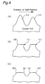
referring to, for example, Fig. 4 (a), apex portions of
the protrudent parts 112 are removed. Accordingly,
there inevitably occurs a directionality along which
mechanical polishing stress is applied. For example,
referring to Fig. 4, when apex portions of the
protrudent parts are polished by a rotary buff, stress
is applied to the apex portions of the protrudent parts
112 in the same direction as the direction of buff
rotation with the result that, as shown in Fig. 4 (b),
protrudent part portion first brought into contact with
the rotary buff is polished more easily than the side
later brought into contact with the rotary buff.
Furthermore, apex portions of the protrudent parts 112
are ground while being slightly deformed along the
direction of stress application, so that polished upper
portions of the protrudent parts may suffer from
deformation corresponding to the stress exerted by the
rotary buff or the like. For example, referring to Fig.
4 (b), it has been found that the protrudent parts may
be deformed along the direction of buff rotation with
the result that shelf-shape deformations 111 are formed
downstream in the direction of stress application.
As apparent from the above, stress is produced
during the mechanical polishing, so that the mechanical
polishing is inevitably accompanied by a directionality.
Further, in the process of the present invention, it is
intended to mainly polish and remove apex portions of
the protrudent parts of the matte side by the
mechanical polishing, but not to polish the whole
surface of the matte side so as to render the surface
specular. Rather, from the viewpoint of attaining
stable bonding to the surface of an insulating
substrate, it is preferred that the matte side surface
be not completely smooth. Therefore, in the present
invention, apex portions of the protrudent parts are
mainly mechanically polished. However, referring to
Fig. 4 (b), this mechanical polishing forms boundary
120 between polished portion and portion not polished.
When the matte side is directly subjected to the
subsequent treatment for roughening, the states of
being roughened may be different between the polished
portion and the portion not polished.
Therefore, in the present invention, referring to
Fig. 4 (c), the matte side having undergone the above
mechanical polishing is further chemically polished to
thereby remove discontinuous polishing boundary 120 and
instead create round curved surface 121. Moreover,
performing the chemical polishing after the mechanical
polishing can also correct the directionality of
polished surface due to stress, generated during the
mechanical polishing.
BRIEF DESCRIPTION OF THE DRAWING
Fig. 1 is a schematic sectional view of one form
of matte side of a conventional electrodeposited copper
foil;
Fig. 2 is a schematic sectional view showing the
state of the matte side having undergone buffing;
Fig. 3 is a schematic sectional view showing the
state of the matte side having undergone buffing and
subsequent chemical polishing;
Figs. 4 (A)-(C) schematically show the deformation
of protrudent parts made at buffing and after chemical
polishing;
Fig. 5 is a view schematically showing the state
of the electrodeposited copper foil with its surface
prepared that has been treated for roughening;
Fig. 6 is a view schematically showing the
electrodeposited copper foil with its surface prepared
of the present invention, having been laminated to a
polyimide film;
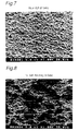
Fig. 7 is a Scanning Electron Micrometer (SEM)
photo showing one form of the matte side of an
electrodeposited copper foil before being subjected to
the process of the present invention;
Fig. 8 is a SEM photo showing one form of the
matte side having undergone the first mechanical
polishing;
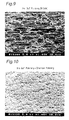
Fig. 9 is a SEM photo showing one form of the
matte side having undergone the second mechanical
polishing;
Fig. 10 is a SEM photo showing one form of the
matte side having undergone the chemical polishing; and
Fig. 11 is a SEM photo showing one form of the
matte side of an electrodeposited copper foil with its
surface prepared according to the present invention,
which has been treated for roughening.
DETAILED DESCRIPTION OF THE INVENTION
The electrodeposited copper foil with its surface
prepared according to the present invention, along with
the process for producing the same, will be described
in detail below with reference to the drawings. In the
drawings, like reference numerals are used to designate
like or corresponding members, if possible, throughout
the several views.
The electrodeposited copper foil prior to
mechanical polishing for use in the present invention
generally has a nominal thickness of 5 to 35 µm and an
average surface roughness (Rz) of matte side ranging
from about 2.5 to 10 µm, preferably about 3 to 8 µm.
Even with respect to electrodeposited copper foils of
small surface roughness, the average surface roughness
(Rz) of matte side is in the range of about 3 to 7 µm.
Examples of copper foils having such an average surface
roughness (Rz) include VLP foil (average surface
roughness (Rz): 3 to 5 µm) and HTE foil (average
surface roughness (Rz): 4 to 7 µm).
Fig. 1 is a sectional view schematically showing
the common surface condition of the matte side of an
electrodeposited copper foil (18 µm thick
electrodeposited copper foil) having an average gauge
thickness (T0) of 18 µm and an average surface
roughness (Rz0) of 3.6 µm. Fig. 2 is a schematic
sectional view of the electrodeposited copper foil
having its surface prepared so as to have an average
surface roughness (Rz1) of 2.0 µm by a mechanical
polishing. Fig. 3 is a schematic sectional view of the
electrodeposited copper foil having its surface
prepared so as to have an average surface roughness
(Rz2) of 1.5 µm with round shape by a chemical
polishing . Fig. 7 is a SEM photo showing the state of
matte side of the 18 µm thick electrodeposited copper
foil prior to polishing.
In Figs. 1 through 3, the designation "M side"
means the matte side of the electrodeposited copper
foil, and the designation "S side" means the shiny side
of the electrodeposited copper foil. Referring to Fig.
1, generally, the average surface roughness (Rz) of the
matte side is expressed by a 10-point average surface
roughness (Rz). The 10-point average roughness (Rz) is,
as shown in ISO 4287, an average of 10-points of five
largest values and five smallest values selected from
the specified lengths from depressed part bottom to
protrudent part apex at a multiplicity of points of the
matte side. The unevenness formed at the matte side is
not uniform, and the distance from the deepest bottom
of depressed parts to the highest apex of protrudent
parts (C0) is about 5 µm even in the electrodeposited
copper foil whose average surface roughness (Rz0) is
3.6 µm.
In the present invention, referring to Fig. 2, the
mechanical polishing mainly polishes apex portions of
the protrudent parts of the matte side. This
mechanical polishing causes the average surface
roughness (Rz1) of the matte side of the
electrodeposited copper foil to generally fall within
the range of 1.5 to 3.0 µm, preferably 1.8 to 2.5 µm.
This mechanical polishing can be accomplished by
the use of, for example, a rotary buff.
Specifically, while the electrodeposited copper
foil to be polished is being passed through guide rolls,
a rotary buff is pressed against the matte side thereof
to thereby effect intended polishing.
In this buffing, the buff is rotated in a single
direction at a rotating speed of generally 100 to 1500
rpm, preferably 1000 to 1300 rpm, to thereby effect
intended mechanical polishing. When the rotating speed
of the buff is less than 100 rpm, it is difficult to
uniformly polish the matte side to be polished. On the
other hand, when the rotating speed is much greater
than 1500 rpm, the buff rotation becomes unstable, so
that the electrodeposited copper foil may be broken.
Although the press force exerted by the buff upon
the electrodeposited copper foil to be polished in the
buffing can be appropriately regulated so as to avoid
breakage of the electrodeposited copper foil and
simultaneously avoid excess polishing of the matte side
by the buffing, it is generally preferred that the buff
press force in terms of buff motor current value be set
so as to fall within the range of 10.1 to 30 A (the
buff motor current value at the time of non-load is
about 10 A, so that the substantial press force of
buffing (substantial press force in terms of current)
in terms of buff motor current value is generally in
the range of about 0.1 to 20 A). Still preferably, the
substantial press force in terms of current is in the
range of 13 to 18 A. When the substantial press force
in terms of current is less than 0.1 A, either may
polishing of the electrodeposited copper foil be
ineffective, or the time required for polishing may be
extremely prolonged. On the other hand, when the
substantial press force in terms of current exceeds 20
A, breakage of the electrodeposited copper foil occurs
frequently.
When the electrodeposited copper foil is
mechanically polished by the above rotary buff, the
speed at which the copper foil to be polished is moved,
namely the line speed, is generally set so as to fall
within the range of 3 to 15 m/min. This line speed may
influence the uniformity of mechanical polishing. When
the line speed goes outside the above range, it is
likely for the uniformity of mechanical polishing to be
deteriorated.
In the above mechanical polishing, for example, in
the use of a buff, the type of employed polishing
material is not particularly limited. Use can be made
of, for example, a rotary buff of No. 800 to 3000 or so,
having aluminum oxide bonded thereto.
In the process of the present invention, although
one mechanical polishing is satisfactory, it is
preferred to carry out at least two mechanical
polishings. The reason is as follows. Since, in the
mechanical polishing, the matte side of the
electrodeposited copper foil is polished by, for
example, a rotary buff brought into contact with the
matte side, a relative mechanical polishing
directionality is generated by the direction of
rotation of the rotary buff and the direction of move
of the electrodeposited copper foil. Thus, one
mechanical polishing may induce, for example,
protrudent part deformation along the direction of
polishing (direction of buff rotation). The
directionality of mechanical polishing thus generated
on the matte side can be corrected to a certain extent
by, after the first buffing, polishing by means of the
second buff, which rotates in the direction reverse to
that of the first buff, brought into contact with the
matte side surface. Performing a plurality of
mechanical polishings in place of one mechanical
polishing enables reducing the polishing amount per
mechanical polishing. Thus, the press force of each
rotary buff can be set low, so that not only is the
possibility of breakage of polished electrodeposited
copper foil lowered but also the occurrence of
polishing directionality in each mechanical polishing
operation is suppressed.
When the mechanical polishing operation is thus
dispersed, it is preferred that each mechanical
polishing be performed under conditions set milder than
those mentioned above. When rotary buffs are employed,
it is preferred that the direction of rotation of the
second buff be reverse to that of the first buff.
Further, when use is made of a multiplicity of rotary
buffs including further the third buff, the fourth buff
and so on, it is preferred that the direction of
rotation of a rotary buff be reverse to that of the
preceding rotary buff. The buff grain size is
preferably equal to or smaller than that of the
preceding rotary buff.
The above polishing of the matte side of the
electrodeposited copper foil with the use of a
plurality of rotary buffs suppresses the occurrence of
streaks. These steaks are attributed to excess
grinding of the copper foil. The polishing in the
manner such that no steaks are generated not only
enables preventing the lowering of the mechanical
strength of the wiring pattern formed with the use of
this electrodeposited copper foil with its surface
prepared but also suppresses conduction failure and
other failures therein.
The above mechanical polishing selectively
polishes relatively high apex portions of the
protrudent parts of the matte side. For example,
polishing is performed so as to attain a reduction of
C0 = 5 µm for which reference is made to Fig. 1 to C1 =
2.5 to 3.2 µm for which reference is made to Fig. 2.
That is, this mechanical polishing causes C1 to attain
a reduction of 17 to 36% relative to the C0 prior to
surface preparing. When the level of the thus
performed mechanical polishing is evaluated by the
average surface roughness (Rz), the average surface
roughness (Rz) attained as a result of the mechanical
polishing is in the range of 1.5 to 3.0 µm, preferably
1.8 to 2.5 µm. For example, with respect to the
electrodeposited copper foil of Fig. 1, the original
average surface roughness (Rz0) is 3.8 µm, and the
mechanical polishing reduces the same to an average
surface roughness (Rz1) of 2.0 µm as shown in Fig. 2.
Thus, the mechanical polishing lowers the average
surface roughness (Rz) by 17 to 47%.
In the present invention, as aforementioned, it is
preferred that the mechanical polishing of the matte
side be performed at least twice. When the mechanical
polishing is performed at least twice, the polishings
are effected so that the total mechanical polishing
amount is as mentioned above.
Fig. 8 is a SEM photo showing the matte side of
the 18 µm thick electrodeposited copper foil having the
matte side as shown in Fig. 7, the matte side having
been buffed once. Fig. 9 is a SEM photo showing the
matte side, which matte side has thus undergone the
first buffing and thereafter the second buffing
performed with the use of the second rotary buff whose
direction of rotation is reversed from that of the
first buffing.
In the present invention, the matte side of the
electrodeposited copper foil is thus mechanically
polished at least once, and the mechanically polished
matte side is chemically polished.
As a chemical polishing solution for the
mechanically polished matte side, there can be employed,
for example, a nitric acid/sulfuric acid/hydrochloric
acid solution (bright dip solution), a solution
obtained by adding chromic acid to the bright dip
solution, a nitric acid type solution, a phosphoric
acid type solution, a chromic acid type solution, a
sulfuric acid type solution, a hydrogen peroxide type
solution, a sulfuric acid/hydrogen peroxide type
solution, a copper chloride type solution, an iron
chloride type solution, an ammonium persulfate type
solution and an ammonia/alkali type solution.
Specific examples of the polishing solutions which
can be employed in the present invention are indicated
below. The respective ingredient ratios of the
following polishing solutions are those typical with
respect to the concerned polishing solutions.
| nitric acid | 200 parts by volume |
| sulfuric acid | 400 parts by volume |
| hydrochloric acid | 2 parts by volume |
| water | 300 parts by volume. |
(2)
| nitric acid | 320 parts by volume |
| sulfuric acid | 640 parts by volume |
| hydrochloric acid |
| | 10 parts by volume |
| water | 640 parts by volume. |
(3)
| nitric acid | 20 to 80 parts by volume |
| sulfuric acid | 20 to 80 parts by volume |
| hydrochloric acid | 0.1 to 10 parts by volume |
| chromic acid | 5 to 200 parts by volume |
| water | appropriate amount. |
(4)
| phosphoric acid | 30 to 80 parts by volume |
| nitric acid | 5 to 20 parts by volume |
| glacial acetic acid | 10 to 50 parts by volume |
| water | appropriate amount. |
(5)
| phosphoric acid | 500 parts by volume |
| nitric acid | 200 parts by volume |
| glacial acetic acid | 50 parts by volume |
| hydrochloric acid | 5 parts by volume |
| water | 300 parts by volume. |
(6)
| phosphoric acid | 40 parts by volume |
| nitric acid | 15 parts by volume |
| hydrochloric acid | 1.5 parts by volume |
| water | 48 parts by volume |
| ammonium nitrate | 90 parts by weight. |
(7)
| phosphoric acid | 45 to 60 parts by volume |
| nitric acid | 8 to 15 parts by volume |
| sulfuric acid | 15 to 25 parts by volume |
| water |
| | 10 to 20 parts by volume. |
(8)
| chromic acid | 450 parts by weight |
| sulfuric acid | 125 parts by volume |
| hydrochloric acid | 5 parts by volume |
| glacial acetic acid | 75 parts by volume |
| water | 200 parts by volume. |
(9)
| sodium bichromate | 70 to 120 parts by weight |
| sulfuric acid | 100 to 200 parts by volume |
| benzotriazole | 2 to 40 parts by weight |
| water | q.s. ad 1000 parts by volume. |
(10)
| hydrogen peroxide | 100 mol/lit. |
| sulfuric acid | 2 mol/lit. |
| saturated alcohol | small amount. |
(11)
| hydrogen peroxide | 100 mol/lit. |
| hydrofluoric acid | 2 mol/lit. |
| saturated alcohol | small amount. |
(12)
| hydrogen peroxide | 100 mol/lit. |
| nitric acid | 2 mol/lit. |
| saturated alcohol | small amount. |
(13)
| nitric acid | 40 parts by volume |
| cuprous chloride | 3 parts by weight |
| glacial acetic acid | 60 parts by volume |
| potassium bichromate | 5 parts by weight |
| water | appropriate amount. |
(14)
| (NH4)3S2O2, etc. in terms of NH3 | 8.2 to 9.5 N |
| Cu | 150 to 180 g/lit. |
| pure water | remainder. |
Furthermore, examples of the commercially
available polishing solutions are as follows:
| DI (de ionized) pure water | 60.7 w/w% |
| sulfuric acid (62.5%) | 22.2 w/w% |
| hydrogen peroxide (35%) | 16.1 w/w% |
| Mec Power Etching HE 700 (trade name) | 1 w/w%. |
(16) (polishing solution produced by Meltex Inc.)
| Melpolish CU-67 (trade name) | 100 g/lit. |
| Melpolish CU-78B (trade name) | 50 ml/lit. |
| sulfuric acid (98%) | 75 ml/lit. |
| DI pure water | remainder. |
(17) (polishing solution produced by Shipley Inc.)
Chempolish 151 L-2 (trade name) solution as sold.
These chemical polishing solutions enable
polishing away a desired amount of copper from the
matte side by appropriately setting conditions for
bringing them into contact with the matte side of the
electrodeposited copper foil, for example, contact time
and agitation conditions.
For example, the surface of the matte side can be
converted into a desired polished form by immersing the
mechanically polished matte side in the chemical
polishing solution (bright dip solution) of item (1)
above at ordinary temperature for 10 to 30 sec. Also,
the surface of the matte side can be converted into a
desired polished form by immersing the mechanically
polished matte side in the chemical polishing solution
of item (3) above at 50 to 80°C for 2 to 6 min.
Generally, in the polishing solution containing nitric
acid/sulfuric acid/hydrochloric acid such as the bright
dip solution, the reaction is vehement, so that a given
level of chemical polishing can be accomplished by an
immersion conducted at room temperature or temperatures
close thereto for a relatively short period of time.
By contrast, when a phosphoric acid based solution is
employed, it is needed to contact the mechanically
polished matte side with the polishing solution warmed
(or heated) at ordinary temperature or higher for a
relatively prolonged period of time, for example, 1 to
a few minutes.
For example, referring to Fig. 3, the surface of
the mechanically polished matte side can be polished
nearly uniformly by contacting the mechanically
polished matte side with any of the above chemical
polishing solutions in the above manner. Further, for
example, shelf-shape portions formed during the
mechanical polishing, because of a large contact area,
are substantially completely removed. Still further,
these chemical polishing solutions are uniformly
brought into contact with the whole surface of the
matte side, and penetrate to portions which, for
example, the rotary buff failed to contact during the
mechanical polishing. Consequently, all the
mechanically polished matte side surface is chemically
polished in accordance with the area of contact with
the chemical polishing solution.
Therefore, the surface having been polished by the
chemical polishing operation shows a continuation of
gently-sloping curve as a whole, as shown in Fig. 3.
For example, when the chemical polishing is followed by
treatment for roughening, uniform treating of all the
matte side surface can be accomplished.
In the chemical polishing operation of the present
invention, it is intended to bring the chemical
polishing solution into selective contact with the
mechanically polished matte side, and it is not
intended to chemically polish the shiny side.
Therefore, generally, before contacting the
mechanically polished matte side with the chemical
polishing solution, the shiny side may be masked with
the use of, for example, an acidproof resin to thereby
protect the shiny side from the chemical polishing.
However, in the event that it is needed to chemically
polish the shiny side, the masking is not effected so
that the matte side and the shiny side can be
simultaneously chemically polished.
The above chemical polishing accomplishes
polishing of the whole matte side surface. For example,
polishing is performed so as to attain a reduction of
C1 = 3.2 µm for which reference is made to Fig. 2 to C2
= 2.6 µm for which reference is made to Fig. 3. That
is, the chemical polishing causes C2 for which
reference is made to Fig. 3 to attain a reduction of
20% relative to the C0 prior to surface polishing (Fig.
1). Thus, since the mechanical polishing as the prior
operation causes C1 to attain a reduction of 36%
relative to C0, the chemical polishing as the operation
subsequent to mechanical polishing causes C2 to attain
a reduction of 48% relative to C1. In the evaluation
of the level of thus performed chemical polishing by
the surface roughness changed by the chemical polishing,
the average surface roughness (Rz) becomes 0.8 to 2.5
µm, preferably 1.0 to 1.8 µm. For example, with
respect to the electrodeposited copper foil of Fig. 1,
the original average surface roughness (Rz0) is 3.6 µm,
and the mechanical polishing reduces the same to an
average surface roughness (Rz1) of 2.0 µm as shown in
Fig. 2. Thus, the mechanical polishing lowers the
average surface roughness (Rz) by 47%. The chemical
polishing reduces the same to an average surface
roughness (Rz2) of 1.5 µm as shown in Fig. 3. Thus,
the chemical polishing causes the average surface
roughness (Rz2) to attain a reduction of 60% relative
to the average surface roughness (Rz1) of matte side
accomplished by the mechanical polishing.
Moreover, shelf-shape portions formed during the
mechanical polishing are selectively chemically
polished by performing the chemical polishing after the
mechanical polishing. Therefore, the whole matte side
surface takes the form of a continuation of gently-sloping
curved shape. Consequently, in the treatment
for roughening generally conducted after the chemical
polishing, uniform treating of all the matte side
surface can be achieved.
Fig. 10 is a SEM photo showing the matte side of
the 18 µm thick electrodeposited copper foil having
undergone the two-stage buffing and thereafter the
above chemical polishing.
Assuming that the average thickness of the
electrodeposited copper foil before mechanical
polishing is 100%, the average thickness (gauge
thickness) of the 18 µm thick electrodeposited copper
foil whose matte side has thus been prepared by the
mechanical polishing followed by the chemical polishing
is in the range of 90 to 97%, preferably 94 to 96%,
based on the average thickness 100%. These values
suggest that the matte side of the electrodeposited
copper foil becomes a continuation of gently sloping
curved shape and that, taking into account the average
surface (Rz1) of the matte side before polishing, there
is no conspicuous change in the thickness of
electrodeposited copper foil overall. That is, most
apex portions of the protrudent parts of the matte side
are ground by the mechanical polishing followed by the
chemical polishing according to the present invention,
and streaks attributed to the mechanical polishing,
such as pointed streaks often observed on the
mechanically polished surface, are eliminated by the
chemical polishing. Therefore, in the process of the
present invention, any conspicuous decrease of strength
of electrodeposited copper foil attributed to polishing
would not result from the mechanical polishing followed
by the chemical polishing even when use is made of an
extremely thin electrodeposited copper foil (for
example, average thickness: 12 to 18 µm).
In the present invention, after the above
preparing of the matte side of electrodeposited copper
foil by the mechanical polishing followed by the
chemical polishing, it is preferred that the prepared
matte side be treated for roughening as shown in Fig. 5.
This treatment sticks fine particles of copper to
the thus prepared matte side. In this treatment, fine
particles of copper are formed on the prepared matte
side by the use of plating techniques conducted under
different conditions in combination.
For maintaining etching properties while enhancing
the adherence of the copper foil to an insulating
substrate, it is preferred that the mechanically
polished surface of the copper foil be treated so that
the average surface roughness (Rz) falls within the
range of 1.5 to 4.0 µm, especially 1.5 to 3.5 µm, and
still especially 1.5 to 2.5 µm. The matte side can be
uniformly polished by the mechanical polishing
operation followed by the chemical polishing operation,
and the resultant uniform polished surface accomplishes
uniform electrodeposition of fine copper particles at a
high density.
This treatment comprises a sequence of burn
plating, seal plating and whisker plating. This
sequence of plating operations are carried out under,
for example, the following conditions.
(1) Burn plating
An insoluble electrode is arranged opposite to the
matte side of an electrodeposited copper foil which has
been prepared by the mechanical polishing followed by
the chemical polishing, and a plating is carried out
under the following conditions:
A layer of particulate copper electrodeposits
known as "burn plating" is formed on the prepared matte
side of the electrodeposited copper foil by the
electroplating conducted under these conditions.
(2) Seal plating
Subsequently, the surface having undergone the
above burn plating is subjected to a seal plating
conducted under the following conditions:
The above layer of particulate copper
electrodeposits is coated with a thin film of copper
known as "seal plating" by the plating conducted under
these conditions.
(3) Whisker plating
Thereafter, the surface having undergone the above
seal plating is subjected to a whisker plating
conducted under the following conditions:
Whiskery copper deposits known as "whisker
plating" are formed on the copper covering film having
been formed by the above seal plating by the plating
conducted under these conditions.
Fig. 11 is a SEM photo showing the matte side of
18 µm thick electrodeposited copper foil having
undergone the above treatment.
The above describes only an example of roughening
treatment, and desired nodulation can be adopted under
other customarily employed roughening treatment
conditions.
After the above treatment for roughening, the
prepared matte side is preferably passivated. This
passivation is a plating of a metal which is
electrochemically baser than copper, such as zinc or
chromium, to the above treated surface. For example, a
thin plating layer of a metal having corrosion
preventive properties for copper is formed on the
treated surface.
In particular, for example, the passivation based
on zinc and/or chromate can be accomplished by a
sequence of operations consisting of treating an
electrodeposited copper foil with its matte side
surface prepared by the above mechanical polishing
followed by the chemical polishing, passing the treated
electrodeposited copper foil through a zinc plating
bath and performing chromate treatment.
Employable zinc treatment conditions are, for
example, as follows.
In the zinc treatment, the treated matte side is
electro-plated with zinc at a current density of 5
A/dm2 for 8 sec. through, for example, a 25°C plating
solution having a zinc concentration of 5 g/lit. and a
sulfate concentration of 50 g/lit.
After the formation of a zinc plating layer, the
surface of the zinc plating layer is subjected to a
chromate treatment.
This chromate treatment is performed by, for
example, electolyzing at a current density of 1 A/dm2
for 5 sec. through a pH 4 electrolytic solution having
a chromic anhydride concentration of 2 g/lit. Further,
the surface having undergone the above chromate
treatment is preferably coated with, for example, a
silane compound such as γ-glycidoxypropyltrimethoxysilane
as a silane coupling
agent to thereby form a silane coupling agent layer.
When, for example, the above 18 µm thick
electrodeposited copper foil is subjected to the above
mechanical polishing, chemical polishing, treatment for
roughening, passivation and chromate treatment, the
resultant electrodeposited copper foil generally has an
average thickness (gauge thickness) of 16 to 20 µm,
preferably 17 to 19 µm.
The electrodeposited copper foil of the present
invention (preferably, the electrodeposited copper foil
with its surface prepared and treated for roughening)
having undergone the passivation and chromate treatment
after the treatment for roughening generally has an
average thickness of 5 to 35 µm, preferably 12 to 25 µm.
Assuming that the average thickness of the
electrodeposited copper foil before surface preparing
is 100%, the average thickness of the thus prepared
electrodeposited copper foil with its surface prepared
(preferably, the electrodeposited copper foil with its
surface prepared and treated for roughening) is
generally in the range of 90 to 97%, preferably 94 to
96%. This means that there is no conspicuous polishing
loss of copper. Moreover, the average surface
roughness (Rz) of the matte side of the above obtained
18 µm thick electrodeposited copper foil with its
surface prepared and treated (electrodeposited copper
foil with its surface prepared, obtained by performing
the treatment for roughening after the polishings) is
generally in the range of 1.0 to 3.0 µm, preferably 2.0
to 2.5 µm. For example, at the bonding to an
insulating film through an adhesive layer, a very
uniform and high bond strength can be attained
therebetween.
The mechanical polishing followed by the chemical
polishing not only selectively polishes protrudent
parts of the matte side but also realizes the form of a
continuation of gently sloping curved shape on the
overall matte side surface. Extremely uniform
roughening treatment (nodulation) can be obtained on
this polished surface.
In the process of the present invention, the matte
side of the electrodeposited copper foil is selectively
mechanically polished and subsequently chemically
polished. During the chemical polishing, it is common
practice to mask the shiny side (average surface
roughness generally ranges from about 1.2 to 2.5 µm) to
prevent the surface roughness is varied by the
polishing.
A printed wiring board can be produced by
laminating a substrate with the thus produced
electrodeposited copper foil with its surface prepared,
preferably electrodeposited copper foil with its
surface prepared and treated for roughening,
subsequently applying a photoresist layer to thereby
effect masking and thereafter leaching excess copper to
thereby form a wiring pattern on the substrate.
That is, in the printed wiring board of the
present invention, a wiring pattern formed from the
electrodeposited copper foil with its surface prepared,
preferably the electrodeposited copper foil with its
surface prepared and treated for roughening, is
disposed on the surface of an insulating substrate.
This electrodeposited copper foil with its surface
prepared is the described one having a shiny side and a
prepared matte side whose average surface roughness
(Rz) is in the range of 0.8 to 2.5 µm, the above
prepared matte side obtained through the steps of
subjecting a matte side of electrodeposited copper foil
whose average surface roughness (Rz) is in the range of
2.5 to 10 µm to at least one mechanical polishing so
that the average surface roughness (Rz) of the matte
side becomes in the range of 1.5 to 3.0 µm, and
subjecting the matte side having undergone the
mechanical polishing to a selective chemical polishing
so that the average surface roughness (Rz) of the matte
side becomes in the range of 0.8 to 2.5 µm.
Referring to Fig. 6, the printed wiring board of
the present invention comprises insulating substrate 10
and, superimposed on at least one side thereof, wiring
pattern 14. This wiring pattern can be formed by first
laminating the insulating substrate with the
electrodeposited copper foil with its surface prepared,
preferably electrodeposited copper foil with its
surface prepared and treated, through an adhesive or
without the use of any adhesive, and thereafter etching
the copper foil to perform desired pattern. The
laminating of the insulating substrate with the
electrodeposited copper foil with its surface prepared,
preferably electrodeposited copper foil with its
surface prepared and treated, is conducted in such a
manner that the prepared matte side faces the
insulating substrate.
The insulating substrate 10 can be laminated with
the electrodeposited copper foil with its surface
prepared (preferably electrodeposited copper foil with
its surface prepared and treated) by compressing them
to each other while heating with or without a
thermosetting adhesive 12 interposed therebetween.
Various substrates such as a glass reinforced
synthetic resin substrate and a paper reinforced
synthetic resin substrate can be employed as the
insulating substrate 10 for use in the present
invention. It is preferred that the employed
insulating substrate have a chemical resistance
ensuring freedom from deterioration by chemical
solutions from the viewpoint that the insulating
substrate is brought into contact with an acid, etc. at
the time of etching. Further, it is preferred that the
insulating substrate have a heat resistance ensuring
freedom from deterioration by heating made at the time
of bonding of devices, etc. The insulating substrate
can be produced from various resins, examples of which
include a glass reinforced epoxy, a BT (Bismaleimide
Triazine), polyesters, polyamides, fluororesins (e.g.,
Teflon (trade name)), liquid crystal polymers and
polyimides. Especially in the present invention, when
a flexible insulating substrate is employed as the
insulating substrate, it is preferred to use a film
insulating substrate composed of a polyimide.
The polyimide substrate for constituting the
insulating substrate 10 can be produced from, for
example, a totally aromatic polyimide synthesized from
pyromellitic acid dianhydride and an aromatic diamine
or a totally aromatic polyimide of biphenyl skeleton
synthesized from biphenyltetracarboxylic acid
dianhydride and an aromatic diamine. Especially in the
present invention, a totally aromatic polyimide of
biphenyl skeleton (e.g., Upilex (trade name) produced
by Ube Industries, Ltd.) is preferably used as the
polyimide film. When the insulating substrate in film
form is used in the present invention, the thickness of
the insulating substrate 10 is generally in the range
of 25 to 125 µm, preferably 50 to 75 µm.
The insulating substrate 10, depending on the use
thereof, may be furnished with through-holes such as
device holes, sprocket holes and outer lead cut holes.
These through-holes are generally formed by die
punching.
The wiring pattern 14 can be formed by first
laminating the above insulating substrate 10 furnished
with needed holes with the electrodeposited copper foil
with its surface prepared (preferably electrodeposited
copper foil with its surface prepared and treated)
through an insulating adhesive 12 so that the prepared
matte side of the electrodeposited copper foil contacts
the adhesive layer 12, subsequently applying a resist,
and thereafter etching the electrodeposited copper foil
with its surface prepared (preferably electrodeposited
copper foil with its surface prepared and treated).
The lamination of the insulating substrate with
the electrodeposited copper foil with its surface
prepared (preferably electrodeposited copper foil with
its surface prepared and treated) can be performed with
the use of an adhesive or without any adhesive layer
interposed therebetween. In the use of an adhesive,
the employed adhesive 12 must have properties such as
heat resistance, chemical resistance, bond strength and
flexibility. For example, epoxy adhesives and phenol
adhesives can be mentioned as the adhesive having these
properties. These adhesives may be those modified with
a urethane resin, a melamine resin, a polyvinylacetal
resin and the like, and the epoxy resin per se may be
one modified with a rubber. These adhesives are
thermosetting. These adhesives are applied in the form
of a layer whose thickness is generally in the range of
3.7 to 23 µm, preferably 10 to 21 µm. When use is made
of the adhesives, the adhesive layer may be applied to
the surface of the insulating substrate 10, or to the
matte side of the electrodeposited copper foil with its
surface prepared.
Photoresist is applied to the shiny side of the
electrodeposited copper foil with its surface prepared
(preferably electrodeposited copper foil with its
surface prepared and treated) thus superimposed on the
insulating substrate 10 by lamination. Wiring pattern
is printed, and development is conducted to thereby
remove excess photoresist, followed by etching. Thus,
the wiring pattern 14 is obtained.
After the formation of the wiring pattern on the
surface of the insulating substrate 10 in the above
manner, a protective resin such as a solder resist can
be applied to parts other than bonding or connecting
parts (lead parts) for device bonding. After the
application of the protective resin, the lead parts for
device bonding are subjected to nickel/gold plating,
tin plating, solder plating or gold plating. Although
in most cases the protective resin is first applied and
subsequently the parts not furnished with the
protective resin are plated as mentioned above, it is
feasible to first form a thin plating layer of the
above metal on the surface of wiring pattern formed
prior to the application of protective resin, next
apply a protective resin and thereafter plate lead
parts extending out of the protective resin, for
example, in order to prevent any whisker generation and
to avoid any abnormal corrosion of wiring pattern by
the plating solution. This plating method is useful
especially when the tin plating which is likely to
invite whisker generation is employed.
After the above formation of the plating layer,
device mounting can be carried out by the use of any of
common methods, such as the wire bonding method, TAB
(Tape Automated Bonding) method, flip chip bonding
method. After the device mounting, generally, the
device carrying PWB (printed wiring board) is sealed
with the application of a seal resin to the devices and
connected to PWB by soldering, BGA (Ball Grid Array)
method, Anisotropic Conductive Film method, etc.
altogether and put to practical use.
In the present invention, a multilayer laminate
can be provided by laminating the above PWBs and by
securing electrical connection in the direction of the
laminate thickness.
That is, the multilayer printed wiring board of
the present invention comprises a laminate of a
plurality of boards of given thickness, each of the
boards having its surface furnished with a wiring
pattern, the above boards capable of being electrically
connected to each other in the direction of the
thickness of the laminate. The copper foil for forming
the wiring pattern in the multilayer printed wiring
board of the present invention is an electrodeposited
copper foil with its surface prepared having a shiny
side and a prepared matte side whose average surface
roughness (Rz) is in the range of 0.8 to 2.5 µm, the
prepared matte side obtained through the steps of
subjecting a matte side of electrodeposited copper foil
whose average surface roughness (Rz) is in the range of
2.5 to 10 µm to at least one mechanical polishing so
that the average surface roughness (Rz) of the matte
side becomes in the range of 1.5 to 3.0 µm, and
subjecting the matte side having undergone the
mechanical polishing to a chemical polishing so that
the average surface roughness (Rz) of the matte side
becomes in the range of 0.8 to 2.5 µm. In the present
invention, it is especially preferred to employ an
electrodeposited copper foil with its surface prepared
and treated for roughening.
The electrical connection in the direction of the
laminate thickness can be secured by various methods,
for example, the method comprising making via holes in
PWBs by, for example, a drill or laser and either
depositing a conductive metal on the wall of the via
holes or filling a conductive resin composition
containing a conductive metal into the via holes, or
the method comprising forming conductive bumps on PWBs
with the utilization of printing technique and mutually
connecting the conductive bumps.
The electrodeposited copper foil with its surface
prepared according to the present invention is suitable
for use in PWBs, such as TAB tapes, flexible printed
wiring boards, multilayer printed wiring boards and
rigid flex. In view of strikingly uniform preparing of
the matte side together with uniform treatment thereof
for roughening, the electrodeposited copper foil with
its surface prepared according to the present invention
is especially suitable for use as an extremely thin
electrodeposited copper foil whose consumption is
expected to increase in accordance with the recent
trend toward fine pitch.
EFFECT OF THE INVENTION
The electrodeposited copper foil with its surface
prepared according to the present invention is obtained
by sequentially subjecting the matte side to the
mechanical polishing and the chemical polishing. The
mechanical polishing mainly polishes apex portions of
the protrudent parts of the matte side, and the
subsequent chemical polishing further uniformly
eliminates shelf-shape deformation on the mechanically
polished matte side. In the electrodeposited copper
foil with its surface prepared according to the present
invention, obtained by sequentially subjecting the
matte side to the mechanical polishing and the chemical
polishing, mechanical polishing traces formed along the
mechanical polishing direction and strain layers,
generated by the mechanical polishing operation, are
eliminated by the chemical polishing to thereby enable
forming a strikingly uniform matte side surface.
Treating for roughening the thus prepared matte side of
the electrodeposited copper foil with its surface
prepared enables uniformly forming fine particles of
copper on the matte side (electrodeposited copper foil
with its surface prepared and treated). The PWB
obtained by laminating, for example, an insulating
substrate with the thus obtained electrodeposited
copper foil with its surface prepared according to the
present invention and forming the copper foil into a
wiring pattern exhibits a high peel strength between
the wiring pattern and the insulating substrate and
further ensures an overall stable strength. Moreover,
in the process of the present invention, not only are
apex portions of the protrudent parts of the matte side
mainly mechanically polished but also the polishing
irregularity, streaks, strain, etc., resulting from the
mechanical polishing, are eliminated by the chemical
polishing. Thus, the copper loss by polishing is
strikingly slight, and the matte side surface
consisting of a continuous curved shape can be obtained.
This roughening treatment of the matte side
enables performing uniform nodulating treatment of the
prepared matte side. Thus, PWB capable of exhibiting
high performance in adhesive strength, bonding
reliability, etc. can be obtained.
In the process of the present invention, the matte
side of the electrodeposited copper foil is
sequentially subjected to the mechanical polishing
performed under mild conditions and the chemical
polishing, so that the occurrence of streaks and the
like on the polished matte side can be suppressed. The
streaks are generally attributed to excess polishing,
and the electrodeposited copper foil of this part is
thinner there than at other parts. Thus, when the
electrodeposited copper foil having streaks is employed
in the use of an extremely thin copper foil in
accordance with the trend toward fine pitch, the
mechanical strength of wiring pattern there is reduced
with the result that the streak portions are likely to
become the cause of failure such as open circuit. The
electrodeposited copper foil with its surface prepared,
produced by the process of the present invention, is
free from such streaks attributed to excess polishing,
so that, with respect to wiring boards such as PWB
produced with the use of the prepared electrodeposited
copper foil, the occurrence of defective items
attributed to such an open circuit or the like is
strikingly low.
Moreover, when the electrodeposited copper foil
with its surface prepared according to the present
invention is formed into a wiring pattern through
superimposing the same on an insulating substrate by
laminating or bonding after resist application and
etching, the difference between upper edge width and
lower edge width of the formed wiring (especially lead
parts) is minute. Thus, a wiring of approximately
rectangular cross section can be formed. In the use of
the conventional electrodeposited copper foil, the
lower edge tends to be larger and wavier than the upper
edge in the formed wiring, thereby causing the cross
section configuration to be trapezoidal. However, in
the use of the electrodeposited copper foil with its
surface prepared according to the present invention,
the above trend is eliminated, and a wiring of
approximately rectangular cross section can be obtained.
Furthermore, the lower edge portions of the wiring are
etched linearly, and there is substantially no copper
residue on the insulating substrate. These
characteristics, although important in, for example,
inner leads as well, are especially important in output
side outer leads electrically connected to liquid
crystal elements, and the like. With respect to the
output side outer leads electrically connected to
liquid crystal elements, a plurality thereof are
connected to liquid crystal pixels, and not only is the
lead width thereof extremely small but also the pitch
is rendered small. Accordingly, the output side outer
leads are likely to suffer from insulation failure
between neighboring leads. For example, even if the
linearity of output side outer leads is slightly
deteriorated, there is the danger of insulation failure
(short circuit). Further, if the lower edge is
slightly wider than the upper edge in the output side
outer leads, there is the danger of insulation failure
(short circuit) on the surface of the insulating
substrate. Still further, even if slight copper
residue exists on the insulating substrate, there is
the danger of insulation failure (short circuit). In
the output side outer lead parts of PWBs (especially
TAB tape) connected to liquid crystal elements, etching
of the copper foil must be achieved with precision
equal to or higher than that for inner leads for
mounting electronic components. Especially, with
respect to the output side outer leads of the TAB tape
for liquid crystal elements, these must be formed on an
insulating substrate by etching the electrodeposited
copper foil disposed on the insulating substrate by
laminating, so that each of the leads is likely to have
a trapezoidal cross section as compared with inner
leads which extend out into device holes and under
which any insulating substrate is not present. Further,
due to the presence of the insulating substrate, copper
residue is likely to occur. Therefore, it is believed
that the achievement of fine pitch is more difficult in
the output side outer leads than in the inner leads.
However, the above achievement of fine pitch in
the output side outer leads can be enabled by the use
of the electrodeposited copper foil with its surface
prepared according to the present invention.
Specifically, by virtue of the use of the
electrodeposited copper foil with its surface prepared
according to the present invention, not only do the
output side outer leads formed by etching have a
rectangular cross section (upper edge width being
substantially the same as the lower edge width) but
also the linearity of formed leads is high. Further,
there is no copper residue on the surface of the
insulating substrate. Although the particular reason
for the above excellent etching properties of the
electrodeposited copper foil with its surface prepared
according to the present invention has not yet been
elucidated, specific exertion of the above effects of
the present invention would be achieved by the
mechanical polishing followed by the chemical polishing.
In the electrodeposited copper foil with its
surface prepared according to the present invention, as
aforementioned, the matte side is highly uniformly
prepared, and uniform roughening can be accomplished by
treating the uniform matte side. By virtue of this
uniform roughening, not only desirable bonding to an
insulating substrate be attained but also device
mounting on PWB can be secured by plating the thus
uniformly treated surface.
As apparent from the above, the electrodeposited
copper foil with its surface prepared, obtained by the
process of the present invention, ensures not only high
adherence to insulating substrates but also strikingly
high yield of device mounting on boards.
Furthermore, the use of the electrodeposited
copper foil with its surface prepared according to the
present invention enables obtaining PWB and multilayer
laminate PWB of stable properties.
The PWB and multilayer laminate PWB produced with
the use of the electrodeposited copper foil whose matte
side has been prepared according to the present
invention exhibit strikingly high bondability (bonding
reliability) for mounted devices.
EXAMPLE
The present invention will now be illustrated in
greater detail with reference to the following Example,
which in no way limits the scope of the invention.
EXAMPLE 1
An electrodeposited copper foil (VLP foil) of 18
µm gauge thickness having an average surface roughness
of shiny side of 1.2 µm and an average surface
roughness (Rz1) of matte side of 3.6 µm was provided.
A SEM photo of the matte side of the VLP foil is shown
in Fig. 7.
While the VLP foil was being passed through guide
rolls, the matte side of the VLP foil was buffed by
means of # 1000 buff comprising aluminum oxide as
abrasive grains (manufactured by Tsunoda Brush K.K.),
arranged so that the direction of buff rotation was
counter to the direction of advance of electrodeposited
copper foil, under conditions such that the first-stage
buff rotating speed, press force in terms of buff motor
current value and line speed were 1200 rpm, 19 A and 8
m/min, respectively the first mechanical polishing).
A SEM photo of the matte side having undergone the
first mechanical polishing is shown in Fig. 8.
After the first mechanical polishing of the VLP
foil, the matte side having undergone the first
mechanical polishing was buffed by means of # 1000 buff
while being rotated in the direction identical with the
direction of advance of VLP foil. At this buffing, the
second-stage buff rotating speed, press force in terms
of buff motor current value and line speed were 1200
rpm, 1.6 A and 8 m/min, respectively (the second
mechanical polishing).
The rotation current value at the time of non-load
was 10 A when measured in the first buffing and 18 A
when measured in the second buffing.
A SEM photo of the matte side of the VLP foil thus
having undergone the two mechanical polishings is shown
in Fig. 9. The average surface roughness (Rz) of the
thus mechanically polished matte side was 2.0 µm, which
indicated a mechanical polishing of 18% relative to the
average surface roughness (Rz) of the matte side of the
VLP foil prior to the mechanical polishings. As seen
from Fig. 8, streaks remained on the matte side,
irrespective of the performing of the twice mechanical
polishings.
After the mechanical polishings, the shiny side
was coated with an acidproof resin to thereby effect
masking thereof.
The VLP foil whose shiny side was masked was
immersed in the chemical polishing solution of the
following composition and chemically polished at 30°C
for 5 sec. while the chemical polishing solution was
being circulated.
Fundamental composition of chemical polishing
solution
| Ingredient | Content |
| (1) | CuCl2 | 80 parts by weight |
| (2) | 35% HCl | 50 parts by weight |
| (3) | 30% H2O2 | 20 parts by weight |
| (4) | water | (q.s. ad 1000 parts by volume). |
This chemical polishing solution was constantly in
contact with the matte side by means of a circulatory
chemical polishing apparatus. This circulatory
chemical polishing apparatus was equipped with a built-in
automatic analyzer of the composition of the
chemical polishing solution. The circulatory chemical
polishing apparatus was also equipped with an
ingredient supplying means for restoring the
composition to the fundamental composition when the
composition of the chemical polishing solution had a
variation of 5 to 15% relative to the fundamental
composition.
After the above chemical polishing of the matte
side, the VLP foil with its surface prepared was well
washed with water. A SEM photo of the prepared matte
side after the chemical polishing is shown in Fig. 10.
As a result of this chemical polishing, there was
obtained a prepared matte side which was nearly
completely free of streaks observed on mechanically
polished matte sides, such as polishing directionality
and shelf-shape pointed portions resulting from
mechanical polishing, and which as a whole assumed the
form of a continuation of curved shape. The average
surface roughness (Rz) of the thus chemically polished
matte side was 1.5 µm, which suggested that the
chemical polishing operation achieved a polishing of
25% relative to the average surface roughness (Rz) of
the matte side of the VLP foil having undergone the
mechanical polishing.
The average gauge thickness of the VLP foil with
its surface prepared, obtained by the mechanical
polishing followed by the chemical polishing, was about
16.8 µm, while that of the VLP foil prior to mechanical
polishing employed in this Example was 17.1 µm. These
suggested that there was no conspicuous copper loss
attributed to leaching of copper from the VLP foil.
The matte side of the VLP copper foil with its
matte side surface thus prepared was treated for
roughening. This treatment effected nodulation of the
prepared matte side by the use, in combination, of a
plurality of plating operations consisting of burn
plating, seal plating and whisker plating. In this
Example, the treatment was carried out by the use of
plating solutions of the following compositions.
(1) Burn plating
An insoluble electrode was arranged opposite to
the buffed matte side of the electrodeposited copper
foil, having been prepared by the mechanical polishing
followed by the chemical polishing, and electroplating
was carried out under the following conditions:
A layer of particulate copper electrodeposits was
formed on the surface of the electrodeposited copper
foil with its surface prepared by the burn plating
conducted under these conditions.
(2) Seal plating
After the above burn plating, a covering plating
was performed under the following conditions:
A thin film of copper known as "seal plating" was
formed by this seal plating so as to cover the copper
electrodeposits having been formed by the burn plating.
(3) Whisker plating
Thereafter, the surface having undergone the above
covering plating was subjected to a whisker plating
conducted under the following conditions:
Whiskery copper deposits known as "whisker
plating" were formed on the copper coating film having
been formed by the above seal plating by the
electroplating conducted under these conditions.
The matte side of the VLP foil having thus been
polished and treated for roughening was observed
through a SEM photo. A SEM photo of the matte side is
shown in Fig. 11.
The average surface roughness (Rz) of the thus
treated matte side was 2.5 µm. The average thickness
(gauge thickness) of the electrodeposited copper foil
with its surface prepared and treated in the above
manner was 17.5 µm. Thus, this treatment attained a
recovery to about 98% based on the average thickness of
the electrodeposited copper foil. As apparent from a
comparison of Fig. 7 showing the direct treatment of
the matte side of the VLP foil used as a raw material
to Fig. 11 showing the treatment conducted after the
preparing in the above manner, strikingly uniform
treatment of the matte side can be accomplished with
respect to the electrodeposited copper foil with its
surface prepared, obtained by the process of the
present invention, for example, by the above performing
of mechanical polishing, chemical polishing and
treatment for roughening in sequence.
The treated side of the thus obtained
electrodeposited copper foil with its surface prepared
and treated for roughening was furnished with a
corrosion preventive layer. This corrosion preventive
layer was formed with the use of zinc. This zinc
passivation was performed at a current density of 5
A/dm2 for 8 sec in a 25°C plating solution having a
zinc concentration of 5 g/lit. and a sulfate
concentration of 50 g/lit. The formed zinc layer was
extremely thin, and the thickness thereof was generally
100 Å or less.
After the above formation of the zinc layer, an
electrolytic chromating thereof was performed at a
current density of 1 A/dm2 for 5 sec in a pH 4
electrolytic solution having a chromic anhydride
(chromium trioxide) concentration of 2 g/lit. After
the chromate treatment, the surface of a chromate layer
was coated with γ-glycidoxypropyltrimethoxysilane.
The thus obtained VLP foil with its surface
prepared and treated (after the plating of the
passivation layer, chromate layer and silane coupling
agent layer) was arranged so that the prepared matte
side faced one side of a 125 µm thick polyimide
substrate (with a thermosetting adhesive) furnished
with sprocket holes and device holes, and bonded by hot
press to each other. Subsequently, a photoresist was
applied to the surface of the electrodeposited copper
foil with its surface prepared and treated, and exposed
to radiation in desired wiring pattern. Excess
photoresist was removed, and non-masked copper foil was
removed by etching. Thus, a wiring pattern was formed.
The photoresist was removed, and the wiring
pattern at parts other than lead ends for bonding was
coated with a solder resist. Further, a tin plating
layer was formed, thereby obtaining PWB.
The thus obtained PWB exhibited a strikingly low
failure ratio with respect to the open circuit of the
wiring pattern. Further, the wiring pattern and the
polyimide substrate were bonded to each other with high
stability. Still further, the tensile strength of the
lead was high. A section of formed lead was observed,
and was found to be rectangular. No copper residue was
detected on the substrate.
Two PWBs produced in the above manner were bonded
to each other with the use of an insulating resin.
Subsequently, using laser, through holes were formed so
that they passed through both the upper layer wiring
pattern and the lower layer wiring pattern. Conductive
metal was deposited on the wall of the formed through
holes by the electroless plating technique to thereby
enable electrical connection between the upper layer
and the lower layer. The resultant multilayer laminate
PWB was sealed with a resin.
The thus obtained multilayer laminate PWB
exhibited a low failure ratio and possessed strikingly
stable properties.