EP1082744B1 - Display with encapsulated matrix structure - Google Patents
Display with encapsulated matrix structure Download PDFInfo
- Publication number
- EP1082744B1 EP1082744B1 EP99925701A EP99925701A EP1082744B1 EP 1082744 B1 EP1082744 B1 EP 1082744B1 EP 99925701 A EP99925701 A EP 99925701A EP 99925701 A EP99925701 A EP 99925701A EP 1082744 B1 EP1082744 B1 EP 1082744B1
- Authority
- EP
- European Patent Office
- Prior art keywords
- prevention structure
- display device
- field emission
- porous material
- contaminant prevention
- Prior art date
- Legal status (The legal status is an assumption and is not a legal conclusion. Google has not performed a legal analysis and makes no representation as to the accuracy of the status listed.)
- Expired - Lifetime
Links
- 239000011159 matrix material Substances 0.000 title claims description 160
- 239000000356 contaminant Substances 0.000 claims description 167
- 230000002265 prevention Effects 0.000 claims description 112
- 238000000576 coating method Methods 0.000 claims description 62
- 239000011148 porous material Substances 0.000 claims description 61
- 239000011248 coating agent Substances 0.000 claims description 57
- 239000000463 material Substances 0.000 claims description 56
- VYPSYNLAJGMNEJ-UHFFFAOYSA-N Silicium dioxide Chemical compound O=[Si]=O VYPSYNLAJGMNEJ-UHFFFAOYSA-N 0.000 claims description 41
- 239000004642 Polyimide Substances 0.000 claims description 34
- 229920001721 polyimide Polymers 0.000 claims description 34
- 229910052814 silicon oxide Inorganic materials 0.000 claims description 18
- 229910052782 aluminium Inorganic materials 0.000 claims description 16
- XAGFODPZIPBFFR-UHFFFAOYSA-N aluminium Chemical compound [Al] XAGFODPZIPBFFR-UHFFFAOYSA-N 0.000 claims description 16
- 238000003795 desorption Methods 0.000 claims description 14
- 239000000126 substance Substances 0.000 claims description 7
- 230000008018 melting Effects 0.000 claims description 6
- 238000002844 melting Methods 0.000 claims description 6
- 239000007787 solid Substances 0.000 claims description 6
- 239000008119 colloidal silica Substances 0.000 claims description 5
- 229910003480 inorganic solid Inorganic materials 0.000 claims description 4
- 229910052751 metal Inorganic materials 0.000 claims description 4
- 239000002184 metal Substances 0.000 claims description 4
- 229910052790 beryllium Inorganic materials 0.000 claims description 3
- ATBAMAFKBVZNFJ-UHFFFAOYSA-N beryllium atom Chemical compound [Be] ATBAMAFKBVZNFJ-UHFFFAOYSA-N 0.000 claims description 3
- 238000010943 off-gassing Methods 0.000 claims description 3
- 239000010410 layer Substances 0.000 description 87
- OKTJSMMVPCPJKN-UHFFFAOYSA-N Carbon Chemical compound [C] OKTJSMMVPCPJKN-UHFFFAOYSA-N 0.000 description 12
- 239000004020 conductor Substances 0.000 description 11
- 229910002804 graphite Inorganic materials 0.000 description 11
- 239000010439 graphite Substances 0.000 description 11
- 238000000151 deposition Methods 0.000 description 10
- 238000001704 evaporation Methods 0.000 description 10
- 230000008020 evaporation Effects 0.000 description 10
- 238000004544 sputter deposition Methods 0.000 description 10
- 239000000377 silicon dioxide Substances 0.000 description 9
- 235000012239 silicon dioxide Nutrition 0.000 description 9
- 238000005229 chemical vapour deposition Methods 0.000 description 8
- 230000002939 deleterious effect Effects 0.000 description 8
- 239000000470 constituent Substances 0.000 description 7
- 230000015572 biosynthetic process Effects 0.000 description 6
- 238000011109 contamination Methods 0.000 description 6
- 230000035515 penetration Effects 0.000 description 6
- 239000000084 colloidal system Substances 0.000 description 5
- 239000007921 spray Substances 0.000 description 5
- XUIMIQQOPSSXEZ-UHFFFAOYSA-N Silicon Chemical compound [Si] XUIMIQQOPSSXEZ-UHFFFAOYSA-N 0.000 description 4
- 230000007423 decrease Effects 0.000 description 4
- AMGQUBHHOARCQH-UHFFFAOYSA-N indium;oxotin Chemical compound [In].[Sn]=O AMGQUBHHOARCQH-UHFFFAOYSA-N 0.000 description 4
- 229910052710 silicon Inorganic materials 0.000 description 4
- 239000010703 silicon Substances 0.000 description 4
- 230000002411 adverse Effects 0.000 description 3
- 230000008901 benefit Effects 0.000 description 3
- 229910003460 diamond Inorganic materials 0.000 description 3
- 239000010432 diamond Substances 0.000 description 3
- 238000003618 dip coating Methods 0.000 description 3
- -1 for example Substances 0.000 description 3
- 238000009472 formulation Methods 0.000 description 3
- 150000001247 metal acetylides Chemical class 0.000 description 3
- 239000000203 mixture Substances 0.000 description 3
- 238000012986 modification Methods 0.000 description 3
- 230000004048 modification Effects 0.000 description 3
- 150000004767 nitrides Chemical class 0.000 description 3
- 238000005240 physical vapour deposition Methods 0.000 description 3
- 125000006850 spacer group Chemical group 0.000 description 3
- 238000005507 spraying Methods 0.000 description 3
- 239000000758 substrate Substances 0.000 description 3
- IJGRMHOSHXDMSA-UHFFFAOYSA-N Atomic nitrogen Chemical compound N#N IJGRMHOSHXDMSA-UHFFFAOYSA-N 0.000 description 2
- OAICVXFJPJFONN-UHFFFAOYSA-N Phosphorus Chemical compound [P] OAICVXFJPJFONN-UHFFFAOYSA-N 0.000 description 2
- 238000000354 decomposition reaction Methods 0.000 description 2
- 238000001803 electron scattering Methods 0.000 description 2
- 238000000034 method Methods 0.000 description 2
- 239000000178 monomer Substances 0.000 description 2
- 238000006116 polymerization reaction Methods 0.000 description 2
- QVGXLLKOCUKJST-UHFFFAOYSA-N atomic oxygen Chemical compound [O] QVGXLLKOCUKJST-UHFFFAOYSA-N 0.000 description 1
- 229910052799 carbon Inorganic materials 0.000 description 1
- 230000001010 compromised effect Effects 0.000 description 1
- 230000000593 degrading effect Effects 0.000 description 1
- 239000012634 fragment Substances 0.000 description 1
- 238000010438 heat treatment Methods 0.000 description 1
- 229910052739 hydrogen Inorganic materials 0.000 description 1
- 239000001257 hydrogen Substances 0.000 description 1
- 125000004435 hydrogen atom Chemical class [H]* 0.000 description 1
- 229910052757 nitrogen Inorganic materials 0.000 description 1
- 239000011368 organic material Substances 0.000 description 1
- 229920000620 organic polymer Polymers 0.000 description 1
- 229910052760 oxygen Inorganic materials 0.000 description 1
- 239000001301 oxygen Substances 0.000 description 1
- 239000002245 particle Substances 0.000 description 1
- 230000000149 penetrating effect Effects 0.000 description 1
- 238000010926 purge Methods 0.000 description 1
- 239000002356 single layer Substances 0.000 description 1
- 239000012780 transparent material Substances 0.000 description 1
Images


Classifications
-
- H—ELECTRICITY
- H01—ELECTRIC ELEMENTS
- H01J—ELECTRIC DISCHARGE TUBES OR DISCHARGE LAMPS
- H01J5/00—Details relating to vessels or to leading-in conductors common to two or more basic types of discharge tubes or lamps
- H01J5/48—Means forming part of the tube or lamp for the purpose of supporting it
-
- H—ELECTRICITY
- H01—ELECTRIC ELEMENTS
- H01J—ELECTRIC DISCHARGE TUBES OR DISCHARGE LAMPS
- H01J29/00—Details of cathode-ray tubes or of electron-beam tubes of the types covered by group H01J31/00
- H01J29/02—Electrodes; Screens; Mounting, supporting, spacing or insulating thereof
- H01J29/028—Mounting or supporting arrangements for flat panel cathode ray tubes, e.g. spacers particularly relating to electrodes
-
- H—ELECTRICITY
- H01—ELECTRIC ELEMENTS
- H01J—ELECTRIC DISCHARGE TUBES OR DISCHARGE LAMPS
- H01J29/00—Details of cathode-ray tubes or of electron-beam tubes of the types covered by group H01J31/00
- H01J29/02—Electrodes; Screens; Mounting, supporting, spacing or insulating thereof
- H01J29/08—Electrodes intimately associated with a screen on or from which an image or pattern is formed, picked-up, converted or stored, e.g. backing-plates for storage tubes or collecting secondary electrons
- H01J29/085—Anode plates, e.g. for screens of flat panel displays
-
- H—ELECTRICITY
- H01—ELECTRIC ELEMENTS
- H01J—ELECTRIC DISCHARGE TUBES OR DISCHARGE LAMPS
- H01J29/00—Details of cathode-ray tubes or of electron-beam tubes of the types covered by group H01J31/00
- H01J29/94—Selection of substances for gas fillings; Means for obtaining or maintaining the desired pressure within the tube, e.g. by gettering
-
- H—ELECTRICITY
- H01—ELECTRIC ELEMENTS
- H01J—ELECTRIC DISCHARGE TUBES OR DISCHARGE LAMPS
- H01J2329/00—Electron emission display panels, e.g. field emission display panels
- H01J2329/86—Vessels
- H01J2329/8625—Spacing members
- H01J2329/863—Spacing members characterised by the form or structure
-
- H—ELECTRICITY
- H01—ELECTRIC ELEMENTS
- H01J—ELECTRIC DISCHARGE TUBES OR DISCHARGE LAMPS
- H01J2329/00—Electron emission display panels, e.g. field emission display panels
- H01J2329/86—Vessels
- H01J2329/8625—Spacing members
- H01J2329/8645—Spacing members with coatings on the lateral surfaces thereof
-
- H—ELECTRICITY
- H01—ELECTRIC ELEMENTS
- H01J—ELECTRIC DISCHARGE TUBES OR DISCHARGE LAMPS
- H01J2329/00—Electron emission display panels, e.g. field emission display panels
- H01J2329/86—Vessels
- H01J2329/8625—Spacing members
- H01J2329/8665—Spacer holding means
Definitions
- the present claimed invention relates to the field of flat panel displays. More particularly, the present claimed invention relates to the "black matrix" of a flat panel display screen structure. In one embodiment there is described encapsulated flat panel display components.
- Sub-pixel regions on the faceplate of a flat panel display are typically separated by an opaque mesh-like structure commonly referred to as a matrix or "black matrix".
- black matrix By separating sub-pixel regions, the black matrix prevents electrons directed at one sub-pixel from being overlapping another sub-pixel. In so doing, a conventional black matrix helps maintain color purity in a flat panel display.
- the black matrix is also used as a base on which to locate structures such as, for example, support walls.
- the black matrix is three dimensional (i.e. it extends above the level of the light emitting phosphors), then the black matrix can prevent some of the electrons back scattered from the phosphors of one sub-pixel from impinging on another, thereby improving color purity.
- Polyimide material may be used to form the matrix. It is known that polyimide material contains numerous components such as nitrogen, hydrogen, carbon, and oxygen. While contained within the polyimide material, these aforementioned constituents do not negatively affect the vacuum environment of the flat panel display. Unfortunately, conventional polyimide matrices and the constituents thereof do not always remain confined within the polyimide material. That is, under certain conditions, the polyimide constituents, and combinations thereof, are released from the polyimide material of the matrix. As a result, the vacuum environment of the flat panel display is compromised.
- Polyimide (or other black matrix material) constituent contamination occurs in various ways.
- thermally treating or heating a conventional polyimide matrix can cause low molecular weight components (fragments, monomers or groups of monomers) of the polyimide material to migrate to the surface of the matrix. These low molecular weight components can then move out of the matrix and onto the faceplate. When energetic electrons strike the contaminant-coated faceplate, polymerization of the contaminants can occur. This polymerization; in turn, results in the formation of a dark coating on the faceplate. The dark coating reduces brightness of the display thereby degrading overall performance of the flat panel display.
- conventional polyimide matrices In addition to thermally induced contamination, conventional polyimide matrices also suffer from electron stimulated desorption of contaminants. That is, during operation, a cathode portion of the flat panel display emits electrons which are directed towards sub-pixel regions on the faceplate. However, some of these emitted electrons will eventually strike the matrix. This electron bombardment of the conventional polyimide matrix results in electron-stimulated desorption of contaminants (i.e. constituents or decomposition products of the polyimide matrix). These emitted contaminants arising from the polyimide matrix are then deleteriously introduced into the vacuum environment of the flat panel display. The contaminants emitted into the vacuum environment degrade the vacuum, can induce sputtering, and may also coat the surface of the field emitters.
- contaminants i.e. constituents or decomposition products of the polyimide matrix
- conventional polyimide matrices also suffer from X-ray stimulated desorption of contaminants. That is, during operation, X-rays (i.e. high energy photons) are generated by, for example, electrons striking the phosphors. Some of these generated X-rays will eventually strike the matrix. Such X-ray bombardment of the conventional polyimide matrix results in X-ray stimulated desorption of contaminants (i.e. constituents or decomposition products of the polyimide matrix). As described above, these emitted contaminants arising from the polyimide matrix are then deleteriously introduced into the vacuum environment of the flat panel display. Like electron stimulated contaminants, these constituents degrade the vacuum, can induce sputtering, and may also coat the surface of the field emitters.
- X-rays i.e. high energy photons
- contaminants i.e. constituents or decomposition products of the polyimide matrix
- the faceplate of a field emission cathode ray tube requires a conductive anode electrode to carry the current used to illuminate the display.
- a conductive black matrix structure also provides a uniform potential surface, reducing the likelihood of electrical arcing.
- conventional polyimide matrices are not conductive. Therefore, local charging of the black matrix surface may occur and arcing may be induced between the cathode and a conventional matrix structure.
- EP-A-0496450 teaches a display device comprising a first substrate, at least one electron source and a second substrate spaced apart from the first substrate by at least one spacer made of an organic polymer.
- WO 90/00808 discloses flat panel displays of the field emission cathode type and the formation of spacers between a cathode array and the display face of such a panel.
- WO 97/22961 teaches a flat display device in which the plasma channels are defined by walls of an organic material.
- WO 96/16429 describes a field emission device with an internal structure for aligning phosphor pixels with corresponding field emitters. A black matrix structure is covered by an Al layer.
- EP-A-0496450 and WO 96/16429 further disclose contamination prevention structures for spacers in field emission displays.
- the present invention provides a field emission display device comprising a matrix structure which does not deleteriously outgas when subjected to thermal variations.
- the present invention also provides a matrix structure which meets the above-listed need and which does not suffer from unwanted electron stimulated desorption of contaminants.
- the present invention provides a matrix structure which meets both of the above needs and which also achieves electrical robustness in the faceplate by providing a constant potential surface which reduces the possibility of potential arcing.
- the conductive matrix structure of the present invention is applicable in numerous types of flat panel displays. The present invention achieves the above accomplishments with an encapsulated matrix structure.
- the present invention is comprised of a matrix structure which is adapted to be coupled to a faceplate of a flat panel display.
- the matrix structure is located on the faceplate so as to separate adjacent sub-pixel regions.
- the present embodiment further includes a contaminant prevention structure comprising at least one layer of substantially porous material which covers the matrix structure.
- the contaminant prevention structure of the present embodiment has a physical structure such that contaminants originating within the matrix structure are confined therein.
- the contaminant prevention structure of the present embodiment prevents electrons form penetrating therethrough.
- the present embodiment prevents electron stimulated desorption of contaminants from the matrix structure. In so doing, the present invention prevents deleterious thermally induced outgassing and electron stimulated desorption of contaminant by the matrix structure.
- the present invention includes the features of the above-described embodiment and further recites covering the contaminant prevention structure with a conductive coating.
- the conductive coating is comprised of a low atomic number material.
- a low atomic number material refers to a material comprises elements having atomic numbers of less than 18. Additionally, a low atomic number material will reduce the electron scattering compared to a high atomic number material.
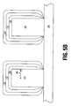
- Figure 1A shows a perspective view of a faceplate 100 of a flat panel display device having a matrix structure 102 coupled thereto.
- matrix structure 102 is located on faceplate 100 such that the row and columns of matrix structure 102 separate adjacent sub-pixel regions, typically shown as 104.
- matrix structure 102 is formed of polyimide material.
- matrix structure 102 is formed of polyimide material in the present example, the present invention is also well suited to use with various other matrix forming materials which may cause deleterious contamination.
- the present invention is also well suited for use with a matrix structure which is comprised of a photosensitive polyimide formulation containing components other than polyimide.
- matrix structure 102 is a "multi-level" matrix structure. That is, the rows of matrix structure 102 have a different height than the columns of matrix structure 102. Such a multi-level matrix structure is shown in Figure 1A in order to more clearly show sub-pixel regions 104.
- the present invention is, however, well suited to use with a matrix structure which is not multi-level.
- the matrix structure of the present invention is sometimes referred to as a black matrix, it will be understood that the term “black” refers to the opaque characteristic of the matrix structures. That is, the present invention is also well suited to having a color other than black.
- black refers to the opaque characteristic of the matrix structures. That is, the present invention is also well suited to having a color other than black.
- only a portion of the interior surface of a faceplate is shown for purposes of clarity.
- a contaminant prevention structure is also well suited for use with various other physical components of a flat panel display device.
- some embodiments of the present invention refer to a matrix structure for defining pixel and/or sub-pixel regions of the flat panel display, the present invention is also well suited to an embodiment in which the pixel/sub-pixel defining structure is not a "matrix" structure. Therefore, for purposes of the present application, the term matrix structure refers to a pixel and/or sub-pixel defining structure and not to a particular physical shape of the structure.
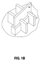
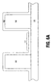
- FIG. 1B a perspective view of a support structure 150 adapted to be encapsulated by a contaminant prevention structure is shown.
- support structure 150 is encapsulated by a contaminant prevention structure. That is, the contaminant prevention structure has a physical structure such that contaminants originating within support structure 150 are confined within support structure 150. Thus, the contaminant prevention structure prevents contaminants which are generated within support structure 150 from migrating outside of support structure 150.
- the material comprising the contaminant prevention structure does not outgas contaminants when struck by electrons emitted from a cathode portion of the flat panel display.
- support structure 150 is a wall in Figure 1B
- the contaminant prevention structure is also well suited for pins, balls, columns, or various other supporting structures.
- FIG. 1C a side sectional view of a focus structure 160 adapted to be encapsulated by a contaminant prevention structure is shown.
- focus structure 160 is encapsulated by a contaminant prevention structure. That is, the contaminant prevention structure has a physical structure such that contaminants originating within focus structure 160 are confined within focus structure 160.
- the contaminant prevention structure prevents contaminants which are generated within focus structure 160 from migrating outside of focus structure 160.
- the material comprising the contaminant prevention structure does not outgas contaminants when struck by electrons emitted from a cathode portion of the flat panel display.
- focus structure 160 is a waffle-like structure in Figure 1C
- the contaminant prevention structure is also well suited to an example in which the focus structure has a different shape.
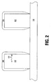
- FIG. 2 a side sectional view of faceplate 100 and matrix structure 102 taken along line A-A of Figure 1A is shown.
- the side sectional view only a portion of matrix structure 102 is shown for purposes of clarity. It will be understood, however, that the following steps are performed over a much larger portion of matrix structure 102 and are not limited only to those portion of matrix structure 102 shown in Figure 2 . Additionally, the following steps are also well suited to an approach in which a preliminary bake-out step is used to initially purge some of the contaminants from the matrix. In a bake-out step, the polyimide matrix is heated prior to placing the polyimide matrix in the sealed vacuum environment of the flat panel display.
- a contaminant prevention structure 106 is disposed covering matrix structure 102.
- contaminant prevention structure 106 is comprised of a layer of substantially non-porous material. That is, matrix structure 102 has a physical structure such that contaminants originating within matrix structure 102 are confined within matrix structure 102. Thus, contaminant prevention structure 106 prevents contaminants which are generated within matrix structure 102 from migrating outside of matrix structure 102. In addition to confining contaminants within matrix structure 102, the material comprising contaminant prevention structure 106 does not outgas contaminants when struck by electrons emitted from a cathode portion of the flat panel display.
- arrow 108 depicts the path of a contaminant generated within matrix structure 102. It will be understood that such contaminants include species such as, for example, N2, H2, CH 4 , CO, CO 2 O 2 , and H 2 O. As shown by arrow 108, contaminant prevention structure 106 prevents contaminants from being emitted from matrix structure 102.
- contaminant prevention structure 106 is comprised of a substantially non-porous material.
- the substantially non-porous material of contaminant prevention structure 106 is selected from the group consisting of silicon oxide, a metal film, an inorganic solid, and the like.
- the present example is also well suited to the use of material such as aluminum, beryllium, and chemical vapor deposited silicon oxide for non-porous prevention structure 106.
- the material of non-porous prevention structure 106 can be a solid with a melting point of greater than approximately 500 degrees Celsius.
- the substantially non-porous material is deposited over matrix structure 102 by chemical vapor deposition (CVD), evaporation, sputtering, or other means, to a thickness of approximately 500-5000 angstroms. It will be understood, however, that various other substantially non-porous materials are suited to confining contaminants within matrix structure 102. It is also possible to vary the thickness of contaminant prevention structure 106 to greater than or less than the thickness range listed above.
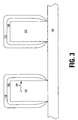
- a multi-layer contaminant prevention structure is disposed covering matrix structure 102.
- the multi-layer contaminant prevention structure is comprised of a plurality of layers, 106 and 110, of substantially non-porous material. That is, matrix structure 102 has a physical structure such that contaminants originating within matrix structure 102 are confined within matrix structure 102.
- the present multi-layer contaminant prevention structure prevents contaminants which are generated within matrix structure 102 from migrating outside of matrix structure 102.
- layers 106 and 110 do not outgas contaminants when struck by electrons emitted from a cathode portion of the flat panel display.
- arrow 108 depicts the path of a contaminant generated within matrix structure 102.
- contaminants include species such as, for example, N 2 , H 2 , CH 4 , CO, CO 2 , O 2 , and H 2 O.
- the present multi-layer contaminant prevention structure prevents contaminants from being emitted from matrix structure 102.
- multi-layer contaminant prevention structure is comprised of a plurality of layers of substantially non-porous material.
- at least one of the substantially non-porous layers of material, 106 and 110, of the multi-layer contaminant prevention structure is selected from the group consisting of: silicon dioxide; a metal film; an inorganic solid, and the like.
- the present example is also well suited to the use of material such as aluminum, beryllium, and chemical vapor deposited silicon oxide for at least one of the substantially non-porous layers of material 106 and 110.
- at least one of the non-porous layers of material 106 and 110 can be comprised of a solid with a melting point of greater than approximately 500 degrees Celsius.
- the multi-layer contaminant prevention structure has a total thickness of approximately 500-5000 angstroms. It will be understood, however, that various other substantially non-porous materials are suited to confining contaminants within matrix structure 102.
- the total thickness of the multi-layer contaminant prevention structure can be varied to greater than or less than the thickness range listed above. Furthermore, it is also possible to vary the number of layers of substantially non-porous material which comprise the multi-layer contaminant prevention structure.
- the multi-layer contaminant prevention structure has a thickness which is sufficient to prevent penetration by electrons directed towards faceplate 100.
- the multi-layer contaminant prevention structure includes a layer of silicon dioxide deposited covering matrix 102 by CVD to a thickness of approximately 1000-5000 angstroms.
- a contaminant prevention structure 112 is disposed covering matrix structure 102 and the sub-pixel regions 114 of faceplate 100.
- the substantially non-porous material is a transparent material such as silicon dioxide or indium tin oxide which is deposited over matrix structure 102 and sub-pixel regions 114 by chemical vapor deposition (CVD), evaporation, sputtering, or other means, to a thickness of approximately 500-5000 angstroms.
- CVD chemical vapor deposition
- evaporation evaporation, sputtering, or other means
- the contaminant prevention structure 112 has a thickness which is sufficient to prevent penetration by electrons directed towards faceplate 100.
- the present example confines thermally generated contaminants within matrix structure 102, and further prevents contaminants from being formed by electron stimulated desorption. That is, the present example substantially eliminates a major deleterious condition associated with electron bombardment of matrix structure 102.
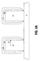
- conductive coating 116 is disposed covering a contaminant prevention structure 106.
- the present example depicts the example of Figure 2 , having conductive coating 116 disposed thereover.
- conductive coating is preferably comprised of a low atomic number material.
- a low atomic number material refers to a material comprised of elements having atomic numbers of less than 18. Additionally, a low atomic number material will reduce the electron scattering compared to a high atomic number material.
- conductive coating 116 is comprised, for example, of a CB800A DAG made by Acheson Colloids of Port Huron, Michigan.
- conductive coating 116 is comprised of a graphite-based conductive material.
- the layer of graphite-based conductive material is applied as a semi-dry spray to reduce shrinkage of conductive coating 116. Doing so, allows for improved control over the final depth of conductive coating 116.
- deposition methods are recited above, it will be understood that various other deposition methods are suited to deposit various other conductive coatings over contaminant prevention structure 106. For example, an aluminum coating which is applied by an angled evaporation can be used.
- the top surface of matrix structure 102 is physically closer to the field emitter than is faceplate 100.
- the present example provides a constant potential surface.
- the present example reduces the possibility of potential arcing.
- the present example helps to ensure that the integrity of the phosphors and the overlying aluminum layer (not yet deposited in Figure 5A ) is maintained.
- the conductive encapsulating layer can be made more electrically or thermally conductive than the aluminum layer over the phosphor by making it thicker or of a more conductive material, thereby enabling the encapsulating material to readily prevent localized voltage spikes by carrying offhigh electrical currents of potential arcs and to better physically withstand any arcs that may occur.
- the conductive coating can be a single layer (as in Figure 2 ) on the black matrix and need not be a double layer as drawn.
- conductive coating 116 is disposed covering layers 106 and 110 of a multi-layer contaminant prevention structure.
- conductive coating is preferably comprised of a low atomic number material, or a material comprised predominantly of low atomic number elements.
- a low atomic number material refers to a material comrised of elements having atomic numbers of less than 18.
- conductive coating 116 is comprised, for example, of a CB800A DAG made by Acheson Colloids of Port Huron, Michigan.
- conductive coating 116 is comprised of a graphite-based conductive material.
- the layer of graphite-based conductive material is applied as a semi-dry spray to reduce shrinkage of conductive coating 16. Doing so, allows for improved control over the final depth of conductive coating 116.
- deposition methods are recited above, it will be understood that various other deposition methods to deposit various other conductive coatings over layers 106 and 110 of the multi-layer contaminant prevention structure can be used.
- an aluminum coating which is applied by an angled evaporation can be used.
- the present example provides a constant potential surface and decreases the chances that any electrical arcing will occur. As result, the present example helps to ensure that the integrity of the phosphors and the overlying aluminum layer (not yet deposited in Figure 5B ) is maintained.
- conductive coating 116 is disposed over contaminant prevention structure 112.
- conductive coating is preferably comprised of a low atomic number material. More specifically, in one example, conductive coating 116 is comprised, for example, of a CB800A DAG made by Acheson Colloids of Port Huron, Michigan. In another example, conductive coating 116 is comprised of a graphite-based conductive material. In still another example, the layer of graphite-based conductive material is applied as a semi-dry spray to reduce shrinkage of conductive coating 116.
- conductive coating 116 allows for improved control over the final depth of conductive coating 116.
- deposition methods are recited above, it will be understood that various other deposition methods to deposit various other conductive coatings over contaminant prevention structure 112 can be used.
- an aluminum coating which is applied by an angled evaporation can be used.
- the present example provides a constant potential surface and decreases the chances that any electrical arcing will occur. As result, the present example helps to ensure that the integrity of the phosphors and the overlying aluminum layer (not yet deposited in Figure 5C ) is maintained.
- these example eliminate deleterious browning and outgassing associated with prior art polyimide based black matrix structures. Additionally, by preventing contaminants from being emitted by the matrix structure, the above example prevent coating of the field emitters by the released contaminants. Additionally, by reducing the number and energy of electrons striking the polyimide, electron desorption of contaminants is reduced. As a result, the above example extend the life of the field emitters. As yet an additional advantage, the contaminants prevention structure also protects the matrix structure from potential damage during subsequent processing steps, and electrical arcs.
- matrix structure 102 is formed of polyimide material in the present embodiment.
- the present invention as explained in the following embodiments is also well suited to use with various other matrix forming materials which may cause deleterious contamination.
- the present invention is also well suited for use with a matrix structure which is comprised of a photosensitive polyimide formulation containing components other than polyimide.
- a contaminant prevention structure is also well suited for use with various other physical components such as, for example, support structures and/or focus structures.
- a contaminant prevention structure 602 is disposed covering matrix structure 102 and the sub-pixel regions 114 of faceplate 100.
- contaminant prevention structure 602 extends into sub-pixel or pixel regions 114, the presence of the transparent porous or non-porous material in sub-pixel or pixel regions 114 does not adversely affect the formation or operation of the flat panel display. It will be understood, however, that the present invention is well suited to an embodiment in which the porous material of contaminant prevention structure 602 does not extend into sub pixel regions 114.
- contaminant prevention structure 606 is comprised of a layer of porous material.
- a contaminant prevention structure 602 comprising a layer of porous material prevents electrons and X-rays generated within the flat panel display from striking matrix structure 102. Additionally, the material of the contaminant prevention structure 602 of the present invention does not outgas contaminants when struck by electrons or X-rays generated within the flat panel display. It will be understood that such contaminants include species such as, for example, N 2 , H 2 , CH 4 , CO, CO 2 , O 2 , and H 2 O.
- the contaminant prevention structure 602 of the present invention as claimed comprises a porous material.
- the porous material of contaminant prevention structure 602 is selected from the group consisting of: colloidal silica, silicon oxide; and chemical vapor deposited silicon oxide. It will be understood, however, that the present invention is also well suited to use with various other porous materials such as, for example, silicon, oxides, nitrides, carbides, diamond, and the like. Moreover, the present invention is well suited to an embodiment in which the material of porous contaminant prevention structure 602 is a solid with a melting point of greater than approximately 500 degrees Celsius.
- the porous material is silicon dioxide which is deposited over matrix structure 102 by atmospheric pressure physical vapor deposition (APPVD) to a thickness of approximately 300-10,000 angstroms.
- ASVD atmospheric pressure physical vapor deposition
- the present invention is well suited to the use of various other porous materials which are suited to preventing electron and/or X-ray penetration therethrough by electrons and/or X-rays generated in the flat panel display.
- the present invention is also well suited to an embodiment in which the layer of porous material is applied, for example, by sputtering, e-beam evaporation, spraying methods, dip-coating methods, and the like.
- the present invention is also well suited to varying the thickness of contaminant prevention structure 602 to greater than or less than the thickness range listed above. More specifically, at 6 keV, the vast majority of electrons will not penetrate farther than 6000 angstroms into silicon dioxide. At 10 keV, the vast majority of electrons will not penetrate farther than 10,000 angstroms into silicon dioxide. Therefore, in the present embodiment, the depth of the porous material comprising contaminant prevention structure 602 is adjusted so as to ensure that matrix structure 102 is not bombarded by electrons and/or X-rays generated within the flat panel display.
- a multi-layer contaminant prevention structure is disposed covering matrix structure 102.
- the multi-layer contaminant prevention structure comprises plurality of layers, 602 and 604, of porous material.
- the present embodiment prevents electrons and X-rays generated within the flat panel display from striking matrix structure 102. Additionally, the material comprising the contaminant prevention structure of the present invention does not outgas contaminants when struck by electrons or X-rays generated within the flat panel display.
- multi-layer contaminant prevention structure comprises a plurality of layers of porous material.
- at least one of the layers of porous material, 602 and 604, of the multi-layer contaminant prevention structure is selected from the group consisting of: colloidal silica; silicon oxide; and chemical vapor deposited silicon oxide.
- colloidal silica silicon oxide
- silicon oxide silicon oxide
- chemical vapor deposited silicon oxide silicon oxide
- the present invention is also well suited to use with various other porous materials such as, for example, silicon, oxides, nitrides, carbides, graphite, aluminum, diamond, and the like.
- the present invention is well suited to an embodiment in which at least one of the layers of porous material 602 and 604 is a solid with a melting point of greater than approximately 500 degrees Celsius.
- the porous material of at least one of layers 602 and 604 is silicon dioxide which is deposited over matrix structure 102 by atmospheric pressure physical vapor deposition (APPVD) to a thickness of approximately 300-10,000 angstroms.
- APSVD atmospheric pressure physical vapor deposition
- the present invention is well suited to the use of various other porous materials which are suited to preventing electron and/or X-ray penetration therethrough by electrons and/or X-rays generated in the flat panel display.
- the present invention is also well suited to an embodiment in which the layer of porous material is applied, for example, by sputtering, e-beam evaporation, spraying methods, dip-coating methods, and the like.
- the present invention is also well suited to varying the thickness of contaminant prevention structure to greater than or less than the thickness range listed above.
- the combined depth of the layers of porous material 602 and 604 comprising the contaminant prevention structure is adjusted so as to ensure that matrix structure 102 is not bombarded by electrons and/or X-rays generated within the flat panel display.
- conductive coating 606 is disposed over a contaminant prevention structure.
- the present embodiment depicts the embodiment of Figure 6B having conductive coating 606 disposed thereover.
- the present invention is, however, well suited to an embodiment in which conductive coating 606 is disposed over, for example, the embodiment of Figure 6A .
- conductive coating preferably comprises a low atomic number material. More specifically, in one embodiment, conductive coating 606 comprises, for example, a CB800A DAG made by Acheson Colloids of Port Huron, Michigan. In another embodiment, conductive coating 606 comprises a graphite-based conductive material.
- the layer of graphite-based conductive material is applied as a semi-dry spray to reduce shrinkage of conductive coating 606.
- the present invention allows for improved control over the final depth of conductive coating 606.
- conductive coating 606 is deposited to a depth of 1000-5000 angstroms.
- the present embodiment provides a constant potential surface and decreases the chances that any electrical arcing will occur. As result, the present embodiment helps to ensure that the integrity of the phosphors and the overlying aluminum layer (not yet deposited in the embodiment of Figure 6C ) is maintained.
- a multi-layer contaminant prevention structure is disposed covering matrix structure 102.
- the multi-layer contaminant prevention structure comprises a plurality of layers, 702 and 704.
- layer 702 comprises a porous material
- layer 704 comprises a layer of substantially non-porous material.
- the present embodiment prevents electrons and X-rays generated within the flat panel display from striking matrix structure 102. This embodiment further confines thermally generated contaminants within matrix structure 102.
- the material comprising the contaminant prevention structure of the present invention does not outgas contaminants when struck by electrons or X-rays generated within the flat panel display.
- the multi-layer contaminant prevention structure comprises a plurality of layers of material.
- porous material, 702 of the multi-layer contaminant prevention structure is selected from the group consisting of: colloidal silica; silicon oxide; and chemical vapor deposited silicon oxyde. It will be understood, however, that the present invention is also well suited to use with various other porous materials such as, for example, silicon, oxides, nitrides, carbides, diamond, and the like. Moreover, the present invention is well suited to an embodiment in which at least one of the layers of material 702 and 704 is a solid with a melting point of greater than approximately 500 degrees Celsius.
- the plurality of layers of material are defined as follows.
- Layer 702 comprises a layer of indium tin oxide which is deposited to a depth of approximately 1000-10,000 angstroms.
- Layer 704 comprises a silicon oxide which is deposited over matrix structure 102 to a thickness of approximately 300-10,000 angstroms. It will be understood, however, that the present invention is well suited to the use of various other porous and non-porous materials. The present invention is also well suited to an embodiment in which the layer of porous material is applied, for example, by sputtering, e-beam evaporation, spraying methods, dip-coating methods, and the like.
- the present invention is also well suited to varying the thickness of the contaminant prevention structure to greater than or less than the thickness range listed above.
- the combined depth of the layers of material 702 and 704 comprising the contaminant prevention structure is adjusted so as to ensure that matrix structure 102 is not bombarded by electrons and/or X-rays generated within the flat panel display.
- a conductive coating 706 is disposed over a contaminant prevention structure.
- the present embodiment depicts the embodiment of Figure 7A having conductive coating 706 disposed thereover.
- layer 702 is comprised of a layer of indium tin oxide which is deposited to a depth of approximately 1000-10,000 angstroms.
- layer 704 is comprised of a silicon oxide which is deposited over matrix structure 102 to a thickness of approximately 300-10,000 angstroms.
- Layer 706 of this embodiment is comprised of a layer of aluminum which is deposited to a depth of approximately 300-2000 angstroms.
- the conductive coating preferably comprises a low atomic number material.
- conductive coating 706 comprises for example, a CB800A DAG made by Acheson Colloids of Port Huron, Michigan.
- conductive coating 706 comprises a graphite-based conductive material.
- the layer of graphite-based conductive material is applied as a semi-dry spray to reduce shrinkage of conductive coating 706.
- the present invention allows for improved control over the final depth of conductive coating 706.
- the contaminant structure comprises two distinct layers of material 702 and 704.
- the contaminant prevention structure comprises a layer of porous material (e.g. layer 704 of silicon oxide) having non-porous material (e.g. the indium tin oxide of layer 702) impregnated therein.
- the present invention is also well suited to an embodiment in which a layer of substantially porous material has substantially non-porous material impregnated therein.
- the layer of substantially porous material is deposited as is described above in detail.
- substantially non-porous material is impregnated within the layer of substantially non-porous material by, for example, sputtering, physical vapor deposition, and the like.
- present embodiment is also well suited to having a conductive coating disposed thereover as is describe above in great detail.
- matrix structure 102 is formed of polyimide material in the present example.
- Various other matrix forming materials can be user which may cause deleterious contamination,
- a matrix structure can be comprised of a photosensitive polyimide formulation containing components other than polyimide.
- a contaminant prevention structure is also well suited for use with various other physical components such as, for example, support structures and/or focus structures.
- contaminant prevention structure 802 is disposed over matrix structure 102 and into sub-pixel regions 114.
- Contaminant prevention structure 802 further includes a dye (typically shown as dye particles 804).
- contaminant prevention structure 802 is comprised of silicon oxide doped with dye material.
- the present example provides a color filter which enhances display contrast by reducing reflected ambient light.
- the present example is well suited to having the dye disposed only in those portions of contaminant prevention structure 802 which reside above sub-pixel regions 114.
- the present example is also well suited to having the dye disposed in the entire contaminant prevention structure 802.
- the present example provides a constant potential surface and decreases the chances that any electrical arcing will occur. As result, the present example helps to ensure that the integrity of the phosphors and the overlying aluminum layer (not yet deposited in the example of Figure 8 is maintained.
- the present invention provides a matrix structure which does not deleteriously outgas when subjected to thermal variations.
- the present invention also provides an embodiment in which a matrix structure meets the above-listed need and which reduces unwanted electron stimulated desorption of contaminants.
- the present invention provides a matrix structure which meets both of the above needs and which also achieves electrical robustness in the faceplate by providing a constant potential surface which reduces the possibility of potential arcing.
- the conductive matrix structure of the present invention is applicable in numerous types of flat panel displays.
Landscapes
- Cathode-Ray Tubes And Fluorescent Screens For Display (AREA)
Applications Claiming Priority (3)
| Application Number | Priority Date | Filing Date | Title |
|---|---|---|---|
| US09/087,785 US6215241B1 (en) | 1998-05-29 | 1998-05-29 | Flat panel display with encapsulated matrix structure |
| PCT/US1999/011170 WO1999063567A1 (en) | 1998-05-29 | 1999-05-20 | Display with encapsulated matrix structure |
| US87785 | 2008-08-11 |
Publications (3)
| Publication Number | Publication Date |
|---|---|
| EP1082744A1 EP1082744A1 (en) | 2001-03-14 |
| EP1082744A4 EP1082744A4 (en) | 2004-05-12 |
| EP1082744B1 true EP1082744B1 (en) | 2009-12-09 |
Family
ID=22207245
Family Applications (1)
| Application Number | Title | Priority Date | Filing Date |
|---|---|---|---|
| EP99925701A Expired - Lifetime EP1082744B1 (en) | 1998-05-29 | 1999-05-20 | Display with encapsulated matrix structure |
Country Status (6)
| Country | Link |
|---|---|
| US (2) | US6215241B1 (enExample) |
| EP (1) | EP1082744B1 (enExample) |
| JP (1) | JP4577986B2 (enExample) |
| KR (1) | KR100766887B1 (enExample) |
| DE (1) | DE69941780D1 (enExample) |
| WO (1) | WO1999063567A1 (enExample) |
Families Citing this family (17)
| Publication number | Priority date | Publication date | Assignee | Title |
|---|---|---|---|---|
| US7002287B1 (en) * | 1998-05-29 | 2006-02-21 | Candescent Intellectual Property Services, Inc. | Protected substrate structure for a field emission display device |
| US6353286B1 (en) * | 1999-10-08 | 2002-03-05 | Motorola, Inc | Field emission display having a multi-layered barrier structure |
| US6410101B1 (en) * | 2000-02-16 | 2002-06-25 | Motorola, Inc. | Method for scrubbing and passivating a surface of a field emission display |
| US6432593B1 (en) * | 2000-05-31 | 2002-08-13 | Candescent Technologies Corporation | Gripping multi-level structure |
| WO2002011169A1 (en) * | 2000-07-28 | 2002-02-07 | Candescent Technologies Corporation | Protected structure of flat panel display |
| US7315115B1 (en) | 2000-10-27 | 2008-01-01 | Canon Kabushiki Kaisha | Light-emitting and electron-emitting devices having getter regions |
| US6992322B2 (en) * | 2001-01-02 | 2006-01-31 | Kavassery Sureswaran Narayan | Photo-responsive organic field effect transistor |
| US6812636B2 (en) | 2001-03-30 | 2004-11-02 | Candescent Technologies Corporation | Light-emitting device having light-emissive particles partially coated with light-reflective or/and getter material |
| US6743068B2 (en) * | 2001-03-31 | 2004-06-01 | Sony Corporation | Desorption processing for flat panel display |
| US6784610B2 (en) * | 2002-08-29 | 2004-08-31 | Alan D. Ellis | Display panel apparatus and method |
| TW574448B (en) * | 2002-09-24 | 2004-02-01 | Au Optronics Corp | Method for fabricating a polysilicon layer |
| KR100496286B1 (ko) * | 2003-04-12 | 2005-06-17 | 삼성에스디아이 주식회사 | 유기 전계 발광 표시 장치 및 이의 제조 방법 |
| TW200614411A (en) * | 2004-09-04 | 2006-05-01 | Applied Materials Inc | Substrate carrier having reduced height |
| CN2788876Y (zh) * | 2005-05-10 | 2006-06-21 | 张逸夫 | 模拟花开动作的仿真玩具花 |
| US20070116545A1 (en) * | 2005-11-21 | 2007-05-24 | Applied Materials, Inc. | Apparatus and methods for a substrate carrier having an inflatable seal |
| US20070141280A1 (en) * | 2005-12-16 | 2007-06-21 | Applied Materials, Inc. | Substrate carrier having an interior lining |
| US20080018218A1 (en) * | 2006-07-24 | 2008-01-24 | Wei-Sheng Hsu | Straddling and supporting structure for a field emission display device and a manufacturing method thereof |
Family Cites Families (18)
| Publication number | Priority date | Publication date | Assignee | Title |
|---|---|---|---|---|
| US5614781A (en) * | 1992-04-10 | 1997-03-25 | Candescent Technologies Corporation | Structure and operation of high voltage supports |
| US4923421A (en) * | 1988-07-06 | 1990-05-08 | Innovative Display Development Partners | Method for providing polyimide spacers in a field emission panel display |
| US5063327A (en) * | 1988-07-06 | 1991-11-05 | Coloray Display Corporation | Field emission cathode based flat panel display having polyimide spacers |
| NL9100122A (nl) * | 1991-01-25 | 1992-08-17 | Philips Nv | Weergeefinrichting. |
| FR2678424A1 (fr) | 1991-06-27 | 1992-12-31 | Thomson Tubes Electroniques | Elements electriquement isolants pour panneaux a plasma et procede pour la realisation de tels elements. |
| EP0546198B1 (en) * | 1991-06-28 | 1999-08-18 | Dai Nippon Printing Co., Ltd. | Black matrix base board and manufacturing method therefor, and liquid crystal display panel and manufacturing method therefor |
| EP0683920B2 (en) * | 1993-02-01 | 2006-04-12 | Candescent Intellectual Property Services, Inc. | Flat panel device with internal support structure |
| US5528103A (en) * | 1994-01-31 | 1996-06-18 | Silicon Video Corporation | Field emitter with focusing ridges situated to sides of gate |
| ATE237869T1 (de) * | 1994-11-21 | 2003-05-15 | Candescent Tech Corp | Feldemissionsvorrichtung mit innerem struktur zum ausrichten von phosphor-pixeln auf entsprechenden feldemittern |
| US5650690A (en) * | 1994-11-21 | 1997-07-22 | Candescent Technologies, Inc. | Backplate of field emission device with self aligned focus structure and spacer wall locators |
| GB9502435D0 (en) * | 1995-02-08 | 1995-03-29 | Smiths Industries Plc | Displays |
| JP3163563B2 (ja) * | 1995-08-25 | 2001-05-08 | 富士通株式会社 | 面放電型プラズマ・ディスプレイ・パネル及びその製造方法 |
| JPH09134686A (ja) * | 1995-11-11 | 1997-05-20 | Dainippon Printing Co Ltd | 画像表示装置 |
| EP0811219B1 (en) * | 1995-12-18 | 2001-10-04 | Koninklijke Philips Electronics N.V. | Channel plate with organic-walled plasma channels for a plasma addressed display device and a method for making such a plate |
| JP3171785B2 (ja) * | 1996-06-20 | 2001-06-04 | 富士通株式会社 | 薄型表示装置、及びそれに用いる電界放出陰極の製造方法 |
| EP0851458A1 (en) * | 1996-12-26 | 1998-07-01 | Canon Kabushiki Kaisha | A spacer and an image-forming apparatus, and a manufacturing method thereof |
| US5912056A (en) * | 1997-03-31 | 1999-06-15 | Candescent Technologies Corporation | Black matrix with conductive coating |
| US6051937A (en) * | 1998-05-29 | 2000-04-18 | Candescent Technologies Corporation | Voltage ratio regulator circuit for a spacer electrode of a flat panel display screen |
-
1998
- 1998-05-29 US US09/087,785 patent/US6215241B1/en not_active Expired - Lifetime
-
1999
- 1999-05-20 JP JP2000552698A patent/JP4577986B2/ja not_active Expired - Fee Related
- 1999-05-20 KR KR1020007013018A patent/KR100766887B1/ko not_active Expired - Fee Related
- 1999-05-20 WO PCT/US1999/011170 patent/WO1999063567A1/en not_active Ceased
- 1999-05-20 DE DE69941780T patent/DE69941780D1/de not_active Expired - Lifetime
- 1999-05-20 EP EP99925701A patent/EP1082744B1/en not_active Expired - Lifetime
-
2000
- 2000-02-29 US US09/505,823 patent/US6380670B1/en not_active Expired - Lifetime
Also Published As
| Publication number | Publication date |
|---|---|
| KR100766887B1 (ko) | 2007-10-15 |
| US6380670B1 (en) | 2002-04-30 |
| KR20010025059A (ko) | 2001-03-26 |
| US6215241B1 (en) | 2001-04-10 |
| EP1082744A1 (en) | 2001-03-14 |
| WO1999063567A1 (en) | 1999-12-09 |
| DE69941780D1 (de) | 2010-01-21 |
| JP4577986B2 (ja) | 2010-11-10 |
| EP1082744A4 (en) | 2004-05-12 |
| JP2002517882A (ja) | 2002-06-18 |
Similar Documents
| Publication | Publication Date | Title |
|---|---|---|
| US6853129B1 (en) | Protected substrate structure for a field emission display device | |
| EP1082744B1 (en) | Display with encapsulated matrix structure | |
| US6630786B2 (en) | Light-emitting device having light-reflective layer formed with, or/and adjacent to, material that enhances device performance | |
| EP0847589B1 (en) | Field emission display device with focusing electrodes at the anode and method for constructing same | |
| US5684356A (en) | Hydrogen-rich, low dielectric constant gate insulator for field emission device | |
| US5866978A (en) | Matrix getter for residual gas in vacuum sealed panels | |
| US6417605B1 (en) | Method of preventing junction leakage in field emission devices | |
| US6353286B1 (en) | Field emission display having a multi-layered barrier structure | |
| US6670753B1 (en) | Flat panel display with gettering material having potential of base, gate or focus plate | |
| US5717286A (en) | Electron excited luminous element with an anode substrate having a glass exposed subface provided with a hydrophobic property | |
| US7002287B1 (en) | Protected substrate structure for a field emission display device | |
| US6302757B1 (en) | Low-voltage cathode for scrubbing cathodoluminescent layers for field emission displays and method | |
| US7550913B2 (en) | Field emission device having getter material | |
| CN100341102C (zh) | 电子发射装置 | |
| KR100845433B1 (ko) | 평판 디스플레이의 보호 구조 | |
| US6398607B1 (en) | Tailored spacer structure coating | |
| US6692323B1 (en) | Structure and method to enhance field emission in field emitter device | |
| US6743068B2 (en) | Desorption processing for flat panel display | |
| US20060238457A1 (en) | Field emitter devices with emitters having implanted layer | |
| US20060232190A1 (en) | Electron emission device and method for manufacturing the same |
Legal Events
| Date | Code | Title | Description |
|---|---|---|---|
| PUAI | Public reference made under article 153(3) epc to a published international application that has entered the european phase |
Free format text: ORIGINAL CODE: 0009012 |
|
| 17P | Request for examination filed |
Effective date: 20001222 |
|
| AK | Designated contracting states |
Kind code of ref document: A1 Designated state(s): DE FR GB IE NL |
|
| 111L | Licence recorded |
Free format text: 0100 U.S. FEERAL GOVERNMENT Effective date: 20030324 |
|
| A4 | Supplementary search report drawn up and despatched |
Effective date: 20040330 |
|
| RIC1 | Information provided on ipc code assigned before grant |
Ipc: 7H 01J 31/12 B Ipc: 7H 01J 29/02 B Ipc: 7H 01J 5/08 B Ipc: 7H 01J 5/48 A |
|
| 17Q | First examination report despatched |
Effective date: 20040701 |
|
| RAP1 | Party data changed (applicant data changed or rights of an application transferred) |
Owner name: CANON KABUSHIKI KAISHA |
|
| GRAP | Despatch of communication of intention to grant a patent |
Free format text: ORIGINAL CODE: EPIDOSNIGR1 |
|
| GRAS | Grant fee paid |
Free format text: ORIGINAL CODE: EPIDOSNIGR3 |
|
| GRAA | (expected) grant |
Free format text: ORIGINAL CODE: 0009210 |
|
| AK | Designated contracting states |
Kind code of ref document: B1 Designated state(s): DE FR GB IE NL |
|
| REG | Reference to a national code |
Ref country code: GB Ref legal event code: FG4D |
|
| REG | Reference to a national code |
Ref country code: IE Ref legal event code: FG4D |
|
| REF | Corresponds to: |
Ref document number: 69941780 Country of ref document: DE Date of ref document: 20100121 Kind code of ref document: P |
|
| REG | Reference to a national code |
Ref country code: NL Ref legal event code: VDEP Effective date: 20091209 |
|
| PG25 | Lapsed in a contracting state [announced via postgrant information from national office to epo] |
Ref country code: NL Free format text: LAPSE BECAUSE OF FAILURE TO SUBMIT A TRANSLATION OF THE DESCRIPTION OR TO PAY THE FEE WITHIN THE PRESCRIBED TIME-LIMIT Effective date: 20091209 |
|
| PLBE | No opposition filed within time limit |
Free format text: ORIGINAL CODE: 0009261 |
|
| STAA | Information on the status of an ep patent application or granted ep patent |
Free format text: STATUS: NO OPPOSITION FILED WITHIN TIME LIMIT |
|
| 26N | No opposition filed |
Effective date: 20100910 |
|
| PG25 | Lapsed in a contracting state [announced via postgrant information from national office to epo] |
Ref country code: IE Free format text: LAPSE BECAUSE OF NON-PAYMENT OF DUE FEES Effective date: 20100520 |
|
| PGFP | Annual fee paid to national office [announced via postgrant information from national office to epo] |
Ref country code: DE Payment date: 20130531 Year of fee payment: 15 Ref country code: GB Payment date: 20130523 Year of fee payment: 15 |
|
| PGFP | Annual fee paid to national office [announced via postgrant information from national office to epo] |
Ref country code: FR Payment date: 20130621 Year of fee payment: 15 |
|
| REG | Reference to a national code |
Ref country code: DE Ref legal event code: R082 Ref document number: 69941780 Country of ref document: DE Representative=s name: WESER & KOLLEGEN, DE |
|
| REG | Reference to a national code |
Ref country code: DE Ref legal event code: R119 Ref document number: 69941780 Country of ref document: DE |
|
| GBPC | Gb: european patent ceased through non-payment of renewal fee |
Effective date: 20140520 |
|
| REG | Reference to a national code |
Ref country code: DE Ref legal event code: R119 Ref document number: 69941780 Country of ref document: DE Effective date: 20141202 |
|
| REG | Reference to a national code |
Ref country code: FR Ref legal event code: ST Effective date: 20150130 |
|
| PG25 | Lapsed in a contracting state [announced via postgrant information from national office to epo] |
Ref country code: DE Free format text: LAPSE BECAUSE OF NON-PAYMENT OF DUE FEES Effective date: 20141202 |
|
| PG25 | Lapsed in a contracting state [announced via postgrant information from national office to epo] |
Ref country code: FR Free format text: LAPSE BECAUSE OF NON-PAYMENT OF DUE FEES Effective date: 20140602 Ref country code: GB Free format text: LAPSE BECAUSE OF NON-PAYMENT OF DUE FEES Effective date: 20140520 |