EP1081940A1 - Synchronous processing circuit - Google Patents
Synchronous processing circuit Download PDFInfo
- Publication number
- EP1081940A1 EP1081940A1 EP00901924A EP00901924A EP1081940A1 EP 1081940 A1 EP1081940 A1 EP 1081940A1 EP 00901924 A EP00901924 A EP 00901924A EP 00901924 A EP00901924 A EP 00901924A EP 1081940 A1 EP1081940 A1 EP 1081940A1
- Authority
- EP
- European Patent Office
- Prior art keywords
- signal
- phase
- synchronizing signal
- vertical
- pulse width
- Prior art date
- Legal status (The legal status is an assumption and is not a legal conclusion. Google has not performed a legal analysis and makes no representation as to the accuracy of the status listed.)
- Withdrawn
Links
Images










Classifications
-
- H—ELECTRICITY
- H04—ELECTRIC COMMUNICATION TECHNIQUE
- H04N—PICTORIAL COMMUNICATION, e.g. TELEVISION
- H04N5/00—Details of television systems
- H04N5/04—Synchronising
- H04N5/08—Separation of synchronising signals from picture signals
-
- H—ELECTRICITY
- H04—ELECTRIC COMMUNICATION TECHNIQUE
- H04N—PICTORIAL COMMUNICATION, e.g. TELEVISION
- H04N5/00—Details of television systems
- H04N5/04—Synchronising
- H04N5/06—Generation of synchronising signals
-
- H—ELECTRICITY
- H04—ELECTRIC COMMUNICATION TECHNIQUE
- H04N—PICTORIAL COMMUNICATION, e.g. TELEVISION
- H04N5/00—Details of television systems
- H04N5/04—Synchronising
- H04N5/08—Separation of synchronising signals from picture signals
- H04N5/10—Separation of line synchronising signal from frame synchronising signal or vice versa
Definitions
- the present invention relates to synchronous processor circuits in a color receiver and, more specifically, to a synchronous processor circuit for reproducing a synchronizing signal externally provided by a video signal source to a color receiver, and supplying the synchronizing signal to each circuit block in the color receiver.
- FIG. 14 is a block diagram showing the structure of a conventional synchronous processor circuit.
- the synchronous processor circuit includes an LPF 1 to which a composite signal 5 is externally provided, and a vertical synchronization separating signal 6 is separated therefrom and outputted; a phase delay part 2 for receiving the composite signal 5 and outputting a plurality of horizontal synchronizing signals 19 to 24 each differently delayed in phase; and a vertical synchronizing signal reproduction circuit 3 for receiving the plurality of horizontal synchronizing signals 19 to 24 each differently delayed in phase and the vertical synchronization separating signal 6 and outputting a vertical synchronizing signal 8.
- the phase delay part 2 includes first to sixth phase delay circuits 201 to 206.
- the LPF is a low pass filter. The operation of this synchronous processor circuit is described next below.
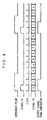
- FIG. 15 is a time chart which explains the operation of the conventional synchronous processor circuit.
- t1 to t13 indicate time at a regular interval.
- time t1 to time t13 indicate timing for a horizontal synchronizing signal to rise.
- the composite signal 5 externally provided to a display is a synchronizing signal onto which a vertical synchronizing signal and a horizontal synchronizing signal are superimposed.
- the horizontal synchronizing signal is a pulse signal which rises every time at times t1 to time t13.
- the vertical synchronizing signal is a pulse signal which rises at time t4 and falls at time t8.
- the composite signal 5 is also provided to each of the first to sixth phase delay circuits 201 to 206 in the phase delay part 2. Those inputted composite signals 5 each generate a pulse corresponding to a period of the horizontal synchronizing signal. By using the pulses corresponding to the period of the horizontal synchronizing signal, the first to sixth phase delay circuits 201 to 206 output horizontal synchronizing signals 19 to 24 varied in phase with a predetermined interval in the corresponding phase delay circuit, respectively.
- the horizontal synchronizing signals 19 to 24 phase-delayed as such and the vertical synchronization separating signal 6 are provided to the vertical synchronizing signal reproduction circuit 3.
- the vertical synchronizing signal reproduction circuit 3 outputs the vertical synchronizing signal 8 having the phase relationship with the horizontal synchronizing signal determined.
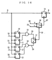
- FIG. 16 is a diagram showing an exemplary detailed structure of the vertical synchronizing signal reproduction circuit 3.
- the vertical synchronizing signal reproduction circuit 3 includes flip-flops 10 to 13, each of which receives the phase-delayed horizontal synchronizing signal 19, 21, 22, or 24 and the vertical synchronization separating signal 6; a NAND gate 15 which receives signals from the flip-flops 10 and 11; a NAND gate 16 which receives signals from the flip-flops 12 and 13; a set-reset flip-flop 17 in which a signal from the NAND gate 15 goes to the set and a signal from the NAND gate 16 to the reset; a multiplexer 18 which receives a signal from the set-reset flip-flop 17 as a control signal and the phase-delayed horizontal synchronizing signals 20 and 23, and outputs a signal 27 which is either one of the horizontal synchronizing signals; and a flip-flop 10 which receives the vertical synchronization separating signal
- the flip-flop 10 plays a role as latch means for latching a vertical synchronization separating signal, and outputting a synchronizing signal having the phase relationship with the horizontal synchronizing signal determined.
- the multiplexer 18 plays a role as signal selection means for selecting, for output, a signal for latching the vertical synchronization separating signal from among a plurality of phase-delayed signals.
- the flip-flops 10 to 13, the NAND gates 15 and 16, and the set-reset flip-flop 17 play a role as signal selection control means for outputting a signal to control the multiplexer 18 which phase-delayed signal is selected therein.
- the operation of such structured vertical synchronizing signal reproduction circuit 3 is described next below by referring to FIGS. 16 and 17.
- FIG. 17 is a time chart showing the operation of the vertical synchronizing signal reproduction circuit 3 from time t4 to time t5 in FIG. 15.
- a timing (denoted by time tA in the drawing) which coincides with a threshold value between a high level and a low level of the vertical synchronization separating signal 6 is observed between timings for the phase-delayed synchronizing signals 19 and 21 to rise.
- the output signal from the NAND gate 15 changes in level from high to low with the timing when the phase-delayed horizontal synchronizing signal 21 rises.
- the signal is a set incoming signal 25 which is inputted into the set terminal of the set-reset flip-flop 17.
- an output signal 33 from the set-reset flip-flop 17 is fixed in the low level.
- the output signal 33 from the set-reset flip-flop 17 is provided to a control terminal of the multiplexer 18.
- the multiplexer 18 When receiving a signal high in level in the control terminal, the multiplexer 18 selects the phase-delayed horizontal synchronizing signal 20 for output. When a signal low in level is inputted thereto, the multiplexer 18 selects the phase-delayed horizontal synchronizing signal 23 for output. Accordingly, the multiplexer 18 having the signal low in level provided to its control terminal selects and outputs the phase-delayed horizontal synchronizing signal 23.
- the phase-delayed horizontal synchronizing signal 23 can assuredly be latched with the vertical synchronization separating signal 6 with the timing which coincides with the threshold value between the high level and low level thereof. This is because, as described in the foregoing, the timing which coincides with the threshold value between the high level and the low level of the vertical synchronization separating signal 6 is observed between the timings for the phase-delayed horizontal synchronizing signals 19 and 21 to rise. Therefore, it is not certain whether the phase-delayed horizontal synchronizing signal 20 between the phase-delayed horizontal synchronizing signals 19 and 21 is capable for latching. Accordingly, the flip-flop 14 can assuredly latch the vertical synchronization separating signal 6 with the help of the phase-delayed horizontal synchronizing signal 23.
- the timing which coincides with the threshold value between the high level and the low level of the vertical synchronization separating signal 6 is observed between the phase-delayed horizontal synchronizing signals 19 arid 21.
- the timing which coincides with the threshold value between the high level and the low level of the vertical synchronization separating signal 6 may be observed between the timings for the phase-delayed horizontal synchronizing signals 22 and 24 to rise.
- the multiplexer 18 selects, for output, not the phase-delayed horizontal synchronizing signal 23 but the phase-delayed horizontal synchronizing signal 20. Accordingly, similar to the above-described case, the flip-flop 14 can assuredly latch the vertical synchronization separating signal 6.
- the vertical synchronizing signal reproduction circuit 3 can determine the phase relationship between the vertical synchronizing signal and the horizontal synchronization signals. As such, the vertical synchronizing signal reproduction circuit 3 can assuredly latch the vertical synchronization separating signal 6, and thus can supply, to each digital signal processor circuit arranged in the display, the vertical synchronizing signal 8 which has been accurately reproduced.
- FIGS. 18 are diagrams schematically showing a partially-enlarged waveform of the vertical synchronization separating signal 6.
- a dotted line laterally drawn in the drawings indicates the threshold value between the high level and the low level of the vertical synchronization separating signal 6.
- the threshold value is used by the flip-flops 10 to 14 which receive the vertical synchronization separating signal 6 to distinguish the level thereof between high and low.
- FIG. 18(a) is the diagram schematically showing the waveform at a front part of the vertical synchronization separating signal 6 in the range between time t4 and time t5 in FIG. 11.
- tA indicates a time when the vertical synchronization separating signal 6 reaches the threshold value as in FIG. 17.
- Ts indicates a period between time t4 and time tA.
- FIG. 18(b) is the diagram schematically showing the waveform at a rear part of the vertical synchronization separating signal 6 in the range between time t8 and time t9 in FIG. 11.
- tB indicates a time when the vertical synchronization separating signal 6 reaches the threshold value.
- Te indicates a period between time t8 and time tB.
- the waveform of the vertical synchronization separating signal 6 often differs in shape between the front part and the rear part, and the timings tA and tB which coincide with the threshold value between the high level and the low level of the vertical synchronization separating signal 6 often differ between the front part and the rear part thereof. Therefore, at the rear part of the vertical synchronization separating signal 6, unlike the above-described case in FIG. 17, the timing which coincides with the threshold value between the high level and the low level of the vertical synchronization separating signal 6 may be observed between the timings for the phase-delayed horizontal synchronizing signals 22 and 24 to rise.
- the multiplexer 18 may select, for output, the phase-delayed horizontal synchronizing signal 20, or the phase-delayed horizontal synchronizing signal 23. Consequently, the output signal 27 from the multiplexer 18 fails to be constant in horizontal synchronizing frequency as shown in FIG. 15. As such, according to the conventional structure, the phase relationship between the vertical synchronization separating signal 6 and the horizontal synchronizing signal is not determined. Therefore, the vertical synchronization signal provided therefrom cannot be stabilized enough.
- the LPF 1 is fixed in cutoff frequency. Therefore, the cutoff frequency of the LPF 1 may be too heavy (too low) for the vertical synchronizing signal component superimposed on the composite signal 5 depending on its pulse width. If this is the case, the vertical synchronization separating signal 6 provided by the LPF 1 may get very blunt. As exemplarily shown in FIG. 18, the vertical synchronization separating signal 6 provided by the LPF 1 shows a gradual change from time t4 to time t5, or from time t4 and time t5.
- the timings which coincide with the threshold value between the high level and the low level of the vertical synchronization separating signal 6 approximately coincide with both pulse timings of the above-described phase-delayed horizontal synchronizing signals 20 and 23, thereby causing such problem as above-described.
- an object of the present invention is to provide a synchronous processor circuit capable of improving a display's synchronization stability by determining a phase relationship between a vertical synchronizing signal and horizontal synchronizing signals, and circuitry structure of which can be simplified by setting a pulse width of the vertical synchronizing signal to be the integral multiple of the frequency of the horizontal synchronizing signal.
- a first aspect of the present invention is directed to a synchronous processor circuit arranged in a display for reproducing a synchronizing signal from a composite signal provided by a video signal source for stabilizing synchronization in the display, the circuit comprising:
- the stabilized vertical synchronizing signal can be supplied to each circuit arranged in the display.
- the frequency divider circuit outputs the vertical phase detection signal obtained by dividing the cycle of the vertical synchronizing signal into 1/2.
- the stabilized vertical synchronizing signal can be supplied to each circuit arranged in the display.
- the vertical synchronizing signal reproduction circuit comprises:
- the phase relationship between the vertical synchronizing signal and the horizontal synchronizing signal can be determined with the help of a plurality of phase-delayed signals inputted as signals for detecting a timing which coincides with the threshold value between the high level and the low level of the vertical synchronization separating signal.
- the synchronous processor circuit further comprises a pulse width reproduction circuit for receiving the signal from the vertical synchronizing signal reproduction circuit, and reproducing the synchronizing signal having a predetermined pulse width.
- the stabilized vertical synchronizing signal can be outputted with the counting operation carried out according to the set pulse width.
- the pulse width reproduction circuit comprises:
- the pulse width reproduction circuit can output the stabilized signal according to the pulse width which is previously set or calculated by operation.
- a sixth aspect of the present invention is directed to a synchronous processor circuit arranged in a display for reproducing a synchronizing signal from a composite signal provided by a video signal source for stabilizing synchronization in the display, the circuit comprising:
- the vertical synchronizing signal having the pulse width of the integral multiple of that of the frequency of the horizontal synchronizing signal with a structurally simplified circuit. Accordingly, the synchronous processor circuit in the display can be simplified in structure.
- the vertical synchronizing signal reproduction circuit comprises:
- the phase relationship between the vertical synchronizing signal and the horizontal synchronizing signal can be determined with the help of a plurality of phase-delayed signals inputted as signals for detecting a timing which coincides with the threshold value between the high level and the low level of the vertical synchronization separating signal.
- the synchronous processor circuit further comprises a pulse width reproduction circuit for receiving the signal from the flip-flop, and reproducing the synchronizing signal having a predetermined pulse width.
- the stabilized vertical synchronizing signal can be outputted with the counting operation carried out according to the set pulse width. Therefore, with a structurally simplified circuit, even with respect to the interlace signal, the vertical synchronizing signal can have the pulse width of the integral multiple of the frequency of the horizontal synchronizing signal. Therefore, it becomes possible to simplify the synchronous processor circuit in the display.
- the pulse width reproduction circuit comprises:
- the pulse width reproduction circuit can output the stabilized signal according to the pulse width which is previously set or calculated by operation.
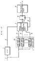
- FIG. 1 is a block diagram showing the structure of a synchronous processor circuit according to a first embodiment of the present invention.
- the synchronous processor circuit includes the LPF 1 to which the composite signal 5 is externally provided, and the vertical synchronization separating signal 6 is separated therefrom for output; a 1/2 frequency divider circuit 4 for receiving the vertical synchronization separating signal 6 and subjecting the signal to 1/2 frequency division to output a vertical phase detection signal 9; the phase delay part 2 for receiving the composite signal 5 and outputting the plurality of horizontal synchronizing signals 19 to 24 each differently delayed in phase; and the vertical synchronizing signal reproduction circuit 3 for receiving the plurality of phase-delayed horizontal synchronizing signals 19 to 24, the vertical synchronization separating signal 6, and the vertical phase detection signal 9, and outputting the vertical synchronizing signal 8.
- the phase delay part 2 includes the first to sixth phase delay circuits 201 to 206. The operation of the synchronous processor circuit is described next below.
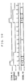
- FIG. 2 is a time chart which explains the operation of the synchronous processor circuit according to the first embodiment of the present invention.
- t1 to t19 indicate time at a regular interval.
- time t1 to time t19 indicate timings for a horizontal synchronizing signal to rise.
- the horizontal synchronizing signal is a pulse signal which rises every time at times t1 to t19.
- the vertical synchronizing signal is a pulse signal which rises at times t4 and t13 and falls at times t8 and t16.
- the composite signal 5 externally provided to a display is a synchronizing signal onto which the vertical synchronizing signal and the horizontal synchronizing signal are superimposed.
- the LPF 1 is capable of reproducing the vertical synchronization separating signal 6 with any horizontal synchronizing frequency component subtracted from the composite signal 5.
- the vertical synchronization separating signal 6 then is provided to the 1/2 frequency divider circuit 4 to be divided into 1/2, and is outputted as the vertical phase detection signal 9.
- the composite signal 5 is also provided to each of the first to sixth phase delay circuits 201 to 206 in the phase delay part 2. Those inputted composite signals 5 each generate a pulse corresponding to a period of the horizontal synchronizing signal. By using the pulses corresponding to the period of the horizontal synchronizing signal, the first to sixth phase delay circuits 201 to 206 output the horizontal synchronizing signals 19 to 24 each varied in phase with a predetermined interval, respectively.
- the horizontal synchronizing signals 19 to 24 phase-delayed as such, the vertical synchronization separating signal 6, and the vertical phase detection signal 9 are all provided to the vertical synchronizing signal reproduction circuit 3.
- the vertical synchronizing signal reproduction circuit 3 outputs the vertical synchronizing signal 8 having the phase relationship with the horizontal synchronizing signal determined.
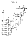
- FIG. 3 is a diagram showing an exemplary detailed structure of the vertical synchronizing signal reproduction circuit 3 of the first embodiment.
- the vertical synchronizing signal reproduction circuit 3 has almost the same structure as the vertical synchronizing signal reproduction circuit 3 in FIG. 16. Accordingly, also for the vertical synchronizing signal reproduction circuit 3 in FIG. 3, the flip-flop 10 plays a role as latch means for latching a vertical synchronization separating signal, and outputting a synchronizing signal having the phase relationship with a horizontal synchronizing signal determined.
- the multiplexer 18 plays a role as signal selection means for selecting, for output, a signal for latching the vertical synchronization separating signal from among a plurality of phase-delayed signals.
- the flip-flops 10 to 13, the NAND gates 15 and 16, and the set-reset flip-flop 17 play a role as signal selection control means for outputting a signal to control the multiplexer 18 which phase-delayed signal is selected therein.
- the vertical synchronizing signal reproduction circuit 3 in FIG. 3 is different from the one in FIG. 16 in that the flip-flops 10 to 13 are not provided with the vertical synchronization separating signal 6 but the vertical phase detection signal 9.
- the composite signal 5 onto which the horizontal synchronizing signal and the vertical synchronizing signal are superimposed is provided to the LPF 1.
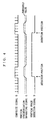
- the LPF 1 outputs the vertical synchronization separating signal 6 as shown in FIG. 4 through separation.
- This vertical synchronization separating signal 6 is provided to the 1/2 frequency divider circuit 4.
- the 1/2 frequency divider circuit 4 outputs the vertical phase detection signal 9 whose level shows change only with either one of the timings which coincide with the threshold value between the high level and the low level of the vertical synchronization separating signal 6 as shown in FIG. 4.
- the vertical phase detection signal 9 is provided to the flip-flops 10 to 13 arranged in the vertical synchronizing signal reproduction circuit 3 in FIG. 3. As shown in FIG. 18, as above described, the timings which coincide with the threshold value between the high level and the low level of the vertical synchronization separating signal 6 may differ between at the front part and the rear part thereof. With the above-described structure, however, the vertical phase detection signal 9 only shows change in level with either timing which coincides with the front part or the rear part of the vertical synchronization separating signal 6. Accordingly, as shown in FIG. 2, the output signal 27 from the multiplexer 18 is fixed to either the phase-delayed horizontal synchronizing signal 20 or 23, thereby becoming always constant.
- either the set incoming signal or reset incoming signal to the flip-flop 17 in FIG. 3 may be put invalid.
- the output signal 27 from the multiplexer 18 is surely fixable to the phase-delayed horizontal synchronizing signal 20 depending on the waveform or the threshold value of the vertical synchronization separating signal 6. Therefore, setting the set incoming signal or the reset incoming signal to the flip-flop 17 in FIG. 17 invalid is not enough to output the vertical synchronizing signal 8 whose phase can be determined with respect to the horizontal synchronizing signal.
- the phase of the vertical synchronizing signal can be determined by the horizontal synchronizing signals, whereby the stabilized vertical synchronizing signal can be supplied to each circuit arranged in the display.
- the 1/2 frequency divider circuit is included in the structure to generate the vertical phase detection signal which varies in level with either one of the timings which coincide with the threshold value between the high level and the low level of the vertical synchronization separating signal 6.
- a 1/n (where n is multiple of 2) frequency divider Circuit such as 1/4 frequency divider circuit leads to similar effects. Therefore, the frequency divider circuit in this embodiment is not limited to the 1/2 frequency divider circuit. Note herein that, if n is set too large, it becomes difficult to respond to any minute change in phase of the composite signal 5. Accordingly, needless to say, n has its own limitation in value.
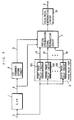
- FIG. 5 is a block diagram showing the structure of a synchronous processor circuit according to a second embodiment of the present invention.
- the synchronous processor circuit in FIG. 5 is structurally almost the same as the above-described synchronous processor circuit in FIG. 1. Note herein that, only difference between the synchronous processor circuit in FIG. 5 and the one in FIG. 1 is that a pulse width reproduction circuit 28 which receives the output signal from the vertical synchronizing reproduction circuit 3 is additionally provided. Therefore, any identical constituent is under the same reference numeral, and is not described again.
- the pulse width reproduction circuit 28 newly provided in this embodiment is described.
- the vertical synchronizing signal reproduction circuit 3 uses the vertical phase detection signal 9 to obtain the vertical synchronizing signal 8 with reference only to one timing coinciding with the threshold value between the high level and the low level of the vertical synchronization separating signal 6.
- the timing referred to for obtaining the vertical synchronizing signal 8 is the one coinciding with the threshold value at the front part of the vertical synchronization separating signal 6.
- FIG. 6 is a timing chart showing a case where such latch miss is occurred.
- latching can be assuredly carried out at the front part of the vertical synchronization separating signal 6 but is not assured for the rear part thereof. Such latch miss may degrade the display's synchronization stability.
- the synchronous processor circuit of this embodiment is so structured that the output from the vertical synchronizing signal reproduction circuit 3 goes to the pulse width reproduction circuit 28.
- This pulse width reproduction circuit 28 is structured by such counter circuit as will be later described. With this structure, as long as the reference timing is stabilized, regardless of the timing stability on the other side, the pulse width reproduction circuit 28 can output the stabilized vertical synchronizing signal 8 by taking place counting operation according to the set pulse width.
- the pulse width reproduction circuit 28 is structurally described in detail with two examples next below.
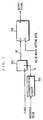
- the pulse width reproduction circuit 28 is structured as shown in FIG. 7.
- the pulse width reproduction circuit 28 includes a differentiating circuit 501 for receiving a reference pulse; a first counter 502 for receiving an output signal 51 from the differentiating circuit 501; and a comparator 503 for receiving an output signal 52 from the first counter 502 and pulse width setting data.
- the first counter 502 resets its output signal to 0 when the signal 51 provided to a reset terminal, which is denoted by R in the drawing, is in the high level, and then outputs a value obtained by incrementing from 0 on the basis of an incoming clock.
- the comparator 503 compares in value between a value A provided by the first counter 502 and the pulse width setting data B. After the comparison, if A is smaller than B, the comparator 503 outputs a signal high in level. On the other hand, if A is B or larger, the comparator 503 outputs a signal low in level.
- FIG. 8 shows a timing chart which explains the operation of such pulse width reproduction circuit 28.
- the pulse width data is fixed to 2.
- the differentiating circuit 501 outputs the signal 51 obtained by differentiating the inputted signal.
- the first counter 502 resets its counter value to 0, and then outputs the counter value obtained by incrementing from 0 in sync with an incoming clock.
- the comparator 503 monitors the value provided by the first counter 502, and keeps outputting a signal high in level until the value reaches 2 which is the pulse width setting data.
- the comparator 503 outputs a signal low in level.
- the comparator 503 keeps outputting the signal low in level.
- the pulse width reproduction circuit 28 is structured as shown in FIG. 9.
- the pulse width reproduction circuit 28 includes the differentiating circuit 501 for receiving the reference pulse; the first counter 502 for receiving an output signal 61 from the differentiating circuit 501; a second counter 504 for receiving the output signal 61 from the differentiating circuit 501 and the reference pulse; an operation circuit 505 for receiving an output signal from the second counter 504 and outputting the pulse width setting data; and the comparator 503 for receiving an output signal 62 from the first counter 502 and the pulse width setting data.
- the pulse width reproduction circuit 28 in FIG. 9 is, compared with the one in FIG. 7, additionally provided with the second counter 504 and the operation circuit 505 to generate the pulse width setting data. Since the differentiating circuit 501, the first counter 502, and the comparator 503 in FIG. 9 are identical to those in FIG. 7, the same reference numerals are provided, and the structure and the operation thereof are not described again.
- the second counter 504 if the signal 61 provided to the reset terminal, which is denoted by R in the drawing, is high in level, the second counter 504 resets its output signal to 0.
- the second counter 504 outputs a counter value counted up from 0 on the basis of the incoming clock when the reference pulse provided to its enable terminal denoted by E in the drawing is high in level. If the reference pulse is low in level, the second counter 504 outputs the current counter value as it is without counting up.
- FIG. 10 shows a timing chart which explains the operation of such second counter 504.
- the differentiating circuit 501 outputs the signal 61 obtained by differentiating the inputted reference pulse.
- the second counter 502 resets its counter value to 0.
- the second counter 502 outputs an signal 63 indicating the counter value incremented from 0 in sync with the incoming clock.
- the second counter 502 outputs the signal 63 without changing its current counter value (2 in FIG. 10).
- the operation circuit 505 performs operation with respect to the maximum value or most-frequent value of the counter value inputted from the second counter 504, and outputs a value obtained by the operation as the pulse width setting data.
- the maximum value of the counter value is 2 as is the most-frequent value. Accordingly, the operation circuit 505 sets the pulse width setting data to 2 for output.
- the comparator 503 operates similarly to the case in FIG. 7. By repeating such operation, the pulse width reproduction circuit 28 can output the stabilized signal according to the pulse width calculated based on the reference pulse.
- the pulse width reproduction circuit 28 may take any structure as long as the pulse width to be outputted is changeable by arbitrarily setting the pulse width setting data, and thus above structure is not restrictive.
- the clock used in this pulse width reproduction circuit 28 is the horizontal synchronizing signal (or composite signal), it is not restrictive and the clock may be the one which is generated from the horizontal synchronizing signal in a PLL circuit.
- the vertical synchronizing signal to be outputted therefrom can be more stabilized than the one from the synchronous processor circuit of the first embodiment.
- FIG. 11 is a block diagram showing the structure of a synchronous processor circuit according to a third embodiment of the present invention.
- the synchronous processor circuit in FIG. 11 is structurally almost the same as the above-described synchronous processor circuit in FIG. 1.
- the synchronous processor circuit in FIG. 11 is not provided with the 1/2 frequency divider circuit but is additionally provided with a flip-flop 29 for receiving the output signal from the vertical synchronizing signal reproduction circuit 3 and the phase-delayed horizontal synchronizing signal 20.
- This is the only difference between the synchronous processor circuit in FIG. 11 and the above-described one in FIG. 1.
- any identical constituent is under the same reference numeral, and is not described again.
- the flip-flop 29 newly provided in this embodiment is described.
- a signal 30 provided by the vertical synchronizing signal reproduction circuit 3 may not have a pulse width of the integral multiple of the frequency of the horizontal synchronizing signal as is described next below. Therefore, the synchronous processor circuit of this embodiment is additionally provided with the flip-flop 29, and is so structured that the signal 30 provided by the vertical synchronizing signal reproduction circuit 3 goes to a data terminal of the flip-flop 29. Further, the synchronous processor circuit is so structured that the phase-delayed horizontal synchronizing signal 20 provided to either of multiplexer 18 arranged in the vertical synchronizing signal reproduction circuit 3 goes to a clock terminal of the flip-flop 29.
- the vertical synchronizing signal 8 can be a signal whose pulse width is the integral multiple of that of the frequency of the horizontal synchronizing signal.
- FIG. 12 is a timing chart showing the case that the pulse width of the signal 30 provided by the vertical synchronizing signal reproduction circuit 3 does not become the integral multiple of that of the frequency of the horizontal synchronizing signal.
- the pulse width of the output signal from the flip-flop 29, i.e., the vertical synchronizing signal 8 becomes the integral multiple of that of the frequency of the horizontal synchronizing signal.
- the signal 30 provided by the vertical synchronizing signal reproduction circuit 3 does not become constant in horizontal synchronization frequency as described by referring to FIG. 15.
- the phase-delayed horizontal synchronizing signals 20 and 23 presumably show a phase shift of 0.5H therebetween. If so, the signal 30 outputted from the vertical synchronizing signal reproduction circuit 3 has the pulse width of 3.5H.
- the flip-flop 29 has already received the phase-delayed horizontal synchronizing signal 20 in the clock terminal. Accordingly, the vertical synchronizing signal 8 is outputted from the flip-flop 29 with the same timing as the phase-delayed horizontal synchronizing signal 20.
- the pulse width of the vertical synchronizing signal 8 outputted from the flip-flop 29 becomes the integral multiple of the pulse width of the phase-delayed horizontal synchronizing signal 20. In FIG. 12, the pulse width of the vertical synchronizing signal 8 is 4H.
- the clock for the flip-flop 29 where the pulse width reproduction is carried out is the phase-delayed horizontal synchronizing signal 20.
- the clock for the flip-flop 29 where pulse width reproduction is carried out may be a signal whose frequency is equal to that of the horizontal synchronizing signal, and is not restrictive to the phase-delayed horizontal synchronizing signal 20.
- the vertical synchronizing signal outputted therefrom can have the pulse width of the integral multiple of that of the frequency of the horizontal synchronizing signal with a simplified circuit, thereby rendering the synchronous processor circuit in the display simplified.
- FIG. 13 is a block diagram showing the structure of a synchronous processor circuit according to a fourth embodiment of the present invention.
- the synchronous processor circuit in FIG. 13 is structurally almost the same as the above-described synchronous processor circuit in FIG. 11.
- the only difference between the synchronous processor circuit in FIG. 13 and the one in FIG. 11 is that a pulse width reproduction circuit 32 for receiving the output signal from the flip-flop 29 is additionally provided. Therefore, any identical constituent is under the same reference numeral, and is not described again.
- the pulse width reproduction circuit 32 is provided to the synchronous processor circuit of this embodiment.
- the display is applicable to interlace, and an interlace signal is provided to the synchronous processor circuit.
- the clock provided to the flip-flop 29 is in a 1/2 period, that is, a pulse signal of 0.5H. Accordingly, the pulse width of the vertical synchronizing signal provided by the flip-flop 29 does not become the integral multiple of that of the frequency of the horizontal synchronizing signal.
- the synchronous processor circuit of this embodiment is so structured that the output from the flip-flop 29 goes to the pulse width reproduction circuit 12.
- the pulse width reproduction circuit 32 can set the pulse width to be outputted to an even multiple of the clock to be provided to the flip-flop 29. In such manner, it becomes possible to always set the pulse width of the vertical synchronizing signal to be the integral multiple of that of the frequency of the horizontal synchronizing signal while retaining the phase relationship between the horizontal synchronizing signals and the vertical synchronizing signal.
- the pulse width reproduction circuit 28 is already described in detail by referring to FIGS. 7 and 9. As already described, as long as the pulse width to be outputted is changeable by arbitrarily setting the pulse width setting data, the pulse width reproduction circuit 28 may take any structure.
- the vertical synchronizing signal can have the pulse width of the integral multiple of the frequency of the horizontal synchronizing signal with a simplified circuit. Therefore, it becomes possible to simplify the synchronous processor circuit in the display.
- those above-described synchronous processor circuits of the first to fourth embodiments are arranged in a display, and so structured as to reproduce a synchronizing signal from a composite signal provided by a video signal source for the display's synchronization stability.
- Such structure is made for clarity of description, and thus the synchronous processor circuit is not restricted to the case that the composite signal is provided from the video signal source.
- the synchronous processor circuit may be used for a case where a polarized synchronizing signal is provided in combination with an amplifier where voltage is pumped up.
- a display's synchronization stability can be improved by determining the phase relationship between a vertical synchronizing signal and horizontal synchronizing signals, and a synchronous processor circuit arranged in the display can be simplified by setting a pulse width of the vertical synchronizing signal to be the integral multiple of that of the frequency of the horizontal synchronizing signal.
Landscapes
- Engineering & Computer Science (AREA)
- Multimedia (AREA)
- Signal Processing (AREA)
- Synchronizing For Television (AREA)
Abstract
With the present invention, a synchronous processor circuit
can be implemented with a simplified circuit by improving a
display's synchronization stability, and by setting a pulse width
of a vertical synchronizing signal to be integral multiple of that
of the frequency of the horizontal synchronizing signal.
In a synchronous processor circuit in FIG. 1, an LPF 1
receives an externally provided composite signal 5, and a vertical
synchronization separating signal 6 is separated therefrom; a 1/2
frequency divider circuit 4 outputs a vertical phase detection
signal 9 obtained by dividing the frequency synchronization
separating signal 6 into 1/2; a phase delay part 2 receives the
composite signal 5 and outputs a plurality of horizontal
synchronizing signals 19 to 24 each differently delayed in phase;
and a vertical synchronizing signal reproduction circuit 3 uses
the vertical synchronization separating signal 6 and the
plurality of phase-delayed horizontal synchronizing signals 19
to 24 to output a vertical synchronizing signal 8 having the phase
relationship determined with respect to the horizontal
synchronizing signal.
Description
The present invention relates to synchronous processor
circuits in a color receiver and, more specifically, to a
synchronous processor circuit for reproducing a synchronizing
signal externally provided by a video signal source to a color
receiver, and supplying the synchronizing signal to each circuit
block in the color receiver.
FIG. 14 is a block diagram showing the structure of a
conventional synchronous processor circuit. In FIG. 14, the
synchronous processor circuit includes an LPF 1 to which a
composite signal 5 is externally provided, and a vertical
synchronization separating signal 6 is separated therefrom and
outputted; a phase delay part 2 for receiving the composite signal
5 and outputting a plurality of horizontal synchronizing signals
19 to 24 each differently delayed in phase; and a vertical
synchronizing signal reproduction circuit 3 for receiving the
plurality of horizontal synchronizing signals 19 to 24 each
differently delayed in phase and the vertical synchronization
separating signal 6 and outputting a vertical synchronizing
signal 8. The phase delay part 2 includes first to sixth phase
delay circuits 201 to 206. The LPF is a low pass filter. The
operation of this synchronous processor circuit is described next
below.
FIG. 15 is a time chart which explains the operation of the
conventional synchronous processor circuit. In the upper part
of the drawing, t1 to t13 indicate time at a regular interval.
To be specific, time t1 to time t13 indicate timing for a horizontal
synchronizing signal to rise. As shown in FIG. 15, the composite
signal 5 externally provided to a display is a synchronizing
signal onto which a vertical synchronizing signal and a horizontal
synchronizing signal are superimposed.
In FIG. 15, the horizontal synchronizing signal is a pulse
signal which rises every time at times t1 to time t13. The
vertical synchronizing signal is a pulse signal which rises at
time t4 and falls at time t8. Once inputted into the LPF 1, such
composite signal 5 is cut off with any horizontal synchronizing
frequency component which is high in frequency. Therefore, the
LPF 1 is capable of reproducing the vertical synchronization
separating signal 6 with any horizontal synchronizing frequency
component subtracted from the composite signal 5.
The composite signal 5 is also provided to each of the first
to sixth phase delay circuits 201 to 206 in the phase delay part
2. Those inputted composite signals 5 each generate a pulse
corresponding to a period of the horizontal synchronizing signal.
By using the pulses corresponding to the period of the horizontal
synchronizing signal, the first to sixth phase delay circuits 201
to 206 output horizontal synchronizing signals 19 to 24 varied
in phase with a predetermined interval in the corresponding phase
delay circuit, respectively. The horizontal synchronizing
signals 19 to 24 phase-delayed as such and the vertical
synchronization separating signal 6 are provided to the vertical
synchronizing signal reproduction circuit 3. The vertical
synchronizing signal reproduction circuit 3 outputs the vertical
synchronizing signal 8 having the phase relationship with the
horizontal synchronizing signal determined.
Next, the vertical synchronizing signal reproduction
circuit 3 is described for its structure and operation in detail.
FIG. 16 is a diagram showing an exemplary detailed structure of
the vertical synchronizing signal reproduction circuit 3. In FIG.
16, the vertical synchronizing signal reproduction circuit 3
includes flip-flops 10 to 13, each of which receives the
phase-delayed horizontal synchronizing signal 19, 21, 22, or 24
and the vertical synchronization separating signal 6; a NAND gate
15 which receives signals from the flip- flops 10 and 11; a NAND
gate 16 which receives signals from the flip- flops 12 and 13; a
set-reset flip-flop 17 in which a signal from the NAND gate 15
goes to the set and a signal from the NAND gate 16 to the reset;
a multiplexer 18 which receives a signal from the set-reset
flip-flop 17 as a control signal and the phase-delayed horizontal
synchronizing signals 20 and 23, and outputs a signal 27 which
is either one of the horizontal synchronizing signals; and a
flip-flop 10 which receives the vertical synchronization
separating signal 6 and the output signal 27 from the multiplexer
18, and outputs the vertical synchronizing signal 8.
In FIG. 16, the flip-flop 10 plays a role as latch means
for latching a vertical synchronization separating signal, and
outputting a synchronizing signal having the phase relationship
with the horizontal synchronizing signal determined. The
multiplexer 18 plays a role as signal selection means for
selecting, for output, a signal for latching the vertical
synchronization separating signal from among a plurality of
phase-delayed signals. The flip-flops 10 to 13, the NAND gates
15 and 16, and the set-reset flip-flop 17 play a role as signal
selection control means for outputting a signal to control the
multiplexer 18 which phase-delayed signal is selected therein.
The operation of such structured vertical synchronizing signal
reproduction circuit 3 is described next below by referring to
FIGS. 16 and 17.
FIG. 17 is a time chart showing the operation of the vertical
synchronizing signal reproduction circuit 3 from time t4 to time
t5 in FIG. 15. In FIG. 17, a timing (denoted by time tA in the
drawing) which coincides with a threshold value between a high
level and a low level of the vertical synchronization separating
signal 6 is observed between timings for the phase- delayed
synchronizing signals 19 and 21 to rise. In such case, as shown
in FIG. 17, the output signal from the NAND gate 15 changes in
level from high to low with the timing when the phase-delayed
horizontal synchronizing signal 21 rises. The signal is a set
incoming signal 25 which is inputted into the set terminal of the
set-reset flip-flop 17.
Further, in FIG. 17, the timing which coincides with the
threshold value between the high level and the low level of the
vertical synchronization separating signal 6 is not observed
between timings for the phase-delayed horizontal synchronizing
signals 22 and 24 to rise. Therefore, as shown in FIG. 17, an
output signal 26 from the NAND gate 16 remains in the high level.
The signal is a reset incoming signal 26 which is inputted into
the reset terminal of the set-reset flip-flop 17.
Once such set incoming signal 25 and reset incoming signal
26 are provided to the set-reset flip-flop 17, as shown in FIG.
17, an output signal 33 from the set-reset flip-flop 17 is fixed
in the low level. The output signal 33 from the set-reset
flip-flop 17 is provided to a control terminal of the multiplexer
18.
When receiving a signal high in level in the control
terminal, the multiplexer 18 selects the phase-delayed
horizontal synchronizing signal 20 for output. When a signal low
in level is inputted thereto, the multiplexer 18 selects the
phase-delayed horizontal synchronizing signal 23 for output.
Accordingly, the multiplexer 18 having the signal low in level
provided to its control terminal selects and outputs the
phase-delayed horizontal synchronizing signal 23.
The phase-delayed horizontal synchronizing signal 23 can
assuredly be latched with the vertical synchronization separating
signal 6 with the timing which coincides with the threshold value
between the high level and low level thereof. This is because,
as described in the foregoing, the timing which coincides with
the threshold value between the high level and the low level of
the vertical synchronization separating signal 6 is observed
between the timings for the phase-delayed horizontal
synchronizing signals 19 and 21 to rise. Therefore, it is not
certain whether the phase-delayed horizontal synchronizing
signal 20 between the phase-delayed horizontal synchronizing
signals 19 and 21 is capable for latching. Accordingly, the
flip-flop 14 can assuredly latch the vertical synchronization
separating signal 6 with the help of the phase-delayed horizontal
synchronizing signal 23.
In the foregoing, by referring to FIG. 17, it has been
exemplarily described the case where the timing which coincides
with the threshold value between the high level and the low level
of the vertical synchronization separating signal 6 is observed
between the phase-delayed horizontal synchronizing signals 19 arid
21. Herein, the timing which coincides with the threshold value
between the high level and the low level of the vertical
synchronization separating signal 6 may be observed between the
timings for the phase-delayed horizontal synchronizing signals
22 and 24 to rise. In such case, the multiplexer 18 selects, for
output, not the phase-delayed horizontal synchronizing signal 23
but the phase-delayed horizontal synchronizing signal 20.
Accordingly, similar to the above-described case, the flip-flop
14 can assuredly latch the vertical synchronization separating
signal 6.
In such manner, by receiving the phase-delayed horizontal
synchronizing signals 19 to 24 from the phase delay part 2 as
signals for detecting the timing which coincides with the
threshold value between the high level and the low level of the
vertical synchronization separating signal 6, the vertical
synchronizing signal reproduction circuit 3 can determine the
phase relationship between the vertical synchronizing signal and
the horizontal synchronization signals. As such, the vertical
synchronizing signal reproduction circuit 3 can assuredly latch
the vertical synchronization separating signal 6, and thus can
supply, to each digital signal processor circuit arranged in the
display, the vertical synchronizing signal 8 which has been
accurately reproduced.
According to the conventional synchronous processor
circuit structured as such, however, a stabilized vertical
synchronizing signal cannot be assuredly obtained if, as shown
in FIG. 15, the timings which coincide with the threshold value
between the high level and the low level of the vertical
synchronization separating signal 6 separated and reproduced by
the LPF 1 approximately coincide with both pulse timings of the
phase-delayed horizontal synchronizing signals 20 and 23. This
is because the phase relationship between the vertical
synchronization separating signal 6 and the horizontal
synchronizing signal is not determined.
FIGS. 18 are diagrams schematically showing a
partially-enlarged waveform of the vertical synchronization
separating signal 6. A dotted line laterally drawn in the
drawings indicates the threshold value between the high level and
the low level of the vertical synchronization separating signal
6. To be specific, the threshold value is used by the flip-flops
10 to 14 which receive the vertical synchronization separating
signal 6 to distinguish the level thereof between high and low.
FIG. 18(a) is the diagram schematically showing the
waveform at a front part of the vertical synchronization
separating signal 6 in the range between time t4 and time t5 in
FIG. 11. In the drawing, tA indicates a time when the vertical
synchronization separating signal 6 reaches the threshold value
as in FIG. 17. In the drawing, Ts indicates a period between time
t4 and time tA. FIG. 18(b) is the diagram schematically showing
the waveform at a rear part of the vertical synchronization
separating signal 6 in the range between time t8 and time t9 in
FIG. 11. In the drawing, tB indicates a time when the vertical
synchronization separating signal 6 reaches the threshold value.
In the drawing, Te indicates a period between time t8 and time
tB.
As shown in FIG. 18, the waveform of the vertical
synchronization separating signal 6 often differs in shape
between the front part and the rear part, and the timings tA and
tB which coincide with the threshold value between the high level
and the low level of the vertical synchronization separating
signal 6 often differ between the front part and the rear part
thereof. Therefore, at the rear part of the vertical
synchronization separating signal 6, unlike the above-described
case in FIG. 17, the timing which coincides with the threshold
value between the high level and the low level of the vertical
synchronization separating signal 6 may be observed between the
timings for the phase-delayed horizontal synchronizing signals
22 and 24 to rise. If this is the case, the multiplexer 18 may
select, for output, the phase-delayed horizontal synchronizing
signal 20, or the phase-delayed horizontal synchronizing signal
23. Consequently, the output signal 27 from the multiplexer 18
fails to be constant in horizontal synchronizing frequency as
shown in FIG. 15. As such, according to the conventional
structure, the phase relationship between the vertical
synchronization separating signal 6 and the horizontal
synchronizing signal is not determined. Therefore, the vertical
synchronization signal provided therefrom cannot be stabilized
enough.
Further, in such case as shown in FIG. 15, as to the vertical
synchronizing signal provided by the vertical synchronizing
signal reproduction circuit 3, a pulse width thereof does not
become integral multiple of that of the frequency of the
horizontal synchronizing signal. Consequently, the synchronous
processor circuit in the display becomes complicated in structure,
thereby rendering the cost increased.
Especially, such phenomenon often occurs in a multiscan
monitor, which receives incoming signals varied in scanning
frequency from a video signal source. Generally, the LPF 1 is
fixed in cutoff frequency. Therefore, the cutoff frequency of
the LPF 1 may be too heavy (too low) for the vertical synchronizing
signal component superimposed on the composite signal 5 depending
on its pulse width. If this is the case, the vertical
synchronization separating signal 6 provided by the LPF 1 may get
very blunt. As exemplarily shown in FIG. 18, the vertical
synchronization separating signal 6 provided by the LPF 1 shows
a gradual change from time t4 to time t5, or from time t4 and time
t5. As a result, as described in the foregoing, the timings which
coincide with the threshold value between the high level and the
low level of the vertical synchronization separating signal 6
approximately coincide with both pulse timings of the above-described
phase-delayed horizontal synchronizing signals 20 and
23, thereby causing such problem as above-described.
Therefore, an object of the present invention is to provide
a synchronous processor circuit capable of improving a display's
synchronization stability by determining a phase relationship
between a vertical synchronizing signal and horizontal
synchronizing signals, and circuitry structure of which can be
simplified by setting a pulse width of the vertical synchronizing
signal to be the integral multiple of the frequency of the
horizontal synchronizing signal.
A first aspect of the present invention is directed to a
synchronous processor circuit arranged in a display for
reproducing a synchronizing signal from a composite signal
provided by a video signal source for stabilizing synchronization
in the display, the circuit comprising:
As described above, in the first aspect of the present
invention, it becomes possible to determine the phase
relationship between the vertical synchronizing signal and the
horizontal synchronizing signal. Accordingly, the stabilized
vertical synchronizing signal can be supplied to each circuit
arranged in the display.
According to a second aspect of the present invention, in
the first aspect of the present invention,
the frequency divider circuit outputs the vertical phase detection signal obtained by dividing the cycle of the vertical synchronizing signal into 1/2.
the frequency divider circuit outputs the vertical phase detection signal obtained by dividing the cycle of the vertical synchronizing signal into 1/2.
As described above, in the second aspect of the present
invention, it becomes possible to swiftly respond to any minute
change in phase of the incoming composite signal by having the
1/2 frequency divider circuit provided. Accordingly, the
stabilized vertical synchronizing signal can be supplied to each
circuit arranged in the display.
According to a third aspect of the present invention, in
the first aspect of the present invention,
the vertical synchronizing signal reproduction circuit comprises:
the vertical synchronizing signal reproduction circuit comprises:
As described above, according to the third aspect of the
present invention, the phase relationship between the vertical
synchronizing signal and the horizontal synchronizing signal can
be determined with the help of a plurality of phase-delayed
signals inputted as signals for detecting a timing which coincides
with the threshold value between the high level and the low level
of the vertical synchronization separating signal.
According to a fourth aspect of the present invention, in
the first aspect of the present invention,
the synchronous processor circuit further comprises a pulse width reproduction circuit for receiving the signal from the vertical synchronizing signal reproduction circuit, and reproducing the synchronizing signal having a predetermined pulse width.
the synchronous processor circuit further comprises a pulse width reproduction circuit for receiving the signal from the vertical synchronizing signal reproduction circuit, and reproducing the synchronizing signal having a predetermined pulse width.
As described above, according to the fourth aspect of the
present invention, as long as the reference timing is stabilized,
regardless of the other timing's stability, the stabilized
vertical synchronizing signal can be outputted with the counting
operation carried out according to the set pulse width.
According to a fifth aspect of the present invention, in
the fourth aspect of the present invention,
the pulse width reproduction circuit comprises:
the pulse width reproduction circuit comprises:
As described above, in the fifth aspect of the present
invention, the pulse width reproduction circuit can output the
stabilized signal according to the pulse width which is previously
set or calculated by operation.
A sixth aspect of the present invention is directed to a
synchronous processor circuit arranged in a display for
reproducing a synchronizing signal from a composite signal
provided by a video signal source for stabilizing synchronization
in the display, the circuit comprising:
As described above, in the sixth aspect of the present
invention, it is possible to obtain the vertical synchronizing
signal having the pulse width of the integral multiple of that
of the frequency of the horizontal synchronizing signal with a
structurally simplified circuit. Accordingly, the synchronous
processor circuit in the display can be simplified in structure.
According to a seventh aspect of the present invention, in
the sixth aspect of the present invention,
the vertical synchronizing signal reproduction circuit comprises:
the vertical synchronizing signal reproduction circuit comprises:
As described above, in the seventh aspect of the present
invention, the phase relationship between the vertical
synchronizing signal and the horizontal synchronizing signal can
be determined with the help of a plurality of phase-delayed
signals inputted as signals for detecting a timing which coincides
with the threshold value between the high level and the low level
of the vertical synchronization separating signal.
According to an eighth aspect of the present invention, in
the sixth aspect of the present invention,
the synchronous processor circuit further comprises a pulse width reproduction circuit for receiving the signal from the flip-flop, and reproducing the synchronizing signal having a predetermined pulse width.
the synchronous processor circuit further comprises a pulse width reproduction circuit for receiving the signal from the flip-flop, and reproducing the synchronizing signal having a predetermined pulse width.
As described above, in the eighth aspect of the present
invention, as long as the reference timing is stabilized,
regardless of the other timing's stability, the stabilized
vertical synchronizing signal can be outputted with the counting
operation carried out according to the set pulse width. Therefore,
with a structurally simplified circuit, even with respect to the
interlace signal, the vertical synchronizing signal can have the
pulse width of the integral multiple of the frequency of the
horizontal synchronizing signal. Therefore, it becomes possible
to simplify the synchronous processor circuit in the display.
According to a ninth aspect of the present invention, in
the eighth aspect of the present invention,
the pulse width reproduction circuit comprises:
the pulse width reproduction circuit comprises:
As described above, in the ninth aspect of the present
invention, the pulse width reproduction circuit can output the
stabilized signal according to the pulse width which is previously
set or calculated by operation.
FIG. 1 is a block diagram showing the structure of a
synchronous processor circuit according to a first embodiment of
the present invention. In FIG. 1, the synchronous processor
circuit includes the LPF 1 to which the composite signal 5 is
externally provided, and the vertical synchronization separating
signal 6 is separated therefrom for output; a 1/2 frequency
divider circuit 4 for receiving the vertical synchronization
separating signal 6 and subjecting the signal to 1/2 frequency
division to output a vertical phase detection signal 9; the phase
delay part 2 for receiving the composite signal 5 and outputting
the plurality of horizontal synchronizing signals 19 to 24 each
differently delayed in phase; and the vertical synchronizing
signal reproduction circuit 3 for receiving the plurality of
phase-delayed horizontal synchronizing signals 19 to 24, the
vertical synchronization separating signal 6, and the vertical
phase detection signal 9, and outputting the vertical
synchronizing signal 8. The phase delay part 2 includes the first
to sixth phase delay circuits 201 to 206. The operation of the
synchronous processor circuit is described next below.
FIG. 2 is a time chart which explains the operation of the
synchronous processor circuit according to the first embodiment
of the present invention. In the upper part of the drawing, t1
to t19 indicate time at a regular interval. To be specific, time
t1 to time t19 indicate timings for a horizontal synchronizing
signal to rise.
In FIG. 2, similarly in FIG. 15, the horizontal
synchronizing signal is a pulse signal which rises every time at
times t1 to t19. The vertical synchronizing signal is a pulse
signal which rises at times t4 and t13 and falls at times t8 and
t16.
As shown in FIG. 2, the composite signal 5 externally
provided to a display is a synchronizing signal onto which the
vertical synchronizing signal and the horizontal synchronizing
signal are superimposed. Once provided to the LPF 1, such
composite signal 5 is cut off with any horizontal frequency
component high in frequency. Therefore, the LPF 1 is capable of
reproducing the vertical synchronization separating signal 6 with
any horizontal synchronizing frequency component subtracted from
the composite signal 5. The vertical synchronization separating
signal 6 then is provided to the 1/2 frequency divider circuit
4 to be divided into 1/2, and is outputted as the vertical phase
detection signal 9.
The composite signal 5 is also provided to each of the first
to sixth phase delay circuits 201 to 206 in the phase delay part
2. Those inputted composite signals 5 each generate a pulse
corresponding to a period of the horizontal synchronizing signal.
By using the pulses corresponding to the period of the horizontal
synchronizing signal, the first to sixth phase delay circuits 201
to 206 output the horizontal synchronizing signals 19 to 24 each
varied in phase with a predetermined interval, respectively.
The horizontal synchronizing signals 19 to 24 phase-delayed
as such, the vertical synchronization separating signal 6, and
the vertical phase detection signal 9 are all provided to the
vertical synchronizing signal reproduction circuit 3. The
vertical synchronizing signal reproduction circuit 3 outputs the
vertical synchronizing signal 8 having the phase relationship
with the horizontal synchronizing signal determined.
Next, the vertical synchronizing signal reproduction
circuit 3 is described for its structure and operation in detail.
FIG. 3 is a diagram showing an exemplary detailed structure of
the vertical synchronizing signal reproduction circuit 3 of the
first embodiment. In FIG. 3, the vertical synchronizing signal
reproduction circuit 3 has almost the same structure as the
vertical synchronizing signal reproduction circuit 3 in FIG. 16.
Accordingly, also for the vertical synchronizing signal
reproduction circuit 3 in FIG. 3, the flip-flop 10 plays a role
as latch means for latching a vertical synchronization separating
signal, and outputting a synchronizing signal having the phase
relationship with a horizontal synchronizing signal determined.
The multiplexer 18 plays a role as signal selection means for
selecting, for output, a signal for latching the vertical
synchronization separating signal from among a plurality of
phase-delayed signals. The flip-flops 10 to 13, the NAND gates
15 and 16, and the set-reset flip-flop 17 play a role as signal
selection control means for outputting a signal to control the
multiplexer 18 which phase-delayed signal is selected therein.
Note herein that, the vertical synchronizing signal
reproduction circuit 3 in FIG. 3 is different from the one in FIG.
16 in that the flip-flops 10 to 13 are not provided with the
vertical synchronization separating signal 6 but the vertical
phase detection signal 9.
The operation of such structured vertical synchronizing
signal reproduction circuit 3 is described by referring to FIG.
4. The operation of any component in FIG. 3 identical to that
in the vertical synchronizing signal reproduction circuit 3 is
not described again.
In FIG. 4, the composite signal 5 onto which the horizontal
synchronizing signal and the vertical synchronizing signal are
superimposed is provided to the LPF 1. The LPF 1 outputs the
vertical synchronization separating signal 6 as shown in FIG. 4
through separation. This vertical synchronization separating
signal 6 is provided to the 1/2 frequency divider circuit 4. The
1/2 frequency divider circuit 4 outputs the vertical phase
detection signal 9 whose level shows change only with either one
of the timings which coincide with the threshold value between
the high level and the low level of the vertical synchronization
separating signal 6 as shown in FIG. 4.
The vertical phase detection signal 9 is provided to the
flip-flops 10 to 13 arranged in the vertical synchronizing signal
reproduction circuit 3 in FIG. 3. As shown in FIG. 18, as above
described, the timings which coincide with the threshold value
between the high level and the low level of the vertical
synchronization separating signal 6 may differ between at the
front part and the rear part thereof. With the above-described
structure, however, the vertical phase detection signal 9 only
shows change in level with either timing which coincides with the
front part or the rear part of the vertical synchronization
separating signal 6. Accordingly, as shown in FIG. 2, the output
signal 27 from the multiplexer 18 is fixed to either the
phase-delayed horizontal synchronizing signal 20 or 23, thereby
becoming always constant.
In order to achieve such structure in which the output
signal 27 from the multiplexer 18 is fixed to either the
phase-delayed horizontal synchronizing signal 20 or 23 to be
always constant, for example, either the set incoming signal or
reset incoming signal to the flip-flop 17 in FIG. 3 may be put
invalid. Although being fixed to the phase-delayed horizontal
synchronizing signal 23 in FIG. 2, the output signal 27 from the
multiplexer 18 is surely fixable to the phase-delayed horizontal
synchronizing signal 20 depending on the waveform or the threshold
value of the vertical synchronization separating signal 6.
Therefore, setting the set incoming signal or the reset incoming
signal to the flip-flop 17 in FIG. 17 invalid is not enough to
output the vertical synchronizing signal 8 whose phase can be
determined with respect to the horizontal synchronizing signal.
As is known from the above, according to the structure of
the synchronous processor circuit of this embodiment, the phase
of the vertical synchronizing signal can be determined by the
horizontal synchronizing signals, whereby the stabilized
vertical synchronizing signal can be supplied to each circuit
arranged in the display.
Herein, in this embodiment, the 1/2 frequency divider
circuit is included in the structure to generate the vertical
phase detection signal which varies in level with either one of
the timings which coincide with the threshold value between the
high level and the low level of the vertical synchronization
separating signal 6. However, instead of the 1/2 frequency
divider circuit, a 1/n (where n is multiple of 2) frequency divider
Circuit such as 1/4 frequency divider circuit leads to similar
effects. Therefore, the frequency divider circuit in this
embodiment is not limited to the 1/2 frequency divider circuit.
Note herein that, if n is set too large, it becomes difficult to
respond to any minute change in phase of the composite signal 5.
Accordingly, needless to say, n has its own limitation in value.
FIG. 5 is a block diagram showing the structure of a
synchronous processor circuit according to a second embodiment
of the present invention. The synchronous processor circuit in
FIG. 5 is structurally almost the same as the above-described
synchronous processor circuit in FIG. 1. Note herein that, only
difference between the synchronous processor circuit in FIG. 5
and the one in FIG. 1 is that a pulse width reproduction circuit
28 which receives the output signal from the vertical
synchronizing reproduction circuit 3 is additionally provided.
Therefore, any identical constituent is under the same reference
numeral, and is not described again.
Herein, the pulse width reproduction circuit 28 newly
provided in this embodiment is described. In the synchronous
processor circuit according to the first embodiment of the present
invention, the vertical synchronizing signal reproduction
circuit 3 uses the vertical phase detection signal 9 to obtain
the vertical synchronizing signal 8 with reference only to one
timing coinciding with the threshold value between the high level
and the low level of the vertical synchronization separating
signal 6. In FIG. 2, the timing referred to for obtaining the
vertical synchronizing signal 8 is the one coinciding with the
threshold value at the front part of the vertical synchronization
separating signal 6.
With such structure, if the output signal 27 from the
multiplexer 18 is used to latch not with the referred timing but
with the timing on the other side (at the rear part of the vertical
synchronizing separating signal 6 in FIG. 2) which coincides with
the threshold value between the high level and the low level, a
latch miss may be occurred. FIG. 6 is a timing chart showing a
case where such latch miss is occurred.
As shown in FIG. 6, in the synchronous processor circuit
of the first embodiment, latching can be assuredly carried out
at the front part of the vertical synchronization separating
signal 6 but is not assured for the rear part thereof. Such latch
miss may degrade the display's synchronization stability.
Therefore, the synchronous processor circuit of this
embodiment, as shown in FIG. 5, is so structured that the output
from the vertical synchronizing signal reproduction circuit 3
goes to the pulse width reproduction circuit 28. This pulse width
reproduction circuit 28 is structured by such counter circuit as
will be later described. With this structure, as long as the
reference timing is stabilized, regardless of the timing
stability on the other side, the pulse width reproduction circuit
28 can output the stabilized vertical synchronizing signal 8 by
taking place counting operation according to the set pulse width.
Such pulse width reproduction circuit 28 is structurally
described in detail with two examples next below. In a first
example, the pulse width reproduction circuit 28 is structured
as shown in FIG. 7. In FIG. 7, the pulse width reproduction
circuit 28 includes a differentiating circuit 501 for receiving
a reference pulse; a first counter 502 for receiving an output
signal 51 from the differentiating circuit 501; and a comparator
503 for receiving an output signal 52 from the first counter 502
and pulse width setting data.
The first counter 502 resets its output signal to 0 when
the signal 51 provided to a reset terminal, which is denoted by
R in the drawing, is in the high level, and then outputs a value
obtained by incrementing from 0 on the basis of an incoming clock.
The comparator 503 compares in value between a value A provided
by the first counter 502 and the pulse width setting data B. After
the comparison, if A is smaller than B, the comparator 503 outputs
a signal high in level. On the other hand, if A is B or larger,
the comparator 503 outputs a signal low in level.
FIG. 8 shows a timing chart which explains the operation
of such pulse width reproduction circuit 28. In FIG. 8, the pulse
width data is fixed to 2. Once the reference pulse is inputted,
the differentiating circuit 501 outputs the signal 51 obtained
by differentiating the inputted signal. After the signal 51 is
inputted, the first counter 502 resets its counter value to 0,
and then outputs the counter value obtained by incrementing from
0 in sync with an incoming clock. The comparator 503 monitors
the value provided by the first counter 502, and keeps outputting
a signal high in level until the value reaches 2 which is the pulse
width setting data. When the value provided by the first counter
502 reached 2, the comparator 503 outputs a signal low in level.
Thereafter, until the value provided from the first counter 502
returns to 0, the comparator 503 keeps outputting the signal low
in level. By repeating such operation, the pulse width
reproduction circuit 28 becomes capable of outputting a
stabilized signal according to the set pulse width.
In a second example, the pulse width reproduction circuit
28 is structured as shown in FIG. 9. In FIG. 9, the pulse width
reproduction circuit 28 includes the differentiating circuit 501
for receiving the reference pulse; the first counter 502 for
receiving an output signal 61 from the differentiating circuit
501; a second counter 504 for receiving the output signal 61 from
the differentiating circuit 501 and the reference pulse; an
operation circuit 505 for receiving an output signal from the
second counter 504 and outputting the pulse width setting data;
and the comparator 503 for receiving an output signal 62 from the
first counter 502 and the pulse width setting data.
The pulse width reproduction circuit 28 in FIG. 9 is,
compared with the one in FIG. 7, additionally provided with the
second counter 504 and the operation circuit 505 to generate the
pulse width setting data. Since the differentiating circuit 501,
the first counter 502, and the comparator 503 in FIG. 9 are
identical to those in FIG. 7, the same reference numerals are
provided, and the structure and the operation thereof are not
described again.
In FIG. 9, if the signal 61 provided to the reset terminal,
which is denoted by R in the drawing, is high in level, the second
counter 504 resets its output signal to 0. The second counter
504 outputs a counter value counted up from 0 on the basis of the
incoming clock when the reference pulse provided to its enable
terminal denoted by E in the drawing is high in level. If the
reference pulse is low in level, the second counter 504 outputs
the current counter value as it is without counting up.
FIG. 10 shows a timing chart which explains the operation
of such second counter 504. In FIG. 10, the differentiating
circuit 501 outputs the signal 61 obtained by differentiating the
inputted reference pulse. Once the signal 61 is provided, the
second counter 502 resets its counter value to 0. At this time,
since the reference pulse provided to the enable terminal of the
second counter 502 is high in level, the second counter 502 outputs
an signal 63 indicating the counter value incremented from 0 in
sync with the incoming clock. Thereafter, when the reference
pulse provided to the enable terminal becomes low in level, the
second counter 502 outputs the signal 63 without changing its
current counter value (2 in FIG. 10).
The operation circuit 505 performs operation with respect
to the maximum value or most-frequent value of the counter value
inputted from the second counter 504, and outputs a value obtained
by the operation as the pulse width setting data. In FIG. 10,
the maximum value of the counter value is 2 as is the most-frequent
value. Accordingly, the operation circuit 505 sets the pulse
width setting data to 2 for output. The comparator 503 operates
similarly to the case in FIG. 7. By repeating such operation,
the pulse width reproduction circuit 28 can output the stabilized
signal according to the pulse width calculated based on the
reference pulse.
Herein, the pulse width reproduction circuit 28 may take
any structure as long as the pulse width to be outputted is
changeable by arbitrarily setting the pulse width setting data,
and thus above structure is not restrictive. Although the clock
used in this pulse width reproduction circuit 28 is the horizontal
synchronizing signal (or composite signal), it is not restrictive
and the clock may be the one which is generated from the horizontal
synchronizing signal in a PLL circuit.
As is known from the above, according to the synchronous
processor circuit of the second embodiment which is additionally
provided with the pulse width reproduction circuit 28 compared
with the synchronous processor circuit of the first embodiment,
the vertical synchronizing signal to be outputted therefrom can
be more stabilized than the one from the synchronous processor
circuit of the first embodiment.
FIG. 11 is a block diagram showing the structure of a
synchronous processor circuit according to a third embodiment of
the present invention. The synchronous processor circuit in FIG.
11 is structurally almost the same as the above-described
synchronous processor circuit in FIG. 1. Note herein that, the
synchronous processor circuit in FIG. 11 is not provided with the
1/2 frequency divider circuit but is additionally provided with
a flip-flop 29 for receiving the output signal from the vertical
synchronizing signal reproduction circuit 3 and the phase-delayed
horizontal synchronizing signal 20. This is the only difference
between the synchronous processor circuit in FIG. 11 and the
above-described one in FIG. 1. Thus, any identical constituent
is under the same reference numeral, and is not described again.
Next, the flip-flop 29 newly provided in this embodiment
is described. In the synchronous processor circuit of this
embodiment, a signal 30 provided by the vertical synchronizing
signal reproduction circuit 3 may not have a pulse width of the
integral multiple of the frequency of the horizontal
synchronizing signal as is described next below. Therefore, the
synchronous processor circuit of this embodiment is additionally
provided with the flip-flop 29, and is so structured that the
signal 30 provided by the vertical synchronizing signal
reproduction circuit 3 goes to a data terminal of the flip-flop
29. Further, the synchronous processor circuit is so structured
that the phase-delayed horizontal synchronizing signal 20
provided to either of multiplexer 18 arranged in the vertical
synchronizing signal reproduction circuit 3 goes to a clock
terminal of the flip-flop 29. With such structured synchronous
processor circuit, the vertical synchronizing signal 8 can be a
signal whose pulse width is the integral multiple of that of the
frequency of the horizontal synchronizing signal.
FIG. 12 is a timing chart showing the case that the pulse
width of the signal 30 provided by the vertical synchronizing
signal reproduction circuit 3 does not become the integral
multiple of that of the frequency of the horizontal synchronizing
signal. With reference to FIG. 12, it is now described why the
pulse width of the output signal from the flip-flop 29, i.e., the
vertical synchronizing signal 8 becomes the integral multiple of
that of the frequency of the horizontal synchronizing signal.
In FIG. 12, the signal 30 provided by the vertical
synchronizing signal reproduction circuit 3 does not become
constant in horizontal synchronization frequency as described by
referring to FIG. 15. In FIG. 12, the phase-delayed horizontal
synchronizing signals 20 and 23 presumably show a phase shift of
0.5H therebetween. If so, the signal 30 outputted from the
vertical synchronizing signal reproduction circuit 3 has the
pulse width of 3.5H. Herein, the flip-flop 29 has already
received the phase-delayed horizontal synchronizing signal 20 in
the clock terminal. Accordingly, the vertical synchronizing
signal 8 is outputted from the flip-flop 29 with the same timing
as the phase-delayed horizontal synchronizing signal 20. As such,
the pulse width of the vertical synchronizing signal 8 outputted
from the flip-flop 29 becomes the integral multiple of the pulse
width of the phase-delayed horizontal synchronizing signal 20.
In FIG. 12, the pulse width of the vertical synchronizing signal
8 is 4H.
In this embodiment, the clock for the flip-flop 29 where
the pulse width reproduction is carried out is the phase-delayed
horizontal synchronizing signal 20. However, other phase-delayed
horizontal synchronizing signals 19 and 21 to 24 lead to
the similar effects. By taking this into consideration, the clock
for the flip-flop 29 where pulse width reproduction is carried
out may be a signal whose frequency is equal to that of the
horizontal synchronizing signal, and is not restrictive to the
phase-delayed horizontal synchronizing signal 20.
With such structured synchronous processor circuit
according to the third embodiment of the present invention, the
vertical synchronizing signal outputted therefrom can have the
pulse width of the integral multiple of that of the frequency of
the horizontal synchronizing signal with a simplified circuit,
thereby rendering the synchronous processor circuit in the
display simplified.
FIG. 13 is a block diagram showing the structure of a
synchronous processor circuit according to a fourth embodiment
of the present invention. The synchronous processor circuit in
FIG. 13 is structurally almost the same as the above-described
synchronous processor circuit in FIG. 11. The only difference
between the synchronous processor circuit in FIG. 13 and the one
in FIG. 11 is that a pulse width reproduction circuit 32 for
receiving the output signal from the flip-flop 29 is additionally
provided. Therefore, any identical constituent is under the same
reference numeral, and is not described again.
Next, the reason why the pulse width reproduction circuit
32 is provided to the synchronous processor circuit of this
embodiment is described. Herein, it is assumed that the display
is applicable to interlace, and an interlace signal is provided
to the synchronous processor circuit. In such case, the clock
provided to the flip-flop 29 is in a 1/2 period, that is, a pulse
signal of 0.5H. Accordingly, the pulse width of the vertical
synchronizing signal provided by the flip-flop 29 does not become
the integral multiple of that of the frequency of the horizontal
synchronizing signal.
In this respect, in order to have the display applicable
to interlace, it is conventionally known that a double-speed
horizontal synchronizing signal generation circuit in which the
frequency of the horizontal synchronizing signal is doubly
multiplied so as to stabilize the phase relationship between the
vertical synchronizing signal and the horizontal synchronizing
signals. However, even if the interlace signal is handled in such
conventional structure, the period of the clock to be provided
to the flip-flop 29 remains 1/2 of the cycle of the horizontal
synchronizing signal. Consequently, the pulse width of the
vertical synchronizing signal from the flip-flop 29 does not
become the integral multiple of the frequency of the horizontal
synchronizing signal.
Therefore, as shown in FIG. 13, the synchronous processor
circuit of this embodiment is so structured that the output from
the flip-flop 29 goes to the pulse width reproduction circuit 12.
In FIG. 13, by arbitrarily setting the pulse width setting data,
the pulse width reproduction circuit 32 can set the pulse width
to be outputted to an even multiple of the clock to be provided
to the flip-flop 29. In such manner, it becomes possible to always
set the pulse width of the vertical synchronizing signal to be
the integral multiple of that of the frequency of the horizontal
synchronizing signal while retaining the phase relationship
between the horizontal synchronizing signals and the vertical
synchronizing signal.
The structure of the pulse width reproduction circuit 28
is already described in detail by referring to FIGS. 7 and 9. As
already described, as long as the pulse width to be outputted is
changeable by arbitrarily setting the pulse width setting data,
the pulse width reproduction circuit 28 may take any structure.
With such structured synchronous processor circuit of this
embodiment, even with respect also to the interlace signal, the
vertical synchronizing signal can have the pulse width of the
integral multiple of the frequency of the horizontal
synchronizing signal with a simplified circuit. Therefore, it
becomes possible to simplify the synchronous processor circuit
in the display.
Lastly, those above-described synchronous processor
circuits of the first to fourth embodiments are arranged in a
display, and so structured as to reproduce a synchronizing signal
from a composite signal provided by a video signal source for the
display's synchronization stability. Such structure, however,
is made for clarity of description, and thus the synchronous
processor circuit is not restricted to the case that the composite
signal is provided from the video signal source. As an example,
the synchronous processor circuit may be used for a case where
a polarized synchronizing signal is provided in combination with
an amplifier where voltage is pumped up.
With the present invention, a display's synchronization
stability can be improved by determining the phase relationship
between a vertical synchronizing signal and horizontal
synchronizing signals, and a synchronous processor circuit
arranged in the display can be simplified by setting a pulse width
of the vertical synchronizing signal to be the integral multiple
of that of the frequency of the horizontal synchronizing signal.
Claims (9)
- A synchronous processor circuit arranged in a display for reproducing a synchronizing signal from a composite signal provided by a video signal source for stabilizing synchronization in the display, the circuit comprising:a low pass filter for outputting a vertical synchronization separating signal by separating a vertical synchronizing signal from said composite signal;a frequency divider circuit for outputting a vertical phase detection signal obtained by frequency-dividing a cycle of said vertical synchronization separating signal into 1/n (where n is multiple of 2);a plurality of phase delay circuits for outputting phase-delayed signals each differently delayed in phase with respect to a horizontal synchronizing signal included in said composite signal; anda vertical synchronizing signal reproduction circuit for outputting said synchronizing signal having a phase relationship with said horizontal synchronizing signal determined by receiving said vertical synchronization separating signal, said vertical phase detection signal, and said plurality of phase-delayed signals.
- The synchronous processor circuit according to claim 1, wherein said frequency divider circuit outputs the vertical phase detection signal obtained by dividing the cycle of said vertical synchronizing signal into 1/2.
- The synchronous processor circuit according to claim 1, wherein said vertical synchronizing signal reproduction circuit comprises:latch means for latching said vertical synchronization separating signal, and outputting said synchronizing signal having the phase relationship with said horizontal synchronizing signal determined;signal selection means for selecting a signal to be used by said latch means to latch said vertical synchronization separating signal from among said plurality of phase-delayed signals for output to said latch means; andsignal selection control means for receiving said vertical phase detection signal and said plurality of phase-delayed signals, and outputting, to said signal selection means, a signal for controlling said signal selection control means which of said phase-delayed signals is selected therein.
- The synchronous processor circuit according to claim 1, further comprising a pulse width reproduction circuit for receiving the signal from said vertical synchronizing signal reproduction circuit, and reproducing the synchronizing signal having a predetermined pulse width.
- The synchronous processor circuit according to claim 4, wherein said pulse width reproduction circuit comprises:a counter, in which a counter value is set to 0 when the signal provided by said vertical synchronizing signal reproduction circuit rises, for incrementing the counter value according to an incoming clock signal; anda comparator for comparing pulse width setting data provided to set the pulse width and said counter value, and outputting a signal whose pulse width is based on said pulse width setting data.
- A synchronous processor circuit arranged in a display for reproducing a synchronizing signal from a composite signal provided by a video signal source for stabilizing synchronization in the display, the circuit comprising:a low pass filter for outputting a vertical synchronization separating signal by separating a vertical synchronizing signal from said composite signal;a plurality of phase delay circuits for outputting phase-delayed signals each differently delayed in phase with respect to a horizontal synchronizing signal included in said composite signal; anda vertical synchronizing signal reproduction circuit for outputting a signal having the phase relationship with said horizontal synchronizing signal determined by receiving said vertical synchronization separating signal, and said plurality of phase-delayed signals; anda flip-flop for latching the signal provided by said vertical synchronizing signal reproduction circuit, and outputting said synchronizing signal whose period is the integral multiple of said horizontal synchronizing signal.
- The synchronous processor circuit according to claim 6, wherein said vertical synchronizing signal reproduction circuit comprises:latch means for latching, and outputting said synchronizing signal having the phase relationship with said horizontal synchronizing signal determined;signal selection means for selecting a signal to be used by said latch means to latch said vertical synchronization separating signal from among said plurality of phase-delayed signals for output to said latch means; andsignal selection control means for receiving said vertical phase detection signal and said plurality of phase-delayed signals, and outputting, to said signal selection means, a signal for controlling said signal selection control means which of said phase-delayed signals is selected therein.
- The synchronous processor circuit according to claim 6, further comprising a pulse width reproduction circuit for receiving the signal from said flip-flop, and reproducing the synchronizing signal having a predetermined pulse width.
- The synchronous processor circuit according to claim 8, wherein said pulse width reproduction circuit comprises:a counter, in which a counter value is set to 0 when the signal provided by said flip-flop rises, for incrementing the counter value according to an incoming clock signal; anda comparator for comparing pulse width setting data provided to set the pulse width and said counter value, and outputting a signal whose pulse width is based on said pulse width setting data.
Applications Claiming Priority (3)
| Application Number | Priority Date | Filing Date | Title |
|---|---|---|---|
| JP2191099 | 1999-01-29 | ||
| JP2191099 | 1999-01-29 | ||
| PCT/JP2000/000405 WO2000045591A1 (en) | 1999-01-29 | 2000-01-27 | Synchronous processing circuit |
Publications (2)
| Publication Number | Publication Date |
|---|---|
| EP1081940A1 true EP1081940A1 (en) | 2001-03-07 |
| EP1081940A4 EP1081940A4 (en) | 2005-12-14 |
Family
ID=12068258
Family Applications (1)
| Application Number | Title | Priority Date | Filing Date |
|---|---|---|---|
| EP00901924A Withdrawn EP1081940A4 (en) | 1999-01-29 | 2000-01-27 | SYNCHRONOUS TREATMENT CIRCUIT |
Country Status (4)
| Country | Link |
|---|---|
| US (1) | US6563545B1 (en) |
| EP (1) | EP1081940A4 (en) |
| CA (1) | CA2326326C (en) |
| WO (1) | WO2000045591A1 (en) |
Families Citing this family (1)
| Publication number | Priority date | Publication date | Assignee | Title |
|---|---|---|---|---|
| US10686715B2 (en) | 2018-05-09 | 2020-06-16 | Biosig Technologies, Inc. | Apparatus and methods for removing a large-signal voltage offset from a biomedical signal |
Family Cites Families (9)
| Publication number | Priority date | Publication date | Assignee | Title |
|---|---|---|---|---|
| JPS60106274A (en) | 1983-11-15 | 1985-06-11 | Matsushita Electric Ind Co Ltd | Digital vertical synchronizer |
| JPH0411410Y2 (en) * | 1985-05-20 | 1992-03-23 | ||
| JP2801611B2 (en) | 1988-09-29 | 1998-09-21 | 株式会社東芝 | Vertical synchronization circuit |
| JPH03220872A (en) * | 1990-01-26 | 1991-09-30 | Hitachi Ltd | Synchronizing generating circuit |
| JPH0795444A (en) * | 1993-09-21 | 1995-04-07 | Sharp Corp | Vertical synchronization circuit |
| JPH0969965A (en) * | 1995-08-30 | 1997-03-11 | Sony Corp | Vertical sync signal stabilizing circuit, integrated circuit and television signal processing device |
| JPH09312784A (en) | 1996-05-20 | 1997-12-02 | Sanyo Electric Co Ltd | Vertical synchronizing circuit and timing controller |
| JPH10288972A (en) | 1997-04-16 | 1998-10-27 | Gunze Ltd | Sampling clock generating device |
| JPH114359A (en) | 1997-06-13 | 1999-01-06 | Matsushita Electric Ind Co Ltd | Television receiver |
-
2000
- 2000-01-27 US US09/647,323 patent/US6563545B1/en not_active Expired - Fee Related
- 2000-01-27 EP EP00901924A patent/EP1081940A4/en not_active Withdrawn
- 2000-01-27 WO PCT/JP2000/000405 patent/WO2000045591A1/en not_active Ceased
- 2000-01-27 CA CA002326326A patent/CA2326326C/en not_active Expired - Fee Related
Also Published As
| Publication number | Publication date |
|---|---|
| CA2326326C (en) | 2003-02-18 |
| CA2326326A1 (en) | 2000-08-03 |
| WO2000045591A1 (en) | 2000-08-03 |
| EP1081940A4 (en) | 2005-12-14 |
| US6563545B1 (en) | 2003-05-13 |
Similar Documents
| Publication | Publication Date | Title |
|---|---|---|
| KR100265503B1 (en) | Video display apparatus having phase-locked loop used for synchronizing a horizontal scan frequency with a synchronizing input signal frequency | |
| KR100267038B1 (en) | Synchronize processing circuit | |
| CA2326326C (en) | Synchronous processing circuit | |
| JP3894965B2 (en) | Phase detector for phase-locked loop | |
| US8237861B2 (en) | Video horizontal synchronizer | |
| KR100466553B1 (en) | A delay correction circuit | |
| JP2002141796A (en) | Synchronous circuit | |
| CA2392386C (en) | Synchronous processing circuit | |
| US5053869A (en) | Digital circuit arrangement detecting synchronizing pulses | |
| JP3024913B2 (en) | Synchronous signal processing circuit | |
| US7424649B2 (en) | Latch and phase synchronization circuit using same | |
| JP3209741B2 (en) | Synchronizer | |
| JP3063091B2 (en) | Vertical sync separation circuit | |
| JP2000287101A (en) | Synchronization processing circuit | |
| JPH0628382B2 (en) | Vertical sync signal generation circuit | |
| JP2006339940A (en) | Pll control circuit, and control method therefor | |
| US5995158A (en) | Blanking signal generating control circuit of a video apparatus | |
| JP2714221B2 (en) | Television system discriminator | |
| JP3681148B2 (en) | Television receiver having diversity function | |
| KR930003984Y1 (en) | Field discrimination circuit of video signal | |
| KR0159313B1 (en) | Circuit for generating horizontal sync. signals | |
| JP3052570B2 (en) | Video signal detection circuit | |
| JPH07226860A (en) | PLL circuit | |
| JP2005244708A (en) | Sampling circuit | |
| JPH0414541B2 (en) |
Legal Events
| Date | Code | Title | Description |
|---|---|---|---|
| PUAI | Public reference made under article 153(3) epc to a published international application that has entered the european phase |
Free format text: ORIGINAL CODE: 0009012 |
|
| 17P | Request for examination filed |
Effective date: 20000928 |
|
| AK | Designated contracting states |
Kind code of ref document: A1 Designated state(s): DE FR GB |
|
| A4 | Supplementary search report drawn up and despatched |
Effective date: 20051102 |
|
| 17Q | First examination report despatched |
Effective date: 20080417 |
|
| RAP1 | Party data changed (applicant data changed or rights of an application transferred) |
Owner name: PANASONIC CORPORATION |
|
| STAA | Information on the status of an ep patent application or granted ep patent |
Free format text: STATUS: THE APPLICATION IS DEEMED TO BE WITHDRAWN |
|
| 18D | Application deemed to be withdrawn |
Effective date: 20081028 |