EP1081862A2 - Digital-to-analog converter - Google Patents
Digital-to-analog converter Download PDFInfo
- Publication number
- EP1081862A2 EP1081862A2 EP00306999A EP00306999A EP1081862A2 EP 1081862 A2 EP1081862 A2 EP 1081862A2 EP 00306999 A EP00306999 A EP 00306999A EP 00306999 A EP00306999 A EP 00306999A EP 1081862 A2 EP1081862 A2 EP 1081862A2
- Authority
- EP
- European Patent Office
- Prior art keywords
- voltage
- circuitry
- output
- converter
- dac
- Prior art date
- Legal status (The legal status is an assumption and is not a legal conclusion. Google has not performed a legal analysis and makes no representation as to the accuracy of the status listed.)
- Withdrawn
Links
Images


Classifications
-
- H—ELECTRICITY
- H03—ELECTRONIC CIRCUITRY
- H03M—CODING; DECODING; CODE CONVERSION IN GENERAL
- H03M1/00—Analogue/digital conversion; Digital/analogue conversion
- H03M1/66—Digital/analogue converters
- H03M1/68—Digital/analogue converters with conversions of different sensitivity, i.e. one conversion relating to the more significant digital bits and another conversion to the less significant bits
- H03M1/682—Digital/analogue converters with conversions of different sensitivity, i.e. one conversion relating to the more significant digital bits and another conversion to the less significant bits both converters being of the unary decoded type
- H03M1/685—Digital/analogue converters with conversions of different sensitivity, i.e. one conversion relating to the more significant digital bits and another conversion to the less significant bits both converters being of the unary decoded type the quantisation value generators of both converters being arranged in a common two-dimensional array
-
- H—ELECTRICITY
- H03—ELECTRONIC CIRCUITRY
- H03M—CODING; DECODING; CODE CONVERSION IN GENERAL
- H03M1/00—Analogue/digital conversion; Digital/analogue conversion
- H03M1/66—Digital/analogue converters
- H03M1/74—Simultaneous conversion
- H03M1/76—Simultaneous conversion using switching tree
- H03M1/765—Simultaneous conversion using switching tree using a single level of switches which are controlled by unary decoded digital signals
Definitions
- the present embodiments relate to digital-to-analog converters, and are more particularly, but not exclusively directed to converters using resistor strings.
- types of electronic circuits, or itself may be formed in a single integrated circuit device.
- the DAC is used to convert an input digital signal to an output analog signal, typically where the amplitude of the output analog signal corresponds directly to the magnitude of the input digital signal.
- a DAC illustrated as having a resistor string in a single dimension may be seen in co-pending U.S.
- Patent Application 09/342,878, (Docket TI-26740), entitled “Bit Interpolation In A Resistor String Digital-To-Analog Converter", filed June 29, 1999, having the same inventors as the present application, and hereby incorporated herein by reference.
- the embodiments of this application pertain more favorably to a DAC having a meander resistor string and, thus, a description of a prior art system with such a string is described as further background immediately below.
- FIG. 1 illustrates a typical configuration of a prior art DAC 10, and is detailed briefly here with additional understandings left to one skilled in the art.
- DAC 10 is a 4-input 16-output DAC, while numerous other dimensions may exist for different DAC configurations.
- DAC 10 is operable to receive a 4-bit input word, designated from least significant bit to most significant bit as I0-I3, and in response to the magnitude of that input, to output a corresponding analog voltage. Before detailing this operation, it is first instructive to examine the devices and connections of DAC 10.
- DAC 10 includes a series-connected resistor string designated generally at 12, and which forms a meander in that it serpentines back and forth.
- DAC 10 is generally an array in nature, having a number of bit lines in the vertical dimension and a number word lines in the horizontal dimension. Since the example of DAC 10 presents a 4-input 16-output DAC, the array of DAC 10 includes four bit lines designated BL0 through BL3, and four word lines designated WL0 through WL3. Also for the current example of a 4-to-16 DAC, resistor string 12 includes fifteen resistive elements shown as R0 through R14. Resistive elements R0 through R14 may be formed using various techniques, where the particular technique is not critical to the present inventive teachings.
- a common concern in the art is to endeavor to ensure that each resistor in the string has as close to the same resistance value as all other resistors in the string.
- a voltage source V REF1 is applied across resistor string 12, and may be of any suitable biasing voltage, which for current applications is typically on the order of 2 to 5 volts. In any event, given the equal resistance of each element in the string, the voltage division across the resistors is uniform.
- each resistive element provides two taps from which a voltage may be measured as detailed below. For example, looking to resistive element R0, it provides a tap T0 and a tap T1, while resistive element R1 shares the same tap T1 and provides another tap T2, and so forth.
- Each tap has a switching device connected between it and a corresponding output bit line.
- each of these switching devices is an n-channel field effect transistor, and is labeled for convenience by combining the abbreviation ST (i.e., switching transistor) with the same numeric identifier corresponding to the tap to which the drain of the transistor is connected.
- the drain of transistor ST0 is connected to tap T0
- the drain of transistor ST1 is connected to tap T1
- the switching transistors are arranged so that a like number of taps are coupled via corresponding switching transistors to a corresponding one of the bit lines.
- four taps are coupled in this manner to a corresponding bit line.
- taps T0 through T3 are coupled, via corresponding switching transistors ST0 through ST3, to bit line BL0.
- taps T4 through T7 are coupled, via corresponding switching transistors ST4 through ST7, to bit line BL1.
- each bit line BL0 through BL3 is coupled via a respective column access transistor, CAT0 through CAT3, to a column decoder 14. More particularly and for reasons evident below, column decoder 14 is coupled to receive the two most significant bits (MSBs) of the 4-bit word input to DAC 10, and in response column decoder 14 controls the gates of column access transistors CAT0 through CAT3.
- MSBs most significant bits
- switching transistors ST0 through ST15 are arranged so that a like number of switching transistors are controlled, via connection to their gates, by a corresponding word line which is further connected to row decoder 16.
- four switching transistors are coupled in this manner to a corresponding word line.
- the gates of switching transistors ST0, ST7, ST8, and ST15 are coupled to word line WL0.
- the gates of switching transistors ST1, ST6, ST9, and ST14 are coupled to word line WL1.
- row decoder 16 is coupled to receive the two least significant bits (LSBs) of the 4-bit word input to DAC 10 (i.e., bits I1 and I0), and also the least significant bit (“lsb") of the 2 MSBs input to column decoder 14 (i.e., bit I2).
- LSBs the least significant bits
- lsb the least significant bit
- row decoder 16 controls the gates of switching transistors ST0 through ST15. More particularly, each least significant bit I0 and I1 is coupled as an input to a corresponding exclusive OR gate EOG0 and EOG1 as a first input, while the second input of exclusive OR gates EOG0 and EOG1 is connected to receive the least significant bit of the MSBs input to column decoder 14.
- a 4-bit digital word is connected to inputs I0 through I3 and, ultimately causes signals to pass to column decoder 14 and row decoder 16.
- row decoder 16 includes sufficient logic circuitry or the like to respond by enabling one of word lines WL0 through WL3, thereby providing an enabling voltage to the gates of the four switching transistors coupled to the enabled word line.
- column decoder 14 includes sufficient logic circuitry or the like to respond by enabling one of column access transistors CAT0 through CAT3, thereby causing the enabled transistor to pass the voltage from the corresponding one of bit lines BL0 through BL3 to output V OUT1 .
- the result of the above operations may be viewed by correlating the value of the 4-bit input to one of the sixteen decimal tap numbers. For example, if the 4-bit digital word equals 0001 (i.e., decimal value 1), then through enabling a switching transistor and a column access transistor the voltage at tap T1 is coupled to V OUT1 .
- column decoder 14 in this example enables column access transistor CAT0.
- the voltage from tap T1 passes via switching transistor ST1 to bit line BL0, and then passes via column access transistor CAT0 to V OUT1 .
- the voltage at tap T1 is divided across one resistive element (i.e., R0) and, thus, for an input equal to 0001, the analog output voltage using voltage division is 1/15*V REF1 .
- row decoder 16 note first that the lsb of the MSBs in this example equals 1; consequently, gates EOG0 and EOG1 cause the complements of the LSBs to reach row decoder 16. Thus, the complements of the 11 LSBs are 00 and, therefore, the value of 00 reaches row decoder 16.
- row decoder 16 enables word line WL0 since it has a numeric identifier equal to the value of the complemented LSBs. When word line WL0 is enabled, it enables each of switching transistors ST0, ST7, ST8, and ST15. Recall also that column decoder 14 in this example enables column access transistor CAT1.
- the voltage from tap T7 passes via switching transistor ST7 to bit line BL1, and then passes via column access transistor CAT1 to output V OUT1 .
- the voltage at tap T7 is divided across seven of the fifteen resistive elements (i.e., R0 through R6) and, thus, for an input equal to 0111, the analog voltage output using voltage division is equal to 7/15*V REF1 . Accordingly, the digital input of 0111 has been converted to an analog voltage which equals this divided voltage.
- any of the switching transistors of DAC 10 may be enabled followed by enabling one of the column access transistors, and for each such combination of transistors there is a corresponding output which represents a divided voltage between 0 volts or any value incrementing up from 0 volts by 1/15 VREF1 , and up to an output equal to V REF1 .
- the configuration of DAC 10 has been accepted in various contexts; however it also provides certain drawbacks. Particularly, the speed of the DAC may limited due to various circuit features.
- the circuit includes various elements which impose capacitance and, hence, delay, on the time that is required for a tap voltage to charge the output. Specifically, such capacitance exists in the bit lines as well as in the access transistors.
- the output V OUT1 is typically connected to drive a sampling capacitor, where that capacitor provides an input to an amplifier for amplifying the DAC output. Naturally, this sampling capacitor also adds capacitance and consequential delay to the tap voltage.
- delays arising from the above as well as from other aspects ascertainable by one skilled in the art may present difficulties, or may not be acceptable, in certain contexts.
- some applications require DACs with rather large precision and operating at certain speeds.
- digital audio applications require DACs with 16 bit precision and operating at a rate of at least 44 KHz.
- the preceding limitations may be critical given these or even greater circuit requirements.
- while increasing DAC speed is important, it is also often important for the DAC to be formed within a certain spatial area. In other words, while large bit precision and/or fast transition may be required, this often must be sought while also accommodating space constraints.
- DAC digital to analog converter
- the DAC includes an input for receiving a plurality of successive digital words, and circuitry for storing the plurality of successive digital words.
- the DAC also includes a string of series connected resistive elements, where the string comprises a plurality of voltage taps.
- the DAC further includes an output for providing an analog output voltage corresponding to a selected one of the plurality of successive digital words.
- the DAC further includes comparison circuitry for comparing the selected one and an earlier received one of the plurality of successive digital words.
- the DAC includes circuitry for generating the analog output voltage in response to the comparison circuitry.
- Other circuits, systems, and methods are also disclosed and claimed.
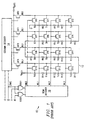
- FIG. 2 illustrates a schematic of a DAC 20 according to a first inventive embodiment.
- DAC 20 includes many components that are comparable in connection and operation to components in DAC 10 of Figure 1. To illustrate these like components, they are shown with the same reference identifiers as in Figure 1, with the exception that an apostrophe is added to the identifier in Figure 2. Briefly reviewing these comparable elements of DAC 20, and assuming the reader is familiar with DAC 10, DAC 20 is a 4-to-16 DAC that receives a 4-bit input word I0'-I3'.
- DAC 20 includes a series-connected resistor string 12' in the form of a meander having fifteen resistive elements R0' through R14', formed by one of various techniques such as those known in the art and with an effort to ensure like resistance for each element.
- DAC 20 further includes a number of bit lines BL0' through BL3' as well as a number of word lines WL0' through WL3'. Each word line is connected to enable four corresponding switching transistors, thereby providing a total of sixteen such transistors ST0' through ST15'. Each bit line is accessed by a corresponding one of column access transistors CAT0' through CAT3'.
- V MAIN electrical access to a given tap voltage is achieved by row decoder 16' enabling a word line to enable its corresponding switching transistors, and column decoder 14' enables a gate of one of the column access transistors such that the tap voltage passes through a switching transistor to a bit line, and then through the enabled column access transistor to an output V MAIN .
- Decoders 14' and 16' respond to bits I0'-I3' of the digital input word in the same general manner as DAC 10, whereby the two MSBs control column decoder 14' and the two LSBs, along with the lsb of the MSBs, control row decoder 16' in combination with the logic provided by exclusive OR gates EOG0' and EOG1'.
- V MAIN is neither the sole nor the final analog output for DAC 20.
- DAC 20 is shown as a 4-bit DAC for purposes of comparison to DAC 10 of the prior art; however, as will be appreciated by the conclusion of this document, the present inventive aspects may be readily implemented in a DAC having a larger number of inputs and, hence, having a larger number of other components to accommodate those inputs (e.g., resistive elements, voltage taps, word lines, bit lines, and so forth).
- DAC 20 its additional circuitry includes a data storage, comparison, and boost circuit 22, a coarse voltage selector 24 and its related coarse voltage access transistors CVAT0 and CVAT1, a switch circuit 26, and op amps OA A and OA B .
- a data storage, comparison, and boost circuit 22 includes a coarse voltage selector 24 and its related coarse voltage access transistors CVAT0 and CVAT1, a switch circuit 26, and op amps OA A and OA B .
- Data storage, comparison, and boost circuit 22 is named as such based on three of its functions, which are briefly noted here in relation to circuit connections and which are presented later in greater detail.
- circuit 22 receives and stores a series of incoming data words on an input 23, where these words are shown by way of example in Figure 2 as D 0 through D 4 .
- circuit 22 makes comparisons between certain ones of those words where, in the preferred embodiment, the comparison is between every other word (e.g., D 2 and D 0 , or D 3 and D 1 ).
- circuit 22 provides a resulting boost signal BOOST to a coarse voltage selector 24.
- Circuit 22 also sequentially provides its received data to the inputs to column decoder 14' and exclusive OR gates EOG0' and EOG1'.
- Coarse voltage selector 24 may be constructed in various manners to achieve the functionality described in detail below. Briefly summarizing that functionality here by way of introduction, coarse voltage selector 24 responds to the BOOST signal from circuit 22 by enabling one of the accessible coarse voltage access transistors; in the case of DAC 20, which recall is a 4-bit DAC, then for reasons understood later there are two such coarse voltage access transistors CVAT0 or CVAT1 are accessible by coarse voltage selector 24, and either of those may be enabled by presenting an enabling voltage to the gate of one of those transistors.
- the drain of transistor CVAT0 is connected to tap T3' and the drain of transistor CVAT1 is connected to tap T11'.
- V COARSE coarse voltage output
- the sources of coarse voltage access transistors CVAT0 and CVAT1 are connected to a coarse voltage output, V COARSE and, thus, V COARSE may be one of two voltages corresponding to the drain voltages of coarse voltage access transistors CVAT0 and CVAT1.
- V COARSE may be one of two voltages corresponding to the drain voltages of coarse voltage access transistors CVAT0 and CVAT1.
- the coarse voltage access transistors are yet another example of such a device which would appear in greater number for a larger DAC.
- V COARSE may be one of 128 voltages corresponding to the drain voltages of the 128 coarse voltage access transistors.
- switch circuit 26 receives V COARSE as one of its inputs. Additionally, as shown in Figure 2, switch circuit 26 also receives V MAIN as another input. Given these inputs, switch circuit 26 includes sufficient circuitry to couple at one time one of its inputs to a first of its two outputs, while concurrently coupling the other of the inputs to a second of its two outputs. This functionality is detailed later, from which one skilled in the art may construct various circuits to achieve the desired operation. By way of introduction here, note that the outputs of circuit 26 are connected to corresponding inputs of op amps OA A and OA B , and each of those op amp inputs is connected to a respective output sampling capacitor C A and C B .
- circuit 26 may connect either input V MAIN or V COARSE to a first one of op amps OA A and OA B while concurrently connecting the other of those inputs to a second one of op amps OA A and OA B .
- these connections ultimately give rise to output signals from each of op amps OA A and OA B at respective outputs OUT A and OUT B .
- DAC 20 receives digital data words and converts them to corresponding analog voltages as is the case for other DAC technology. More specifically, however, DAC 20 provides three additional aspects. In one aspect, without two different row decoders, a two-channel output is provided, with the first channel being OUT A and the second channel being OUT B . Additionally, this dual channel operation is overlapping such that while one channel output is valid the other is being developed. As another aspect, DAC 20 determines an output voltage not solely in response to a digital input word, but instead in response to a comparison between that word and a prior word received by the DAC.
- DAC 20 uses a comparison between successive digital words and the output is charged in response to that comparison.
- successive is used to mean one digital word following another at some later point, but it is not limited to digital words which are immediately following one another.
- the settling time of the DAC output is reduced by increasing, or "boosting", the output charge voltage for one or more time periods and thereafter permitting the output voltage to settle toward the final and desired output level.
- Figure 3a illustrates a plot of output charge voltage versus time to contrast the operation of a typical prior art DAC output and that of the preferred embodiment as achieved using V MAIN and V COARSE . More particularly, Figure 3a illustrates two plots, one designated as PA for a prior art DAC, and another designated INV corresponding to the present inventive embodiments. The plots indicate output voltage in the vertical dimension and time, shown in units of RC time constants, in the horizontal dimension. While the plots are not necessarily drawn to an exact scale, they generally depict, for both a prior art and inventive DAC, the rise of an output analog charge signal in response to an input digital word. For purposes of reference, this rise is shown from a first level V INIT to a final output, V F .
- V F is a level that is acceptably close to the ultimate output analog voltage asymptote given the RC load on the charge voltage.
- the preferred embodiment reaches V F in a lesser amount of time (i.e., at an increased speed).
- This preferred operation is achieved in part by charging a corresponding one of the charge capacitors connected to either of op amps OA A and OA B first with a "boosted" voltage, meaning a voltage that has an asymptote beyond V F .
- a "boosted" voltage meaning a voltage that has an asymptote beyond V F .
- the preferred embodiment output capacitor charges faster than the prior art case where it is charged only toward the value of V F .
- the boosted voltage is used to select from the resistor meander a "coarse" (i.e., estimated) voltage corresponding to the boosted voltage and, hence, this estimate is provided by V COARSE to switch circuit 26.
- switch circuit 26 may then charge one of the charge capacitors C A or C B using V COARSE .
- the same methodology just described as occurring between t 0 and t 1 is repeated for one or more additional time periods, where in each consecutive time period the level of boost is reduced so that the output charging voltage is reduced in magnitude relative to the immediately preceding period, but further where that asymptote is still beyond that of V F .
- the charge voltage still has a larger asymptote, and hence a steeper slope, than plot PA between t 1 and t 2 , but the charge voltage has a lesser slope (and asymptotic maximum) then the charge between t 0 and t 1 .
- this boosted voltage is used to select a coarse voltage to charge the output sampling capacitor between t 1 and t 2 . This process may again repeat, such as shown between t 2 and t 3 .
- the charge voltage connected to an output sampling capacitor is refined by setting that voltage equal to V F .
- this operation is achieved by switch circuit 26 changing its input so that V MAIN is now connected to the sampling capacitor that immediately before was connected to V COARSE . In Figure 3a, this occurs at t 3 . Accordingly, after some additional charge period, such as shown between t 3 and t 4 , the final output voltage V F is then reached (or nearly reached as it is approached in the sense of an asymptote) and hence a valid output signal is available for sampling from the output of the op amp corresponding to the charged sampling capacitor.
- Figure 3b again illustrates a plot of INV from Figure 3a but here in greater detail to further introduce two of the preferred embodiment aspects described above, namely, using a comparison of successive digital words to drive the output of DAC 20 and using a boosted value to drive that output.
- Figure 3b illustrates in the vertical dimension various voltage levels, where a first digital word D X is represented as is a successive digital word D X+1 .
- the horizontal dimension in Figure 3b illustrates time, and is further divided into time constants in increments of "RC," where RC is the time constant imposed on a tap in DAC 20.
- RC time constant imposed on a tap in DAC 20.
- DAC 20 determines a difference, designated in this document as ⁇ , between the digital words at issue (i.e., here, D X and D X+1 ). This difference is then used to generate an output that ultimately will settle to D X+1 , but which initially will charge toward an asymptote beyond D X+1 .
- the difference ⁇ is "boosted,” that is, it is increased by a boost factor B, and the increased result is used for multiple periods prior to providing an output merely equal to D X+1 .
- the length of each period differs as does its corresponding boost factor, as shown by the varying signals in Figure 3b, as detailed immediately below.
- the first boosting period is 0.5RC long and uses a boost factor equal to equal to 2 to determine an asymptotic charging level for the first period, illustrated in Figure 3b as BOOST 1 . This is shown in Figure 3b between t 0 and t 1 .
- the product of 2 ⁇ is added to the value of D X . This operation is perhaps better understood by way of a numeric example; accordingly, assume that D X equals decimal 5 and D X+1 equals decimal 13.
- DAC 20 has determined an asymptotic value that is 2 ⁇ greater than the current value of D X , which in the present case is 21.
- DAC 20 uses the result to select a voltage for V COARSE and that V COARSE is output and used to charge the output toward BOOST 1 as shown between t 0 and t 1 .
- a new boosting period is commenced and, therefore, the output is charged toward a new asymptote; however, to complete the illustration with respect to the first boosting period, then after t 1 a line is shown in phantom illustrating that the value of V COARSE used between t 0 and t 1 , if extended beyond t 1 , would approach the asymptote defined by BOOST 1 .
- the second boosting period is shown in Figure 3b between t 1 and t 2 , during which a second boost factor equal to 1.5 is multiplied times ⁇ , and then added to the value of D X , thereby providing an asymptote of BOOST 2 during this period.
- the second boosting period is 1.0RC long. Accordingly, during this second boosting period, the output is charged toward the asymptote of BOOST 2 .
- a third boosting period is shown in Figure 3b between t 2 and t 3 , during which a third boost factor equal to 1.25 is multiplied times ⁇ , and then added to the value of D X , thereby providing an asymptote of BOOST 3 during this period.
- the third boosting period is 2.5RC long.
- the output is charged toward the asymptote of BOOST 3 . Since the third boosting period is 2.5RC long, then during this time the output does not reach BOOST 3 , but to demonstrate the asymptotic behavior of the charging level during the third boosting period the charge level is extended in phantom to demonstrate that the charge level eventually would approach BOOST 3 .
- Figure 3b illustrates in the same manner as Figure 3a that after t 3 V MAIN is connected to the sampling capacitor that immediately before was connected to V COARSE .
- the final output voltage V F will reach that of the successive digital word D X+1 in the sense of an asymptote.
- this final period also will accommodate for any variance in the value of RC. More particularly, recall that the duration of each of the boosting periods is based on RC, which is the time constant imposed on a tap in DAC 20.
- the charged output voltage at t 3 may still be some distance from the value of D X+1 .
- the final period after t 3 will correct this distance by causing the output to settle toward the value of D X+1 .
- the asymptote is beyond D X+1 when considered from a direction relative to the previous digital word, D X .
- the second boosting period e.g., 0.5RC
- the third boosting period e.g., 2.0RC
- the output is allowed to settle to a value equal to D X+1 .
- successively increasing or successively decreasing words they have in common a sequence of boosting periods, where in the boosting period the direction (i.e., either up or down) of the level of boost matches the relative value from the first word to the successive word.
- the boosting asymptotes are upward and greater than the successive word.
- the successive word is less than the first word, then the boosting asymptotes are downward and less than the successive word. In either case, therefore, for each boosting period the difference between the asymptote and the first word is greater than the difference between the successive word and the first word.
- Figure 4 illustrates a block diagram showing greater detail within data storage, comparison, and boost circuit 22 of Figure 2.
- circuit 22 includes two storage circuits 28 and 30 for receiving pairs of incoming successive data words, where in the preferred embodiment the pairings are such that alternating words are directed to alternating ones of storage circuits 28 and 30.
- DAC 20 For a current example and to be used for the remainder of this document, assume after various digital words have been processed by DAC 20, then a sequence of 4-bit words D 0 , D 1 , D 2 , and D 3 are communicated to DAC 20.
- D 0 as the first word in the sequence, is directed to storage circuit 28 (shown in element 28a of storage circuit 28), while the next successive but alternating word, D 1 , is directed to the alternating storage circuit 30 (shown in element 30a of storage circuit 30).
- D 2 the third word in the succession, D 2 , once again is directed to an alternating one of the storage circuits and, hence, it is stored in element 28b of storage circuit 28.
- D 3 is directed to an alternating one of the storage circuits and, hence, it is stored in element 30b of storage circuit 30.
- subtraction circuit 32 provides the comparison function introduced earlier, that is, it provides a signal representative of alternately received successive digital input words.
- this comparison is the value introduced earlier as ⁇ , which equals the difference between the paired digital values stored in either of storage circuits 28 or 30. For example, when subtraction circuit 32 operates with respect to storage circuit 28, then ⁇ is the difference between D 2 and D 0 . Similarly, when subtraction circuit 32 operates with respect to storage circuit 30, then ⁇ is the difference between D 3 and D 1 .
- ⁇ relates to the difference between every other digital word received in the sequence of words. Once a value of ⁇ is determined, it is used to influence the ultimate output of DAC 20 by coupling it to boost circuit 36.
- Boost circuit 36 provides the changing slopes corresponding to the changing asymptotic charge levels illustrated between consecutively numbered time periods in Figures 3a and 3b.
- boost circuit 36 provides the three different periods of boosting introduced above, by providing an appropriate boost factor B which is multiplied times ⁇ , and where B decreases for each consecutive period.
- B boost factor
- the three levels of B correspond to a first level equal to 2, a second level equal to 1.5, and a third level equal to 1.25.
- a timing control circuit 37 controls the duration of each of these periods, that is, the duration that each boost level is multiplied times ⁇ , where recall here that the first time period equals 0.5RC, the second time period equals 1.0RC, and the third time period equals 2.5RC. Accordingly, the preceding descriptions should demonstrate to one skilled in the art that after a period equal to 4.0RC, the output is charged relatively close to V F .
- boost circuit 36 The product from boost circuit 36 is provided per period, and for each such period it is added via an adder 38 to the most recent digital word, which is thus shown in Figure 4 as D N-2 .
- this aspect involving the addition function applies to either the case where the successive word (D N ) is greater than the preceding word (D N-2 ), or where the successive word (D N ) is less than the preceding word (D N-2 ), and the function thereby produces a boosting asymptote that is properly positioned relative to D N-2 .
- the case where the successive word is greater than the preceding word should be relatively straightforward given the example set forth above. However, where the successive word is less than the preceding word, a few additional observations may be helpful.
- ⁇ will be negative number.
- D N-2 equals 13 and D N equals 5.
- adder 38 again adds the boosting product to D N-2 , but the boosting product will be a negative number thereby causing a subtraction of the absolute value of the boosting product from D N-2 .
- the resulting asymptote will be properly positioned by the boost factor (e.g., 2, 1.5, 1.25) relative to D N-2 .
- the asymptote value equals an asymptote that is
- the asymptote value equals an asymptote that is
- the asymptote value equals an asymptote that is
- the output of adder 38 provides the BOOST signal. Further, recall from the description of Figure 2 that in the preferred embodiment only half of the bit line address (i.e., the MSBs) are actually used from the BOOST signal to select V COARSE ; as a result and as further discussed below, the output of boost circuit 22 is shown to only provide bit 3 of BOOST (i.e., shown in Figure 4 as BOOST[3]).
- the preferred embodiment implements various specifics as described above, note that various alterations are also within the present inventive scope.
- the preceding describes three different periods of boosting the output charge with each period having a different duration.
- alternative embodiments may be created by modifying any one or more of the number of periods, the duration for each period, and the level of boost during a period.
- the preferred embodiment chooses V COARSE since it is readily obtained from voltage levels selected from the DAC resistor string.
- other boosting techniques may be developed within the present inventive scope given the inventive aspect of using successive DAC input data to provide the value of ⁇ .
- a spectrum of boosting techniques may be contemplated, where at one end of the spectrum is an implementation that charges over time a capacitance equal to the output sampling capacitor via a resistor to effectively model the RC load of the DAC while at the other end of the spectrum is an implementation that moves charge to a capacitance equal to the output sampling capacitor with an acceptable source of power.
- the illustration and description depicted above suggests boosting levels that create a signal that monotonically approaches the asymptote defined by the final data value (i.e., V F in Figure 3a).
- it may be preferred to implement a level of boosting so that during the charging process the output extends beyond the ultimate output voltage and then during one or more final periods it converges to the ultimate output voltage.
- first a value of 0.5 ⁇ is obtained by shifting the value of ⁇ once to the right (i.e., in effect, dividing by a factor of 2), and then the total of 1.5 ⁇ is achieved by adding the shifted result to the value of ⁇ .
- first a value of 0.25 ⁇ is obtained by shifting the value of ⁇ twice to the right (i.e., in effect, dividing by a factor of 2 2 ), and then the total of 1.25 ⁇ is achieved by adding the shifted result to the value of ⁇ .
- the boosted value is used to select a coarse voltage as detailed below, at which point it also will be apparent why only a portion of the boosted number (i.e., bit [3] in the example of Figure 2) is used in this manner.
- coarse voltage selector 24 is best appreciated in more detail by returning to Figure 2.
- the available levels of coarse voltages are dictated by the placement of coarse voltage access transistors CVAT0 and CVAT1.
- those transistors are located between each pair of bit lines.
- the preferred embodiment locates a number X/2 of coarse voltage access transistors, with each positioned between a corresponding pair of bit lines.
- Half of a binary number is defined by all bits other than the least significant bit of that number, which technically may be achieved by shifting the binary number once to the right, or simply disregarding its least significant bit.
- shifting those once to the right leaves only one MSB to select among the coarse voltage access transistors. For this reason, therefore, only bit [3] of the BOOST signal is connected from circuit 22 to selector 24. The value of this single bit, therefore causes either coarse voltage access transistor CVAT0 or CVAT1 to be selected.
- a greater number of MSBs are implemented, then one less than this larger number of bits are presented as the boosted signal to selector 24.
- bit position [3] value of 1 reaches coarse voltage selector 24 and, in response, it enables transistor CVAT1, thereby causing the voltage at tap T11' to be output as V COARSE to switch circuit 26, and thereby providing this voltage to charge the appropriate one of charge capacitors C A or C B .
- the above example of only two coarse voltages arises from the simplification that arises from the present example of a 16-bit DAC. In a more likely scenario, the DAC is considerably larger and, hence, so will be the number of available coarse voltages from which a selection may be made.
- Figure 5 illustrates a timing diagram of the operation of DAC 20, and it should be noted that exact timing and delays are not shown but instead the illustration presents a framework to demonstrate the general sequential and overlapping operations of various circuits.
- the diagram starts at a time designated t 10 , which is arbitrarily numbered to distinguish it from other time identifiers used earlier.
- t 10 assume for purposes of simplifying the present discussion that DAC 20 already has processed earlier digital input words, and has now stored the sequence of D 0 and D 2 , and D 1 and D 3 in storage circuits 28 and 30, respectively. Assume further that output signals for D 0 and D 1 also have already been provided.
- subtraction circuit 32 determines the value of ⁇ 1 equal to D 2 -D 0 .
- boost circuit 36 determines and outputs, with respect to ⁇ 1 , the three successive boost products corresponding to the boost factors of 2, 1.5, and 1.25, with each then added to the value of D 0 .
- these results correspond to the values shown in Figure 5 as B1, B2, and B3, respectively. Recall that in response to the two MSBs of the values, or at least in response to all but the least significant bit of those MSBs, a coarse voltage is selected by selector 24 and presented to switch circuit 26.
- switch circuit 26 connects V COARSE to charge sampling capacitor C A .
- V COARSE charge sampling capacitor C A
- t 13 and t 15 the boosted charging effect shown between t 0 and t 3 of Figures 3a-3b occurs.
- a coarse analog voltage charges capacitor C A in response to a boosted value relating to the difference between D 2 and D 0 .
- timing control circuit 37 enables passgate 34 so that D 2 is connected to inputs I0'-I3' of DAC 20.
- V MAIN As a result, the value of D 2 at this point is applied to the array in the same manner as described with respect to Figure 1, but here the driven output is V MAIN .
- switch circuit 26 connects V MAIN to charge sampling capacitor C A . Consequently, following t 16 , V MAIN completes the charge on charge capacitor C A from its existing value of V COARSE to a final value having V MAIN as its asymptote. In other words, V MAIN refines the value that resulted from the charge presented by V COARSE toward an ultimate settled value.
- the output of op amp OA A provides a valid analog voltage corresponding to D 2 . Accordingly, at this time, that analog voltage may be sampled at the op amp output and used for the appropriate purpose(s).
- t 4 is considerably earlier in time that the 12 time constants required of the prior art to reach the comparable V F level. From this, one skilled in the art will appreciate the greatly enhanced speed of operation of DAC 20 in comparison to the prior art.
- subtraction circuit 32 determines the value of ⁇ 2 equal to D 3 -D 1 .
- this operation overlaps the above-described operations which are then occurring relative to ⁇ 1 .
- boost circuit 36 determines and outputs, with respect to ⁇ 2 , the three successive boost products corresponding to the boost factors of 2, 1.5, and 1.25, and each of these is added to D 1 to form the results of shown in Figure 5 as B4, B5, and B6, respectively.
- the results relating to these values cause coarse voltage selector 24 to select an appropriate coarse voltage and present it as V COARSE to switch circuit 26.
- switch circuit 26 connects V COARSE to charge sampling capacitor C B .
- a boosted charging effect once more occurs, where here it relates to the value of ⁇ 2 , and is used to charge sampling capacitor CB.
- timing control circuit 37 enables passgate 34 so that D 3 is connected to inputs I0'-I3' of DAC 20 and, therefore, the value of D 3 is applied to the array to drive the value of V MAIN .
- switch circuit 26 connects V MAIN to charge sampling capacitor C B .
- the preferred embodiment further increases the charge speed by reducing effective capacitance during the periods when V COARSE is charging the output.
- a further modification to DAC 20 would be to add a non-complex voltage buffer between the sources of coarse voltage access transistors CVAT0 and CVAT1 and V COARSE . Such a buffer would further reduce the effect of any larger output capacitance such as the capacitance of sampling capacitor C A and C B . While this buffer may add a slight offset voltage to V COARSE , the effect of such a voltage on the ultimate output would be nullified during the final charging phase when the output is instead charged by V MAIN .
- the above embodiments provide numerous advantages over the prior art, many of which have been set forth above and additional ones of which will be ascertained by one skilled in the art.
- the preferred DAC provides a dual output without requiring a second row decoder, and the output charge times are considerably faster than other prior art DAC configurations.
- the dual output nature doubles the device bandwidth while the additional circuitry to achieve this capacity does not double the total spatial requirements of the device.
- various substitutions, modifications or alterations could be made to the descriptions set forth above without departing from the inventive scope. Indeed, some of these type of variations have been set forth above, and still others may be ascertained.
- Figure 2 demonstrates a location of coarse access voltage transistors between bit lines, an alternative location could be implemented, as could a larger number of such transistors to provide a greater number of coarse voltages for selection.
- DAC 20 has been shown to have a single input, dual inputs also could be used, and with those inputs each digital word could be compared to the word that immediately preceded it with respect to its same correspond input.
- the preceding illustrations have shown a two channel DAC due to its enhanced output capability; nevertheless, many of the present inventive teachings may apply to a single channel DAC, or other multiple channel DAC, to increase its speed.
- a single channel DAC digital input words are stored by the DAC and the difference between successive words which immediately follow one another, rather than alternating words, are used to generate a differential voltage from which a corresponding output analog voltage may be provided.
- the methodology of tailoring the differential voltage to first begin with a boosted coarse voltage component and then refining that voltage component with a main voltage component also may be implemented in a single channel DAC.
- the present inventive teachings also may be applied to a fully-differential configuration, such as of the type shown in U.S.
- the illustrations have been directed to a DACs with four inputs, the present teachings apply equally to DAC having greater or lesser input/output capacities.
Landscapes
- Engineering & Computer Science (AREA)
- Theoretical Computer Science (AREA)
- Analogue/Digital Conversion (AREA)
Abstract
Description
types of electronic circuits, or itself may be formed in a single integrated circuit device. In operation, the DAC is used to convert an input digital signal to an output analog signal, typically where the amplitude of the output analog signal corresponds directly to the magnitude of the input digital signal. For further background, a DAC illustrated as having a resistor string in a single dimension may be seen in co-pending U.S. Patent Application 09/342,878, (Docket TI-26740), entitled "Bit Interpolation In A Resistor String Digital-To-Analog Converter", filed June 29, 1999, having the same inventors as the present application, and hereby incorporated herein by reference. However, the embodiments of this application pertain more favorably to a DAC having a meander resistor string and, thus, a description of a prior art system with such a string is described as further background immediately below.
one of the accessible coarse voltage access transistors; in the case of
Claims (20)
- A digital to analog converter, comprising:an input for receiving a plurality of successive digital words;circuitry for storing the plurality of successive digital words;a string of series connected resistive elements, wherein the string comprises a plurality of voltage taps;an output for providing an analog output voltage corresponding to a selected one of the plurality of successive digital words;comparison circuitry for comparing the selected one and an earlier received one of the plurality of successive digital words; andcircuitry for generating the analog output voltage in response to the comparison circuitry.
- The converter of Claim 1 wherein the comparison comprises circuitry for forming a difference comparison by subtracting the earlier received one of the plurality of successive digital words from the selected one of the plurality of successive digital words.
- The converter of Claim 2 wherein the circuitry for generating the analog output voltage comprises circuitry for first coupling a first voltage to charge an output capacitance in response to the difference comparison.
- The converter of Claim 3 wherein the circuitry for coupling the first output voltage to charge the output capacitance in response to the difference comparison charges the output capacitance in response to a boosted value equal to a multiple of the difference comparison.
- The converter of Claim 3:
wherein the first voltage is provided by a selected one of the plurality of voltage taps; and
wherein the selected one of the plurality of voltage taps is selected in response to the difference comparison. - The converter of Claim 3, 4, or 5:
wherein the circuitry for generating the analog output voltage further comprises circuitry for second coupling a second voltage to further charge the output capacitance; and
wherein the analog output voltage is responsive to the first voltage and the second voltage coupled to the output capacitance. - The converter of Claim 6 wherein the circuitry for coupling the second output voltage to charge the output capacitance charges the output capacitance in response to a boosted value equal to a multiple of the difference comparison.
- The converter of Claim 6 or 7:
wherein the second voltage is provided by a selected one of the plurality of voltage taps; and
wherein the selected one of the plurality of voltage taps is selected in response to the difference comparison. - The converter of any one of the previous claims, wherein the comparison circuitry compares the selected one and the earlier received one of the plurality of successive digital words by forming a difference comparison by subtracting a digital representation of the earlier received one of the plurality of successive digital words from a digital representation of the selected one of the plurality of successive digital words.
- The converter of Claim 9 wherein the circuitry for generating the analog output voltage in response to the comparison circuitry comprises:circuitry for selecting a voltage at one of the plurality of voltage taps in response to the difference comparison; andcircuitry for coupling the selected voltage to charge an output capacitance to form the analog output voltage.
- The converter of Claim 10 wherein the circuitry for selecting selects the voltage at one of the plurality of voltage taps in response to a product equal to a boost factor times the difference comparison.
- The converter of any one of the previous claims:
wherein the output comprises a first output for providing a first analog output voltage;and further comprising a second output for providing a second analog output voltage. - The converter of Claim 12 wherein the selected one and the earlier received one of the plurality of successive digital words comprise alternately received digital words.
- The converter of any one of the previous claims wherein the circuitry for generating the analog output voltage in response to the comparison circuitry comprises, for each of a plurality of time periods:circuitry for selecting a corresponding voltage at one of the plurality of voltage taps in response to the difference comparison; andcircuitry for coupling each selected corresponding voltage to charge an output capacitance to form the analog output voltage.
- The converter of Claim 44 wherein the circuitry for selecting selects, for each of the plurality of time periods, the corresponding voltage at one of the plurality of voltage taps in response to a product equal to a boost factor times the difference comparison.
- The converter of Claim 14 wherein the plurality of time periods equals three time periods.
- The converter of Claim 14:
wherein each of the plurality of voltage taps is loaded with an estimated RC load; and
wherein each of the plurality of time periods has a duration relating to the estimated RC load. - The converter of any one of the previous claims wherein the circuitry for generating the analog output voltage comprises:circuitry for first coupling a first voltage to charge an output capacitance in response to the difference comparison, wherein the first voltage is selected from a group of taps that are a subset of the plurality of voltage taps;circuitry for second coupling a second voltage to further charge the output capacitance, wherein the second voltage is provided by a selected one of the plurality of voltage taps; and
wherein the analog output voltage is responsive to the first voltage and the second voltage coupled to the output capacitance. - The converter of Claim 18:
wherein the string of series connected resistive elements form a number of bit lines; and
wherein the group of taps has a number of taps equal to half the number of bit lines. - A digital to analog converter, comprising:an input for receiving a plurality of successive digital words;circuitry for storing the plurality of successive digital words;a string of series connected resistive elements, wherein the string comprises a plurality of voltage taps;an output for providing an analog output voltage corresponding to a selected one of the plurality of successive digital words;comparison circuitry for comparing the selected one and an earlier received one of the plurality of successive digital words;circuitry for generating the analog output voltage in response to the comparison circuitry by forming a difference comparison by subtracting the earlier received one of the plurality of successive digital words from the selected one of the plurality of successive digital words;
wherein the circuitry for generating the analog output voltage comprises:wherein the analog output voltage is responsive to the first voltage and the second voltage and the third voltage.circuitry for first coupling a first voltage to charge an output capacitance in response to the difference comparison;circuitry for second coupling a second voltage to further charge the output capacitance;circuitry for second coupling a third voltage to further charge the output capacitance;
Applications Claiming Priority (2)
| Application Number | Priority Date | Filing Date | Title |
|---|---|---|---|
| US386260 | 1999-08-31 | ||
| US09/386,260 US6222474B1 (en) | 1999-08-31 | 1999-08-31 | Resistor string digital-to-analog converter with boosted control based on differential input between successively received input words |
Publications (2)
| Publication Number | Publication Date |
|---|---|
| EP1081862A2 true EP1081862A2 (en) | 2001-03-07 |
| EP1081862A3 EP1081862A3 (en) | 2003-08-13 |
Family
ID=23524849
Family Applications (1)
| Application Number | Title | Priority Date | Filing Date |
|---|---|---|---|
| EP00306999A Withdrawn EP1081862A3 (en) | 1999-08-31 | 2000-08-16 | Digital-to-analog converter |
Country Status (3)
| Country | Link |
|---|---|
| US (1) | US6222474B1 (en) |
| EP (1) | EP1081862A3 (en) |
| JP (1) | JP2001094427A (en) |
Families Citing this family (7)
| Publication number | Priority date | Publication date | Assignee | Title |
|---|---|---|---|---|
| KR100456830B1 (en) * | 2002-10-22 | 2004-11-10 | 삼성전자주식회사 | Transistor array and layout method of this array |
| US6937180B1 (en) * | 2004-04-26 | 2005-08-30 | Texas Instruments Incorporated | Code-controlled voltage divider |
| WO2010079530A1 (en) * | 2009-01-07 | 2010-07-15 | 株式会社アドバンテスト | Circuit and method for digital-analog conversion |
| US8773887B1 (en) * | 2011-05-25 | 2014-07-08 | Peter K. Naji | Resistive memory devices and related methods |
| US9892782B1 (en) | 2011-05-25 | 2018-02-13 | Terra Prime Technologies, Llc | Digital to analog converters and memory devices and related methods |
| US9589633B2 (en) | 2011-05-25 | 2017-03-07 | Peter K. Nagey | Memory devices and related methods |
| KR101879331B1 (en) * | 2017-03-08 | 2018-07-18 | 충북대학교 산학협력단 | Folded resistor string DAC for the dual-output |
Family Cites Families (8)
| Publication number | Priority date | Publication date | Assignee | Title |
|---|---|---|---|---|
| JPS62155622A (en) * | 1985-12-27 | 1987-07-10 | Advantest Corp | Digital-analog converter |
| US4684922A (en) * | 1986-01-15 | 1987-08-04 | Analog Devices, Inc. | Temporal averaging using a voltage mode D/A converter |
| JP3134403B2 (en) * | 1991-09-09 | 2001-02-13 | オンキヨー株式会社 | Digital / analog converter |
| JP3162571B2 (en) * | 1994-04-28 | 2001-05-08 | 株式会社東芝 | D / A conversion circuit and A / D conversion circuit using the same |
| TW332356B (en) | 1994-10-21 | 1998-05-21 | At & T Corp | Integrated circuit having equivalent resistor string |
| JPH11284514A (en) * | 1998-01-27 | 1999-10-15 | Matsushita Electric Ind Co Ltd | D / A converter and method |
| JP3779056B2 (en) * | 1998-01-30 | 2006-05-24 | 富士通株式会社 | Voltage generation circuit and D / A conversion circuit |
| US6127957A (en) * | 1999-06-29 | 2000-10-03 | Texas Instruments Incorporated | Data converter with horizontal diffusion resistor meander |
-
1999
- 1999-08-31 US US09/386,260 patent/US6222474B1/en not_active Expired - Lifetime
-
2000
- 2000-08-16 EP EP00306999A patent/EP1081862A3/en not_active Withdrawn
- 2000-08-30 JP JP2000260770A patent/JP2001094427A/en not_active Abandoned
Also Published As
| Publication number | Publication date |
|---|---|
| US6222474B1 (en) | 2001-04-24 |
| EP1081862A3 (en) | 2003-08-13 |
| JP2001094427A (en) | 2001-04-06 |
Similar Documents
| Publication | Publication Date | Title |
|---|---|---|
| EP1257060B1 (en) | Digital-to-analogue converter using an array of current sources | |
| US4831381A (en) | Charge redistribution A/D converter with reduced small signal error | |
| KR100284959B1 (en) | Switched Capacitor Digital-to-Analog Converter | |
| US7511465B2 (en) | Digital pulse width modulated power supply with variable LSB | |
| JP4806439B2 (en) | D / A converter | |
| US20030179124A1 (en) | Analog to digital converter | |
| US7986256B2 (en) | A/D converter | |
| US5028926A (en) | Successive type analog-to-digital converter with a variable reference voltage for the digital to analog converter | |
| US6222474B1 (en) | Resistor string digital-to-analog converter with boosted control based on differential input between successively received input words | |
| US12592716B2 (en) | Adaptive power tuning in a successive approximation analog-to-digital converter | |
| JPS6161578B2 (en) | ||
| US4872011A (en) | Plural stage switched capacitor integrating digital-to-analog converter | |
| JP3361848B2 (en) | Apparatus for generating a digital signal output representative of a received analog signal | |
| CN111801894B (en) | Digital-to-analog converter system | |
| EP0743758B1 (en) | Quadratic digital/analog converter | |
| US4684924A (en) | Analog/digital converter using remainder signals | |
| JP3162571B2 (en) | D / A conversion circuit and A / D conversion circuit using the same | |
| US6927723B2 (en) | A/D converter and A/D conversion method | |
| US5929798A (en) | High speed and low power digital/analog (D/A) converter using dual current cell arrays | |
| US5760730A (en) | Method and system for analog-to-digital signal conversion with simultaneous analog signal compression | |
| KR100623343B1 (en) | regulator | |
| US7646321B2 (en) | Digital/analog converter | |
| JP2001517415A (en) | Driver circuit and method for low voltage operation of a continuous approximation register (SAR) analog / digital (A / D) converter | |
| US20080309538A1 (en) | Digital/analog converting driver and method | |
| KR20070048540A (en) | Digital-to-analog converting driver and digital-to-analog converting method combining resistive string converters and capacitor converters |
Legal Events
| Date | Code | Title | Description |
|---|---|---|---|
| PUAI | Public reference made under article 153(3) epc to a published international application that has entered the european phase |
Free format text: ORIGINAL CODE: 0009012 |
|
| AK | Designated contracting states |
Kind code of ref document: A2 Designated state(s): AT BE CH CY DE DK ES FI FR GB GR IE IT LI LU MC NL PT SE |
|
| AX | Request for extension of the european patent |
Free format text: AL;LT;LV;MK;RO;SI |
|
| PUAL | Search report despatched |
Free format text: ORIGINAL CODE: 0009013 |
|
| AK | Designated contracting states |
Designated state(s): AT BE CH CY DE DK ES FI FR GB GR IE IT LI LU MC NL PT SE |
|
| AX | Request for extension of the european patent |
Extension state: AL LT LV MK RO SI |
|
| 17P | Request for examination filed |
Effective date: 20040206 |
|
| AKX | Designation fees paid |
Designated state(s): DE FR GB IT NL |
|
| 17Q | First examination report despatched |
Effective date: 20050214 |
|
| STAA | Information on the status of an ep patent application or granted ep patent |
Free format text: STATUS: THE APPLICATION IS DEEMED TO BE WITHDRAWN |
|
| 18D | Application deemed to be withdrawn |
Effective date: 20050825 |