EP1080454B2 - Zugriffsgeschützter datenträger - Google Patents
Zugriffsgeschützter datenträger Download PDFInfo
- Publication number
- EP1080454B2 EP1080454B2 EP99924992.3A EP99924992A EP1080454B2 EP 1080454 B2 EP1080454 B2 EP 1080454B2 EP 99924992 A EP99924992 A EP 99924992A EP 1080454 B2 EP1080454 B2 EP 1080454B2
- Authority
- EP
- European Patent Office
- Prior art keywords
- operations
- execution
- data
- subset
- order
- Prior art date
- Legal status (The legal status is an assumption and is not a legal conclusion. Google has not performed a legal analysis and makes no representation as to the accuracy of the status listed.)
- Expired - Lifetime
Links
Images
Classifications
-
- H—ELECTRICITY
- H04—ELECTRIC COMMUNICATION TECHNIQUE
- H04L—TRANSMISSION OF DIGITAL INFORMATION, e.g. TELEGRAPHIC COMMUNICATION
- H04L9/00—Cryptographic mechanisms or cryptographic arrangements for secret or secure communications; Network security protocols
- H04L9/002—Countermeasures against attacks on cryptographic mechanisms
- H04L9/003—Countermeasures against attacks on cryptographic mechanisms for power analysis, e.g. differential power analysis [DPA] or simple power analysis [SPA]
-
- G—PHYSICS
- G06—COMPUTING OR CALCULATING; COUNTING
- G06F—ELECTRIC DIGITAL DATA PROCESSING
- G06F21/00—Security arrangements for protecting computers, components thereof, programs or data against unauthorised activity
- G06F21/70—Protecting specific internal or peripheral components, in which the protection of a component leads to protection of the entire computer
- G06F21/71—Protecting specific internal or peripheral components, in which the protection of a component leads to protection of the entire computer to assure secure computing or processing of information
- G06F21/75—Protecting specific internal or peripheral components, in which the protection of a component leads to protection of the entire computer to assure secure computing or processing of information by inhibiting the analysis of circuitry or operation
- G06F21/755—Protecting specific internal or peripheral components, in which the protection of a component leads to protection of the entire computer to assure secure computing or processing of information by inhibiting the analysis of circuitry or operation with measures against power attack
-
- G—PHYSICS
- G06—COMPUTING OR CALCULATING; COUNTING
- G06F—ELECTRIC DIGITAL DATA PROCESSING
- G06F21/00—Security arrangements for protecting computers, components thereof, programs or data against unauthorised activity
- G06F21/70—Protecting specific internal or peripheral components, in which the protection of a component leads to protection of the entire computer
- G06F21/71—Protecting specific internal or peripheral components, in which the protection of a component leads to protection of the entire computer to assure secure computing or processing of information
- G06F21/77—Protecting specific internal or peripheral components, in which the protection of a component leads to protection of the entire computer to assure secure computing or processing of information in smart cards
-
- G—PHYSICS
- G06—COMPUTING OR CALCULATING; COUNTING
- G06K—GRAPHICAL DATA READING; PRESENTATION OF DATA; RECORD CARRIERS; HANDLING RECORD CARRIERS
- G06K19/00—Record carriers for use with machines and with at least a part designed to carry digital markings
- G06K19/06—Record carriers for use with machines and with at least a part designed to carry digital markings characterised by the kind of the digital marking, e.g. shape, nature, code
- G06K19/067—Record carriers with conductive marks, printed circuits or semiconductor circuit elements, e.g. credit or identity cards also with resonating or responding marks without active components
- G06K19/07—Record carriers with conductive marks, printed circuits or semiconductor circuit elements, e.g. credit or identity cards also with resonating or responding marks without active components with integrated circuit chips
- G06K19/073—Special arrangements for circuits, e.g. for protecting identification code in memory
- G06K19/07309—Means for preventing undesired reading or writing from or onto record carriers
- G06K19/07363—Means for preventing undesired reading or writing from or onto record carriers by preventing analysis of the circuit, e.g. dynamic or static power analysis or current analysis
-
- G—PHYSICS
- G07—CHECKING-DEVICES
- G07F—COIN-FREED OR LIKE APPARATUS
- G07F7/00—Mechanisms actuated by objects other than coins to free or to actuate vending, hiring, coin or paper currency dispensing or refunding apparatus
- G07F7/08—Mechanisms actuated by objects other than coins to free or to actuate vending, hiring, coin or paper currency dispensing or refunding apparatus by coded identity card or credit card or other personal identification means
- G07F7/0806—Details of the card
- G07F7/0813—Specific details related to card security
- G07F7/082—Features insuring the integrity of the data on or in the card
-
- G—PHYSICS
- G07—CHECKING-DEVICES
- G07F—COIN-FREED OR LIKE APPARATUS
- G07F7/00—Mechanisms actuated by objects other than coins to free or to actuate vending, hiring, coin or paper currency dispensing or refunding apparatus
- G07F7/08—Mechanisms actuated by objects other than coins to free or to actuate vending, hiring, coin or paper currency dispensing or refunding apparatus by coded identity card or credit card or other personal identification means
- G07F7/10—Mechanisms actuated by objects other than coins to free or to actuate vending, hiring, coin or paper currency dispensing or refunding apparatus by coded identity card or credit card or other personal identification means together with a coded signal, e.g. in the form of personal identification information, like personal identification number [PIN] or biometric data
- G07F7/1008—Active credit-cards provided with means to personalise their use, e.g. with PIN-introduction/comparison system
-
- G—PHYSICS
- G06—COMPUTING OR CALCULATING; COUNTING
- G06Q—INFORMATION AND COMMUNICATION TECHNOLOGY [ICT] SPECIALLY ADAPTED FOR ADMINISTRATIVE, COMMERCIAL, FINANCIAL, MANAGERIAL OR SUPERVISORY PURPOSES; SYSTEMS OR METHODS SPECIALLY ADAPTED FOR ADMINISTRATIVE, COMMERCIAL, FINANCIAL, MANAGERIAL OR SUPERVISORY PURPOSES, NOT OTHERWISE PROVIDED FOR
- G06Q20/00—Payment architectures, schemes or protocols
- G06Q20/30—Payment architectures, schemes or protocols characterised by the use of specific devices or networks
- G06Q20/34—Payment architectures, schemes or protocols characterised by the use of specific devices or networks using cards, e.g. integrated circuit [IC] cards or magnetic cards
- G06Q20/341—Active cards, i.e. cards including their own processing means, e.g. including an IC or chip
-
- H—ELECTRICITY
- H04—ELECTRIC COMMUNICATION TECHNIQUE
- H04L—TRANSMISSION OF DIGITAL INFORMATION, e.g. TELEGRAPHIC COMMUNICATION
- H04L2209/00—Additional information or applications relating to cryptographic mechanisms or cryptographic arrangements for secret or secure communication H04L9/00
- H04L2209/08—Randomization, e.g. dummy operations or using noise
Definitions
- Data storage devices containing a chip are used in a wide variety of different applications, for example, for conducting financial transactions, paying for goods or services, or as a means of identification for controlling access or entry controls.
- confidential data is usually processed within the data storage device's chip, which must be protected from access by unauthorized third parties. This protection is ensured, among other things, by the fact that the chip's internal structures are very small, making it very difficult to access these structures in order to spy on the data processed within them.
- the chip can be embedded in a very firmly adhering compound, the forcible removal of which destroys the semiconductor chip or at least destroys the secret data stored therein. It is also possible to provide the semiconductor chip with a protective layer during its manufacture, which cannot be removed without destroying the semiconductor chip.
- a data storage device with a semiconductor chip which has at least one memory in which an operating program containing several commands is stored. Each command generates signals detectable from outside the semiconductor chip. The signals are measured by the current consumption at the terminals of the integrated circuit, which allows conclusions to be drawn about the processed data.
- a protective circuit is provided that generates a pseudo-random sequence using simulation cells. The current behavior, which is measurable from the outside, is thus superimposed with a random signal.
- EP 0 908 810 A2 discloses a device for processing program information structured as sequences of blocks.
- the device comprises a secure circuit with a CPU, an external memory, and a buffer memory.
- a sequence of blocks of program information from the external memory to the buffer memory, the order of the transferred blocks within the sequence is randomly varied.
- the invention is based on the object of protecting secret data contained in the chip of a data carrier from unauthorized access.
- the inventive solution does not take any measures to prevent the exposure of the chip's internal structures or the attachment of microprobes. Instead, measures are taken to make it more difficult for a potential attacker to draw conclusions about secret information from any intercepted signal waveforms.
- the signal waveforms depend on the operations the chip is currently performing. These operations are controlled using an operating program stored in the chip's memory.
- the operating program consists of a series of individual commands, each of which triggers a precisely defined operation. In order for the chip to perform its intended functions, a corresponding command sequence must be defined for each of these functions.
- One such function could be, for example, the encryption of data using a secret key.
- commands are preferably used to implement a desired function, or are used in such a way that spying on information is difficult or even impossible.
- no commands or command sequences should be used for which the processed data can be easily deduced by eavesdropping.
- the attack on the processed data can be made more difficult by using, for security-relevant operations, only those commands that trigger an identical or very similar signal sequence or commands for which the processed data has no or only a very small influence on the signal sequence.
- security-relevant operations are not carried out with genuine secret data, but with falsified secret data, from which the genuine secret data cannot be determined without the addition of additional secret information. This means that even if an attacker succeeds in determining the secret data used in an operation, they cannot cause any damage with it, since the intercepted data is not the genuine secret data but falsified secret data.
- the data storage device delivers correct results when used legitimately, despite the falsified secret data.
- This is achieved by first defining a function that falsifies the genuine secret data, for example, an EXOR operation of the secret data with a random number.
- the genuine secret data is falsified using the function thus defined. All operations on the data storage device are performed using the falsified secret data, which can subsequently compensate for the falsification of the secret data. In the case of EXOR-falsified secret data, these would be operations that are linear with respect to EXOR operations.
- the genuine secret data Before an operation is performed that does not allow such compensation, for example, an operation that is non-linear with respect to EXOR operations, the genuine secret data must be restored so that this operation is performed using the genuine secret data.
- the recovery of the genuine secret data after performing a compensable function is achieved, for example, by EXORing the function value determined using the falsified secret data with a corresponding function value of the random number used for the falsification.
- the above procedure results in the genuine secret data being used only for operations, such as non-linear operations, for which this is absolutely necessary, i.e., operations that cannot be performed with falsified secret data. Since such operations are generally very complex and not easily analyzed, it is extremely difficult, if not impossible, for a potential attacker to determine the genuine secret data by analyzing the signal patterns generated by these operations. Since the simply structured functions, for which subsequent compensation for the falsification is possible, are performed with falsified secret data, the described procedure makes it extremely difficult to determine the genuine secret data of the data carrier from unauthorized intercepted signal patterns.
- the signal patterns depend on the operations the chip is currently executing. If these operations are always executed according to the same rigid pattern, i.e., in particular, always in the same order, and the attacker knows this order, an attacker must overcome far fewer difficulties to spy on data than if they do not even know which operation is currently being processed at which time. Therefore, according to the invention, the processing of security-relevant operations within the chip card is to be as far removed as possible from a rigid sequence, thus offering the attacker as few starting points for analyzing the secret data as possible. This is achieved by executing as many operations as possible, ideally even all operations, which are independent of one another in the sense that each of the operations does not require data determined by the other operations, in a variable order, for example, random or dependent on input data.
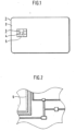
- a chip card 1 As an example of the data carrier, a chip card 1 is shown.
- the chip card 1 consists of a card body 2 and a chip module 3, which is inserted into a recess provided for this purpose in the card body 2.
- Essential components of the chip module 3 are contact surfaces 4, via which an electrical connection to an external device can be established, and a chip 5, which is electrically connected to the contact surfaces 4.
- a Fig. 1 A coil (not shown) or another transmission means for establishing a communication connection between the chip 5 and an external device may be present.
- Fig. 2 is a greatly enlarged section of chip 5 from Fig. 1 shown in top view.
- the special feature of the Fig. 2 is that the active surface of the chip 5 is shown, ie all layers that generally protect the active layer of the chip 5 are in Fig. 2 Not shown.
- the exposed structures 6 can be contacted with microprobes, for example.
- the microprobes are very thin needles that are brought into electrical contact with the exposed structures 6, for example, conductor tracks, using a precision positioning device.
- the signal patterns recorded with the microprobes are further processed with suitable measuring and evaluation devices with the aim of being able to draw conclusions about secret data on the chip.
- the invention ensures that even if an attacker succeeds in removing the protective layer of chip 5 without destroying the circuit and in contacting the exposed structures 6 of chip 5 with microprobes or otherwise intercepting them, it is very difficult or even impossible to gain access to, in particular, secret data on the chip.
- the invention also applies if an attacker gains access to the signal patterns of chip 5 by other means.
- the instructions or instruction sequences of the operating program of the chip are selected, at least for all security-relevant operations, in such a way that conclusions about the data processed with the instructions can either not be drawn at all or at least can only be drawn with great difficulty from the intercepted signal patterns.
- bit commands instead of bit commands, one can use byte commands, such as copy or rotate commands, which process an entire byte consisting of eight bits instead of a single bit.
- the byte command triggers a much more complex signal sequence, making it extremely difficult to associate individual bits with subsections of the signal sequence. This obscures the information processed with the byte command, thus making it more difficult to eavesdrop on this information.
- a set of safety-relevant commands can thus be composed of commands belonging to one or more of the above-mentioned variants.
- a command set can be used in which all commands belong to the same variant, although it may also be permitted for some or all commands to also belong to other variants. For example, only byte commands may be permitted, with preference given to commands that also trigger a very similar signal sequence.
- Security-relevant operations include, for example, encryption operations, which are also frequently used in chip cards.
- encryption operations which are also frequently used in chip cards.
- a series of individual operations are executed that result in bit-by-bit changes in a data word.
- all of these commands are replaced by byte commands and/or the other measures mentioned above are taken. This makes it even more difficult for an attacker to draw conclusions about the secret keys used in the encryption from the intercepted signal patterns, thus preventing misuse of these secret keys.
- Fig. 3 shows a schematic representation of a section of a functional sequence in the chip card.
- An encryption operation was chosen as an example for the illustration. However, the principles explained in this example are also applicable to any other security-relevant operations.
- data abc which can be in plain text or already encrypted, is fed to a node 7.
- the data abc is linked with a key K1. In the present example, this link is an EXOR link, but other suitable linking methods can also be used.
- a non-linear function g is then applied to the linking result in a function block 8.
- function block 8 represents a non-linear function, it is Fig. 3 in the form of a distorted rectangle.
- the data generated by function block 8 are, according to the second alternative to the invention, EXORed with a random number Z at a node 9 and then further processed in a function block 10.
- the data is falsified, which makes it difficult for an attacker to analyze the processes in function block 10, which represents a linear mapping using a function f.
- Fig. 3 an undistorted rectangle is used.
- the data generated in function block 10 is linked at a link point 11 with data f (Z) that was previously generated, for example, during card production by applying the function f to the random number Z. This link compensates for the corruption of the data with the random number Z at link point 9.
- the link at link point 11 with the data f(Z) and K2 can be made either with the individual components K2 and f(Z) or with the result of an EXOR operation of these individual components.
- the latter approach opens up the possibility that the key K2 does not have to be available in plaintext, but only the key K2 EXORed with f(Z). If this link value has already been calculated in advance, e.g., during the initialization or personalization of chip card 1 and stored in the card's memory, it is not necessary to store the key K2 in plaintext in chip card 1. In this way, the security of chip card 1 can be further increased.
- the procedure described, corresponding to the second alternative to the invention, can be summarized as follows: the data processed in the encryption operation are falsified, whenever possible, by EXOR operation with a random number Z in order to prevent the spying of secret data. Falsification is fundamentally possible for all functions f that exhibit linear behavior with respect to EXOR operations. For non-linear functions g, the unfalsified data must be used. It is therefore necessary that, before applying the non-linear function g to the data, the falsification is compensated for by an EXOR operation of the data with the function value f (Z).
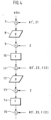
- Fig. 4 shows one of the Fig. 3 corresponding section of a functional sequence of a chip card for a further variant of the second alternative to the invention.
- the processing of the data abc is carried out in the same way as in Fig. 3 and will therefore not be explained again in the following.
- the corrupted keys K1', K2', and K3' are fed in together with the random numbers Z1, Z2, and Z3 required to compensate for the corruption, with the corrupted keys being fed in first, followed by the random numbers. This ensures that the correct keys K1, K2, and K3 do not appear at all.
- This procedure is particularly advantageous for encryption methods in which the keys K1, K2, and K3 are derived from a common key K.
- the key K falsified using the random number Z is stored in the chip card 1
- the random numbers Z1, Z2, and Z3 determined by applying the key derivation method to the random number Z are stored in the chip card 1.
- This storage must take place in a secure environment, for example, during the personalization phase of the chip card 1.
- the falsified derived keys K1', K2' and K3' are also required. These keys can then be derived from the falsified key K when needed. With this procedure, no operations are performed with the genuine key K or with the genuine derived keys K1, K2 and K3, so that spying on these keys is practically impossible. Since the derived random numbers Z1, Z2 and Z3 have already been determined in advance and stored in chip card 1, no further operations are performed with them that could be spied on by an attacker. Thus, access to the genuine derived keys K1, K2 and K3 by spying on the falsified derived keys K1', K2' and K3' is also not possible, since the derived random numbers Z1, Z2 and Z3 are required for this.
- random numbers Z and function values f (Z) are stored in the memory of the chip card.
- R and function values f (Z) it is also possible to store only a small number of random numbers R and function values f (Z) at a time and, whenever these values are needed, to determine new random numbers Z and function values f (Z) by EXOR operation or another suitable combination of several stored random numbers Z and function values F (Z).
- the random numbers Z for the EXOR operation can be randomly selected from the set of stored random numbers Z.
- the storage of the random numbers Z and function values f(Z) is omitted, as these are generated as needed using suitable generators. It is important that the generator(s) do not generate the function values f(Z) by applying the linear function f to the random number Z, but rather generate pairs of random numbers Z and function values f(Z) in another way, since otherwise, by eavesdropping on the application of the function f to the random number Z, this random number Z could possibly be spied on, and this information could be used to determine further secret data.
- all security-relevant data can be falsified using additional data, such as random numbers, and then subjected to further processing.
- additional data such as random numbers
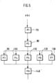
- Fig. 5 shows, to illustrate the invention, a schematic representation of the sequence in which some operations are processed by the chip card.
- Fig. 5 In particular, it is shown which operations must be processed sequentially by the chip card 1, as they depend on each other, and which operations can in principle be processed in parallel and thus in any order.
- Fig. 5 An excerpt from a program run of chip card 1 is shown, in which data abc is processed. All operations that must be processed sequentially are shown in Fig. 5 sequentially. All operations where the order of execution is not important are arranged in parallel.
- FIG. 5 The processing of data abc begins with an operation P1, which is represented in the form of a block 70. This block is followed sequentially by a block 80, which represents the operation P2. Fig. 5 This means that the processing sequence of operations P1 and P2 cannot be interchanged, ie it is absolutely fixed. After block 80, the program branches to Fig. 5 The diagram shown consists of five blocks 90, 100, 110, 120, 130, which represent the operations P3, P4, P5, P6 and P7. This means that the blocks P3, P4, P5, P6 and P7 can be processed simultaneously and can therefore also be processed in any order. According to the invention, the order in which these operations P3, P4, P5, P6, P7 are processed is varied with each run, i.e.
- operation P8 follows, the processing order of which is not variable. Operation P8 is represented by block 140. Operation P8 can be followed by further operations, both in variable order and in fixed order, which, however, are in the Fig. 5 are no longer shown.
- the invention can be used, for example, in the context of processing encryption algorithms that frequently contain similar operations whose processing sequence can be varied.
- the processing sequence can either be determined before the first variable operation jointly for all operations that can be interchanged with this first operation.
- the next operation to be processed is determined from the set of remaining variable operations. In both cases, random numbers can be used to determine the processing sequence.
Landscapes
- Engineering & Computer Science (AREA)
- Physics & Mathematics (AREA)
- Computer Security & Cryptography (AREA)
- General Physics & Mathematics (AREA)
- Computer Hardware Design (AREA)
- Theoretical Computer Science (AREA)
- General Engineering & Computer Science (AREA)
- Software Systems (AREA)
- Mathematical Physics (AREA)
- Microelectronics & Electronic Packaging (AREA)
- Computer Networks & Wireless Communication (AREA)
- Business, Economics & Management (AREA)
- Signal Processing (AREA)
- Accounting & Taxation (AREA)
- Strategic Management (AREA)
- General Business, Economics & Management (AREA)
- Storage Device Security (AREA)
- Control Of Vending Devices And Auxiliary Devices For Vending Devices (AREA)
Applications Claiming Priority (7)
| Application Number | Priority Date | Filing Date | Title |
|---|---|---|---|
| DE19822217.3A DE19822217B4 (de) | 1998-05-18 | 1998-05-18 | Zugriffsgeschützter Datenträger |
| DE19822218 | 1998-05-18 | ||
| DE19822220 | 1998-05-18 | ||
| DE19822220.3A DE19822220B4 (de) | 1998-05-18 | 1998-05-18 | Zugriffsgeschützter Datenträger |
| DE19822217 | 1998-05-18 | ||
| DE19822218.1A DE19822218B4 (de) | 1998-05-18 | 1998-05-18 | Zugriffsgeschützter Datenträger |
| PCT/EP1999/003385 WO1999060534A1 (de) | 1998-05-18 | 1999-05-17 | Zugriffsgeschützter datenträger |
Publications (3)
| Publication Number | Publication Date |
|---|---|
| EP1080454A1 EP1080454A1 (de) | 2001-03-07 |
| EP1080454B1 EP1080454B1 (de) | 2018-01-03 |
| EP1080454B2 true EP1080454B2 (de) | 2025-03-26 |
Family
ID=27218381
Family Applications (1)
| Application Number | Title | Priority Date | Filing Date |
|---|---|---|---|
| EP99924992.3A Expired - Lifetime EP1080454B2 (de) | 1998-05-18 | 1999-05-17 | Zugriffsgeschützter datenträger |
Country Status (8)
| Country | Link |
|---|---|
| US (2) | US8457302B1 (enExample) |
| EP (1) | EP1080454B2 (enExample) |
| JP (1) | JP4611523B2 (enExample) |
| CN (1) | CN1174347C (enExample) |
| AU (1) | AU4144399A (enExample) |
| CA (3) | CA2332350C (enExample) |
| ES (1) | ES2660057T3 (enExample) |
| WO (1) | WO1999060534A1 (enExample) |
Families Citing this family (14)
| Publication number | Priority date | Publication date | Assignee | Title |
|---|---|---|---|---|
| DE19837808A1 (de) * | 1998-08-20 | 2000-02-24 | Orga Kartensysteme Gmbh | Verfahren zur Ausführung eines Verschlüsselungsprogramms zur Verschlüsselung von Daten in einem mikroprozessorgestützten, tragbaren Datenträger |
| DE19841676A1 (de) * | 1998-09-11 | 2000-03-16 | Giesecke & Devrient Gmbh | Zugriffsgeschützter Datenträger |
| DE19963408A1 (de) * | 1999-12-28 | 2001-08-30 | Giesecke & Devrient Gmbh | Tragbarer Datenträger mit Zugriffsschutz durch Schlüsselteilung |
| DE19963407A1 (de) * | 1999-12-28 | 2001-07-12 | Giesecke & Devrient Gmbh | Tragbarer Datenträger mit Zugriffsschutz durch Nachrichtenverfremdung |
| FR2810138B1 (fr) * | 2000-06-08 | 2005-02-11 | Bull Cp8 | Procede de stockage securise d'une donnee sensible dans une memoire d'un systeme embarque a puce electronique, notamment d'une carte a puce, et systeme embarque mettant en oeuvre le procede |
| FR2820577B1 (fr) * | 2001-02-08 | 2003-06-13 | St Microelectronics Sa | Procede securise de calcul cryptographique a cle secrete et composant mettant en oeuvre un tel procede |
| DE10201441A1 (de) * | 2002-01-16 | 2003-08-14 | Infineon Technologies Ag | Schiebevorrichtung und Verfahren zum Verschieben |
| JP3881942B2 (ja) * | 2002-09-04 | 2007-02-14 | 松下電器産業株式会社 | 暗号化部を有する半導体装置 |
| US7631198B2 (en) * | 2005-05-10 | 2009-12-08 | Seagate Technology | Protocol scripting language for safe execution in embedded system |
| SG186618A1 (en) | 2007-12-03 | 2013-01-30 | Internat Frontier Tech Lab Inc | Authentication verifying method, authentication verifying member and authentication verifying member producing method |
| DE102010010851A1 (de) | 2010-03-10 | 2011-09-15 | Giesecke & Devrient Gmbh | Ausspähungsschutz bei der Ausführung einer Operationssequenz in einem tragbaren Datenträger |
| GB2494731B (en) * | 2011-09-06 | 2013-11-20 | Nds Ltd | Preventing data extraction by sidechannel attack |
| JP6280371B2 (ja) * | 2014-01-20 | 2018-02-14 | 株式会社東芝 | 携帯可能電子装置、電子回路および端末 |
| US9430676B1 (en) | 2015-03-17 | 2016-08-30 | Lenovo Enterprise Solutions (Singapore) Pte. Ltd. | Processor related noise encryptor |
Family Cites Families (33)
| Publication number | Priority date | Publication date | Assignee | Title |
|---|---|---|---|---|
| US4249180A (en) * | 1978-09-20 | 1981-02-03 | Northern Telecom Limited | Past dependent microcomputer cipher apparatus |
| GB2112190B (en) | 1981-12-23 | 1985-12-18 | Omron Tateisi Electronics Co | Personal identification system |
| JPS62134679A (ja) * | 1985-12-09 | 1987-06-17 | 松下電器産業株式会社 | 暗号文書作成読出装置 |
| JPS62190583A (ja) | 1986-02-17 | 1987-08-20 | Mitsubishi Electric Corp | 登録カ−ドを用いた個人識別システム |
| JPH01114995A (ja) * | 1987-10-29 | 1989-05-08 | Toppan Printing Co Ltd | Icカード |
| US5016274A (en) * | 1988-11-08 | 1991-05-14 | Silvio Micali | On-line/off-line digital signing |
| FR2638869B1 (fr) * | 1988-11-10 | 1990-12-21 | Sgs Thomson Microelectronics | Dispositif de securite contre la detection non autorisee de donnees protegees |
| JP2731945B2 (ja) * | 1989-06-05 | 1998-03-25 | エヌ・ティ・ティ・データ通信株式会社 | 個別鍵による認証が可能なicカード |
| FR2650458B1 (fr) * | 1989-07-25 | 1991-10-11 | Trt Telecom Radio Electr | Procede de traitement d'une permutation irreguliere de donnees protegees par chiffrement |
| US5003596A (en) * | 1989-08-17 | 1991-03-26 | Cryptech, Inc. | Method of cryptographically transforming electronic digital data from one form to another |
| CA2037857C (en) * | 1990-03-20 | 2001-01-16 | Roy Allen Griffin, Iii | Prevention of determination of time of execution of predetermined data processing routine in relation to occurrence of prior observable external event |
| US5655096A (en) | 1990-10-12 | 1997-08-05 | Branigin; Michael H. | Method and apparatus for dynamic scheduling of instructions to ensure sequentially coherent data in a processor employing out-of-order execution |
| JP2933180B2 (ja) * | 1991-04-25 | 1999-08-09 | 沖電気工業株式会社 | 暗証符号照合装置 |
| SE470001B (sv) * | 1991-09-12 | 1993-10-18 | Televerket | Förfarande för identifiering och kryptonyckelutbyte mellan två kommunicerande apparater för krypterad trafik |
| US5297201A (en) * | 1992-10-13 | 1994-03-22 | J.D. Technologies, Inc. | System for preventing remote detection of computer data from tempest signal emissions |
| US5655023A (en) * | 1994-05-13 | 1997-08-05 | Pitney Bowes Inc. | Advanced postage payment system employing pre-computed digital tokens and with enhanced security |
| US5606616A (en) * | 1995-07-03 | 1997-02-25 | General Instrument Corporation Of Delaware | Cryptographic apparatus with double feedforward hash function |
| JPH0973416A (ja) * | 1995-09-05 | 1997-03-18 | Dainippon Printing Co Ltd | Icカード |
| FR2745924B1 (fr) * | 1996-03-07 | 1998-12-11 | Bull Cp8 | Circuit integre perfectionne et procede d'utilisation d'un tel circuit integre |
| JPH09265516A (ja) * | 1996-03-29 | 1997-10-07 | Toshiba Corp | プリペイド用icカード処理装置 |
| US6226383B1 (en) * | 1996-04-17 | 2001-05-01 | Integrity Sciences, Inc. | Cryptographic methods for remote authentication |
| CA2177622A1 (en) * | 1996-05-29 | 1997-11-30 | Thierry Moreau | Cryptographic data integrity apparatus and method based on pseudo-random bit generators |
| US6373946B1 (en) * | 1996-05-31 | 2002-04-16 | Ico Services Ltd. | Communication security |
| US6337909B1 (en) * | 1996-10-10 | 2002-01-08 | Certicom Corp. | Generation of session keys for El Gamal-like protocols from low hamming weight integers |
| US6049613A (en) * | 1997-03-07 | 2000-04-11 | Jakobsson; Markus | Method and apparatus for encrypting, decrypting, and providing privacy for data values |
| US5991415A (en) * | 1997-05-12 | 1999-11-23 | Yeda Research And Development Co. Ltd. At The Weizmann Institute Of Science | Method and apparatus for protecting public key schemes from timing and fault attacks |
| US6122742A (en) * | 1997-06-18 | 2000-09-19 | Young; Adam Lucas | Auto-recoverable and auto-certifiable cryptosystem with unescrowed signing keys |
| US6061449A (en) * | 1997-10-10 | 2000-05-09 | General Instrument Corporation | Secure processor with external memory using block chaining and block re-ordering |
| AU2557399A (en) * | 1998-01-02 | 1999-07-26 | Cryptography Research, Inc. | Leak-resistant cryptographic method and apparatus |
| US7587044B2 (en) * | 1998-01-02 | 2009-09-08 | Cryptography Research, Inc. | Differential power analysis method and apparatus |
| JP4317607B2 (ja) * | 1998-12-14 | 2009-08-19 | 株式会社日立製作所 | 情報処理装置、耐タンパ処理装置 |
| DE19963408A1 (de) * | 1999-12-28 | 2001-08-30 | Giesecke & Devrient Gmbh | Tragbarer Datenträger mit Zugriffsschutz durch Schlüsselteilung |
| CA2329590C (en) * | 2000-12-27 | 2012-06-26 | Certicom Corp. | Method of public key generation |
-
1999
- 1999-05-17 ES ES99924992.3T patent/ES2660057T3/es not_active Expired - Lifetime
- 1999-05-17 JP JP2000550074A patent/JP4611523B2/ja not_active Expired - Lifetime
- 1999-05-17 AU AU41443/99A patent/AU4144399A/en not_active Abandoned
- 1999-05-17 CN CNB998082449A patent/CN1174347C/zh not_active Expired - Lifetime
- 1999-05-17 CA CA2332350A patent/CA2332350C/en not_active Expired - Lifetime
- 1999-05-17 CA CA2885956A patent/CA2885956C/en not_active Expired - Lifetime
- 1999-05-17 CA CA2885961A patent/CA2885961C/en not_active Expired - Lifetime
- 1999-05-17 EP EP99924992.3A patent/EP1080454B2/de not_active Expired - Lifetime
- 1999-05-17 WO PCT/EP1999/003385 patent/WO1999060534A1/de not_active Ceased
- 1999-05-17 US US09/700,656 patent/US8457302B1/en not_active Expired - Fee Related
-
2013
- 2013-05-23 US US13/901,262 patent/US9288038B2/en not_active Expired - Fee Related
Also Published As
| Publication number | Publication date |
|---|---|
| US8457302B1 (en) | 2013-06-04 |
| CA2885961C (en) | 2015-12-15 |
| AU4144399A (en) | 1999-12-06 |
| EP1080454A1 (de) | 2001-03-07 |
| CA2332350C (en) | 2015-07-07 |
| JP4611523B2 (ja) | 2011-01-12 |
| JP2002516444A (ja) | 2002-06-04 |
| ES2660057T3 (es) | 2018-03-20 |
| WO1999060534A1 (de) | 1999-11-25 |
| CN1308752A (zh) | 2001-08-15 |
| US9288038B2 (en) | 2016-03-15 |
| EP1080454B1 (de) | 2018-01-03 |
| CA2885956C (en) | 2016-07-12 |
| US20130254559A1 (en) | 2013-09-26 |
| CN1174347C (zh) | 2004-11-03 |
| CA2332350A1 (en) | 1999-11-25 |
| CA2885961A1 (en) | 1999-11-25 |
| CA2885956A1 (en) | 1999-11-25 |
Similar Documents
| Publication | Publication Date | Title |
|---|---|---|
| EP1080454B2 (de) | Zugriffsgeschützter datenträger | |
| EP0981115B1 (de) | Verfahren zur Ausführung eines Verschlüsselungsprogramms zur Verschlüsselung von Daten in einem mikroprozessorgestützten, tragbaren Datenträger | |
| DE3044984A1 (de) | Integrierte transistorschaltung, insbesondere fuer codierung | |
| DE10223176B3 (de) | Integrierte Schaltung mit sicherheitskritischen Schaltungskomponenten | |
| DE19822217B4 (de) | Zugriffsgeschützter Datenträger | |
| EP1272984B1 (de) | Tragbarer datenträger mit schutz vor seitenkanalattacken | |
| DE69937629T2 (de) | Datenträger ausgestattet mit datenverarbeitungsmöglichkeiten und laufenden spitzenmuster-unterdrückungsmöglichkeiten | |
| EP1110185B1 (de) | Zugriffsgeschützter datenträger | |
| EP2545483A1 (de) | Ausspähungsschutz bei der ausführung einer operationssequenz in einem tragbaren datenträger | |
| DE19822218B4 (de) | Zugriffsgeschützter Datenträger | |
| WO2000018061A1 (de) | Verfahren zur authentifikation zumindest eines teilnehmers bei einem datenaustausch | |
| DE19822220B4 (de) | Zugriffsgeschützter Datenträger | |
| DE102018103957A1 (de) | Medizingerätesystem, Steuergerät und medizinisches Instrument | |
| DE102012219205A1 (de) | Vorrichtung und Verfahren zur Ausführung eines kryptographischen Verfahrens | |
| DE10162310A1 (de) | Verfahren und Anordnung zur Übertragung von Signalen von erzeugenden Funktionseinheiten an verarbeitende Funktionseinheiten elektrischer Schaltungen | |
| DE19960047B4 (de) | Verfahren und Einheit zur sicheren Informationsbehandlung in einem kryptographischen Informationsverarbeitungssystem | |
| EP1008178B1 (de) | Verfahren zur herstellung eines nur lese-speichers | |
| EP1052801A2 (de) | Verfahren zur Implementierung kryptographischer Algorithmen | |
| WO2000019367A1 (de) | Datenverarbeitungseinrichtung und verfahren zu dessen betrieb zum verhindern einer differentiellen stromverbrauchanalyse | |
| DE10130099B4 (de) | Challenge-Response-Vorrichtung, Authentifikationssystem, Verfahren zum Erzeugen eines Response-Signals aus einem Challenge-Signal und Verfahren zur Authentifikation | |
| WO2009138287A1 (de) | Verfahren und speichervorrichtung zum bereitstellen eines kryptografischen schlüssels | |
| WO2006133934A1 (de) | Verfahren zum betreiben eines tragbaren datenträgers | |
| DE10136326A1 (de) | Steuerverfahren zur Beaufschlagung eines IC-Betriebsmodus mit einer Unschärfe | |
| WO2001071659A1 (de) | Schaltungsanordnung zum schützen einer schaltung gegen analyse und manipulation | |
| WO2002095548A2 (de) | Verfahren zum gesicherten laden von daten in datenverarbeitungsanlagen sowie eine einrichtung zum durchführen des verfahrens |
Legal Events
| Date | Code | Title | Description |
|---|---|---|---|
| PUAI | Public reference made under article 153(3) epc to a published international application that has entered the european phase |
Free format text: ORIGINAL CODE: 0009012 |
|
| 17P | Request for examination filed |
Effective date: 20001218 |
|
| AK | Designated contracting states |
Kind code of ref document: A1 Designated state(s): AT BE CH CY DE DK ES FI FR GB GR IE IT LI LU MC NL PT SE |
|
| 17Q | First examination report despatched |
Effective date: 20021206 |
|
| APBK | Appeal reference recorded |
Free format text: ORIGINAL CODE: EPIDOSNREFNE |
|
| APBN | Date of receipt of notice of appeal recorded |
Free format text: ORIGINAL CODE: EPIDOSNNOA2E |
|
| APBR | Date of receipt of statement of grounds of appeal recorded |
Free format text: ORIGINAL CODE: EPIDOSNNOA3E |
|
| APAF | Appeal reference modified |
Free format text: ORIGINAL CODE: EPIDOSCREFNE |
|
| APBX | Invitation to file observations in appeal sent |
Free format text: ORIGINAL CODE: EPIDOSNOBA2E |
|
| APBZ | Receipt of observations in appeal recorded |
Free format text: ORIGINAL CODE: EPIDOSNOBA4E |
|
| APAQ | Information on invitation to file observation in appeal modified |
Free format text: ORIGINAL CODE: EPIDOSCOBA2E |
|
| APBH | Information on receipt of observation in appeal deleted |
Free format text: ORIGINAL CODE: EPIDOSDOBA4E |
|
| APBZ | Receipt of observations in appeal recorded |
Free format text: ORIGINAL CODE: EPIDOSNOBA4E |
|
| APBT | Appeal procedure closed |
Free format text: ORIGINAL CODE: EPIDOSNNOA9E |
|
| REG | Reference to a national code |
Ref country code: DE Ref legal event code: R079 Ref document number: 59915470 Country of ref document: DE Free format text: PREVIOUS MAIN CLASS: G07F0007100000 Ipc: G06F0021770000 |
|
| GRAP | Despatch of communication of intention to grant a patent |
Free format text: ORIGINAL CODE: EPIDOSNIGR1 |
|
| STAA | Information on the status of an ep patent application or granted ep patent |
Free format text: STATUS: GRANT OF PATENT IS INTENDED |
|
| RAP1 | Party data changed (applicant data changed or rights of an application transferred) |
Owner name: GIESECKE+DEVRIENT MOBILE SECURITY GMBH |
|
| INTG | Intention to grant announced |
Effective date: 20170801 |
|
| RIC1 | Information provided on ipc code assigned before grant |
Ipc: G06F 21/55 20130101ALI20170724BHEP Ipc: H04L 9/00 20060101ALI20170724BHEP Ipc: G06Q 20/34 20120101ALI20170724BHEP Ipc: G07F 7/08 20060101ALI20170724BHEP Ipc: G06F 21/77 20130101AFI20170724BHEP |
|
| RIN1 | Information on inventor provided before grant (corrected) |
Inventor name: JOHNSON, ERIC Inventor name: DREXLER, HERMANN Inventor name: VATER, HARALD |
|
| GRAS | Grant fee paid |
Free format text: ORIGINAL CODE: EPIDOSNIGR3 |
|
| GRAA | (expected) grant |
Free format text: ORIGINAL CODE: 0009210 |
|
| STAA | Information on the status of an ep patent application or granted ep patent |
Free format text: STATUS: THE PATENT HAS BEEN GRANTED |
|
| AK | Designated contracting states |
Kind code of ref document: B1 Designated state(s): AT BE CH CY DE DK ES FI FR GB GR IE IT LI LU MC NL PT SE |
|
| REG | Reference to a national code |
Ref country code: GB Ref legal event code: FG4D Free format text: NOT ENGLISH |
|
| REG | Reference to a national code |
Ref country code: AT Ref legal event code: REF Ref document number: 960917 Country of ref document: AT Kind code of ref document: T Effective date: 20180115 Ref country code: CH Ref legal event code: EP |
|
| REG | Reference to a national code |
Ref country code: IE Ref legal event code: FG4D Free format text: LANGUAGE OF EP DOCUMENT: GERMAN |
|
| REG | Reference to a national code |
Ref country code: DE Ref legal event code: R096 Ref document number: 59915470 Country of ref document: DE |
|
| REG | Reference to a national code |
Ref country code: ES Ref legal event code: FG2A Ref document number: 2660057 Country of ref document: ES Kind code of ref document: T3 Effective date: 20180320 |
|
| REG | Reference to a national code |
Ref country code: NL Ref legal event code: MP Effective date: 20180103 |
|
| REG | Reference to a national code |
Ref country code: FR Ref legal event code: PLFP Year of fee payment: 20 |
|
| PG25 | Lapsed in a contracting state [announced via postgrant information from national office to epo] |
Ref country code: NL Free format text: LAPSE BECAUSE OF FAILURE TO SUBMIT A TRANSLATION OF THE DESCRIPTION OR TO PAY THE FEE WITHIN THE PRESCRIBED TIME-LIMIT Effective date: 20180103 |
|
| PG25 | Lapsed in a contracting state [announced via postgrant information from national office to epo] |
Ref country code: FI Free format text: LAPSE BECAUSE OF FAILURE TO SUBMIT A TRANSLATION OF THE DESCRIPTION OR TO PAY THE FEE WITHIN THE PRESCRIBED TIME-LIMIT Effective date: 20180103 Ref country code: CY Free format text: LAPSE BECAUSE OF FAILURE TO SUBMIT A TRANSLATION OF THE DESCRIPTION OR TO PAY THE FEE WITHIN THE PRESCRIBED TIME-LIMIT Effective date: 20180103 |
|
| PGFP | Annual fee paid to national office [announced via postgrant information from national office to epo] |
Ref country code: DE Payment date: 20180531 Year of fee payment: 20 Ref country code: ES Payment date: 20180626 Year of fee payment: 20 |
|
| PG25 | Lapsed in a contracting state [announced via postgrant information from national office to epo] |
Ref country code: GR Free format text: LAPSE BECAUSE OF FAILURE TO SUBMIT A TRANSLATION OF THE DESCRIPTION OR TO PAY THE FEE WITHIN THE PRESCRIBED TIME-LIMIT Effective date: 20180404 Ref country code: SE Free format text: LAPSE BECAUSE OF FAILURE TO SUBMIT A TRANSLATION OF THE DESCRIPTION OR TO PAY THE FEE WITHIN THE PRESCRIBED TIME-LIMIT Effective date: 20180103 |
|
| PGFP | Annual fee paid to national office [announced via postgrant information from national office to epo] |
Ref country code: IT Payment date: 20180518 Year of fee payment: 20 Ref country code: AT Payment date: 20180517 Year of fee payment: 20 Ref country code: FR Payment date: 20180523 Year of fee payment: 20 |
|
| REG | Reference to a national code |
Ref country code: DE Ref legal event code: R026 Ref document number: 59915470 Country of ref document: DE |
|
| PLBI | Opposition filed |
Free format text: ORIGINAL CODE: 0009260 |
|
| PLAX | Notice of opposition and request to file observation + time limit sent |
Free format text: ORIGINAL CODE: EPIDOSNOBS2 |
|
| PGFP | Annual fee paid to national office [announced via postgrant information from national office to epo] |
Ref country code: GB Payment date: 20180523 Year of fee payment: 20 |
|
| 26 | Opposition filed |
Opponent name: IDEMIA FRANCE Effective date: 20181003 |
|
| PG25 | Lapsed in a contracting state [announced via postgrant information from national office to epo] |
Ref country code: DK Free format text: LAPSE BECAUSE OF FAILURE TO SUBMIT A TRANSLATION OF THE DESCRIPTION OR TO PAY THE FEE WITHIN THE PRESCRIBED TIME-LIMIT Effective date: 20180103 |
|
| REG | Reference to a national code |
Ref country code: CH Ref legal event code: PL |
|
| PLBB | Reply of patent proprietor to notice(s) of opposition received |
Free format text: ORIGINAL CODE: EPIDOSNOBS3 |
|
| REG | Reference to a national code |
Ref country code: BE Ref legal event code: MM Effective date: 20180531 |
|
| PG25 | Lapsed in a contracting state [announced via postgrant information from national office to epo] |
Ref country code: MC Free format text: LAPSE BECAUSE OF FAILURE TO SUBMIT A TRANSLATION OF THE DESCRIPTION OR TO PAY THE FEE WITHIN THE PRESCRIBED TIME-LIMIT Effective date: 20180103 |
|
| REG | Reference to a national code |
Ref country code: IE Ref legal event code: MM4A |
|
| PG25 | Lapsed in a contracting state [announced via postgrant information from national office to epo] |
Ref country code: CH Free format text: LAPSE BECAUSE OF NON-PAYMENT OF DUE FEES Effective date: 20180531 Ref country code: LI Free format text: LAPSE BECAUSE OF NON-PAYMENT OF DUE FEES Effective date: 20180531 |
|
| PG25 | Lapsed in a contracting state [announced via postgrant information from national office to epo] |
Ref country code: LU Free format text: LAPSE BECAUSE OF NON-PAYMENT OF DUE FEES Effective date: 20180517 |
|
| PG25 | Lapsed in a contracting state [announced via postgrant information from national office to epo] |
Ref country code: IE Free format text: LAPSE BECAUSE OF NON-PAYMENT OF DUE FEES Effective date: 20180517 |
|
| REG | Reference to a national code |
Ref country code: DE Ref legal event code: R071 Ref document number: 59915470 Country of ref document: DE |
|
| PG25 | Lapsed in a contracting state [announced via postgrant information from national office to epo] |
Ref country code: BE Free format text: LAPSE BECAUSE OF NON-PAYMENT OF DUE FEES Effective date: 20180531 |
|
| REG | Reference to a national code |
Ref country code: GB Ref legal event code: PE20 Expiry date: 20190516 |
|
| REG | Reference to a national code |
Ref country code: AT Ref legal event code: MK07 Ref document number: 960917 Country of ref document: AT Kind code of ref document: T Effective date: 20190517 |
|
| PG25 | Lapsed in a contracting state [announced via postgrant information from national office to epo] |
Ref country code: GB Free format text: LAPSE BECAUSE OF EXPIRATION OF PROTECTION Effective date: 20190516 |
|
| APBM | Appeal reference recorded |
Free format text: ORIGINAL CODE: EPIDOSNREFNO |
|
| APBP | Date of receipt of notice of appeal recorded |
Free format text: ORIGINAL CODE: EPIDOSNNOA2O |
|
| APAH | Appeal reference modified |
Free format text: ORIGINAL CODE: EPIDOSCREFNO |
|
| APAW | Appeal reference deleted |
Free format text: ORIGINAL CODE: EPIDOSDREFNO |
|
| APBM | Appeal reference recorded |
Free format text: ORIGINAL CODE: EPIDOSNREFNO |
|
| APBP | Date of receipt of notice of appeal recorded |
Free format text: ORIGINAL CODE: EPIDOSNNOA2O |
|
| PLAB | Opposition data, opponent's data or that of the opponent's representative modified |
Free format text: ORIGINAL CODE: 0009299OPPO |
|
| PG25 | Lapsed in a contracting state [announced via postgrant information from national office to epo] |
Ref country code: PT Free format text: LAPSE BECAUSE OF FAILURE TO SUBMIT A TRANSLATION OF THE DESCRIPTION OR TO PAY THE FEE WITHIN THE PRESCRIBED TIME-LIMIT Effective date: 20180103 |
|
| R26 | Opposition filed (corrected) |
Opponent name: IDEMIA FRANCE Effective date: 20181003 |
|
| APBA | Date of receipt of statement of grounds of appeal deleted |
Free format text: ORIGINAL CODE: EPIDOSDNOA3O |
|
| APBQ | Date of receipt of statement of grounds of appeal recorded |
Free format text: ORIGINAL CODE: EPIDOSNNOA3O |
|
| APBQ | Date of receipt of statement of grounds of appeal recorded |
Free format text: ORIGINAL CODE: EPIDOSNNOA3O |
|
| REG | Reference to a national code |
Ref country code: ES Ref legal event code: FD2A Effective date: 20201202 |
|
| PG25 | Lapsed in a contracting state [announced via postgrant information from national office to epo] |
Ref country code: ES Free format text: LAPSE BECAUSE OF EXPIRATION OF PROTECTION Effective date: 20190518 |
|
| APBU | Appeal procedure closed |
Free format text: ORIGINAL CODE: EPIDOSNNOA9O |
|
| RAP4 | Party data changed (patent owner data changed or rights of a patent transferred) |
Owner name: GIESECKE+DEVRIENT MOBILE SECURITY GMBH |
|
| PLAY | Examination report in opposition despatched + time limit |
Free format text: ORIGINAL CODE: EPIDOSNORE2 |
|
| RAP4 | Party data changed (patent owner data changed or rights of a patent transferred) |
Owner name: GIESECKE+DEVRIENT EPAYMENTS GMBH |
|
| PUAH | Patent maintained in amended form |
Free format text: ORIGINAL CODE: 0009272 |
|
| STAA | Information on the status of an ep patent application or granted ep patent |
Free format text: STATUS: PATENT MAINTAINED AS AMENDED |
|
| 27A | Patent maintained in amended form |
Effective date: 20250326 |
|
| AK | Designated contracting states |
Kind code of ref document: B2 Designated state(s): AT BE CH CY DE DK ES FI FR GB GR IE IT LI LU MC NL PT SE |
|
| REG | Reference to a national code |
Ref country code: DE Ref legal event code: R102 Ref document number: 59915470 Country of ref document: DE |