EP1079671A2 - Antenna device for generating inductively coupled plasma - Google Patents
Antenna device for generating inductively coupled plasma Download PDFInfo
- Publication number
- EP1079671A2 EP1079671A2 EP00401460A EP00401460A EP1079671A2 EP 1079671 A2 EP1079671 A2 EP 1079671A2 EP 00401460 A EP00401460 A EP 00401460A EP 00401460 A EP00401460 A EP 00401460A EP 1079671 A2 EP1079671 A2 EP 1079671A2
- Authority
- EP
- European Patent Office
- Prior art keywords
- antenna
- high frequency
- frequency power
- plasma
- power source
- Prior art date
- Legal status (The legal status is an assumption and is not a legal conclusion. Google has not performed a legal analysis and makes no representation as to the accuracy of the status listed.)
- Withdrawn
Links
Images



Classifications
-
- H—ELECTRICITY
- H01—ELECTRIC ELEMENTS
- H01Q—ANTENNAS, i.e. RADIO AERIALS
- H01Q1/00—Details of, or arrangements associated with, antennas
- H01Q1/27—Adaptation for use in or on movable bodies
-
- H—ELECTRICITY
- H01—ELECTRIC ELEMENTS
- H01J—ELECTRIC DISCHARGE TUBES OR DISCHARGE LAMPS
- H01J37/00—Discharge tubes with provision for introducing objects or material to be exposed to the discharge, e.g. for the purpose of examination or processing thereof
- H01J37/32—Gas-filled discharge tubes
- H01J37/32009—Arrangements for generation of plasma specially adapted for examination or treatment of objects, e.g. plasma sources
- H01J37/32082—Radio frequency generated discharge
- H01J37/321—Radio frequency generated discharge the radio frequency energy being inductively coupled to the plasma
-
- H—ELECTRICITY
- H05—ELECTRIC TECHNIQUES NOT OTHERWISE PROVIDED FOR
- H05H—PLASMA TECHNIQUE; PRODUCTION OF ACCELERATED ELECTRICALLY-CHARGED PARTICLES OR OF NEUTRONS; PRODUCTION OR ACCELERATION OF NEUTRAL MOLECULAR OR ATOMIC BEAMS
- H05H1/00—Generating plasma; Handling plasma
- H05H1/24—Generating plasma
- H05H1/46—Generating plasma using applied electromagnetic fields, e.g. high frequency or microwave energy
Definitions
- the present invention relates to an antenna device for generating plasma, and more particularly to an antenna device for generating inductively coupled plasma which can covers a large effective area to process a large specimen in a high, uniform density of plasma.
- plasma is generated to perform a variety of surface treatment process like dry etching process, chemical vapor deposition process, sputtering and the like.
- surface treatment process like dry etching process, chemical vapor deposition process, sputtering and the like.
- the size of a semiconductor wafer and that of a substrate for a flat panel display has shown a tendency of getting larger, for instance, over 300mm in recent years. Accordingly, a device for generating plasma to process such a large wafer or substrate also gets larger.
- a kind of radio wave type plasma source called an inductively coupled type
- the energy in electric and magnetic fields are combined and excited to be able to generate a high density plasma in uniform distribution.
- the helicon wave type plasma source is not suitable for achieving a uniform density distribution of plasma.
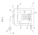
- the device for generating plasma 10 (hereinafter referred to as plasma generating device) has a chamber 104 in which plasma is generated, wherein the chamber 104 includes a gas inlet opening 110 for supplying reactant gas, a vacuum pump 112 for keeping the internal part of the chamber in a vacuum state and a gas outlet opening 114 for exhausting reactant gas after reaction.
- the chamber 104 includes a gas inlet opening 110 for supplying reactant gas, a vacuum pump 112 for keeping the internal part of the chamber in a vacuum state and a gas outlet opening 114 for exhausting reactant gas after reaction.
- a chuck 108 on which a specimen 112 like wafer, glass substrate or the like will be placed in the chamber 104.
- An antenna 100 connected with a high frequency power source 102 is installed on the chamber 104.
- An insulating plate 116 is installed between antenna 100 and chamber 104 for decreasing capacitive coupling characteristic, which helps transmission of energy from the high frequency power source 102 to plasma 118 through the inductive coupling.
- the plasma generating device 100 thus constructed generates plasma in a method which will be described below.
- all the air filling in the internal part of the chamber 104 is discharged out with a vacuum pump 112 to get to a vacuum state at the first step.
- a reactant gas is infused for generating plasma through the gas inlet opening 110, and the chamber 104 is kept at a necessary level of gas pressure.
- the high frequency power of 13.56MHz is applied to the antenna device 100 from the high frequency power source 102.
- the conventional plasma generating device 10 is constructed with a spiral shaped antenna 200 or a plurality of (for instance, three) divided electrode type antennas 202a, 202b and 202c. Therefore, with high frequency power, a vertical magnetic field is formed along with changes of time at a plane horizontal to the antenna 100.
- the magnetic field that changes in time as such forms an inductive electric field at the internal part of the chamber 104.
- electrons are heated and induced to an electric field to thereby generate plasma inductively coupled with the antenna 100.
- electrons are collided with neighboring neutral gas particles to generate ions and radicals and the like which will be used for plasma etching and deposition processes.
- power is applied to the chuck 108 from a separate high frequency power source (not shown), it is possible to adjust the energy of ions which will be applied to the specimen 106.
- a number of wires to form a spiral shaped antenna 200 are connected in series, keeping flow of current constant in each wire.
- the density of plasma is generally high, but the density of plasma decreases at a part close to the center of the chamber 104. It is also difficult to ensure the uniformity in the density distribution of plasma, and it is more difficult to treat a large size of a specimen.
- application of separately operated power results in increase in cost because an independent impedance matching circuit should be used for separate electrodes to achieve an impedance matching state for efficient uses of power.
- an antenna device for generating a large quantity of plasma comprising:
- Fig. 3a is a conceptual view for illustrating an antenna device for generating inductively coupled plasma in accordance with an embodiment of the present invention
- Fig. 4a is an equivalent circuit diagram of an antenna device shown in Fig. 3a.
- an antenna device 100 of the present invention includes a plurality of antenna units 400a and 400b connected in parallel with each other, which respectively include variable loads 302a and 302b and single or multi-wires of antennas 300a and 300b.
- reference symbols R 1 , R 2 , and L 1 , L 2 indicate resistance and equivalent inductance of respective antennas and capacitance of the antennas is absorbed and designated by reference symbols C R , C L respectively for resonance variable capacitance and variable load capacitance.
- the antenna device 100 also includes an impedance matching circuit (impedance matching box: IMB) 304 for achieving an impedance matching state between a plurality of antenna units 400a and 400b and the high frequency power source 102.
- IMB impedance matching box
- a plurality of antenna units 400a, 400b are kept in the resonant state by the variable load of the variable capacitor C R 302a, which is the most important feature of the present invention.
- the resonant state of the antenna device 100 will be described in detail in accordance with the present invention.
- Fig. 4a is an equivalent circuit diagram of the antenna device shown in Fig. 3a.
- the first antenna unit 400a includes a first variable load 302a and a first antenna 300a connected in series
- the second antenna unit 400b includes a second variable load 302b and a second antenna 300b connected in series. Both of the first and second antenna units 400a, 400b are connected in parallel.
- the magnitude of the first variable load 302a can be adjusted.
- the variable capacitor C R is used for easy adjustment of capacitance.
- a general impedance method is used for maximizing transmission of energy from the high frequency power source 102 to the first and second antenna units 400a, 400b.
- the total variable load determined at the first and second antenna units 400a, 400b can be considered as a regular load.
- an impedance matching circuit 304 for achieving an equivalent impedance matching state.
- the impedance matching circuit 304 can be constructed in a method which has been already widely known in the same technical field, for instance, in a simple circuit in which a variable inductor L I and variable capacitor C I are connected in parallel.
- the magnitude of the variable load 302b is first determined to control the level of energy transmitted by the second antenna 300b to plasma.
- the magnitude of the resonance variable load 302a is determined to form a resonant state between the first and second antennas 300a, 300b, and then an impedance matching state is achieved by the IMB 304.
- the antenna device 100' of the present invention can be constructed with a predetermined number of antenna units 410a, 410b, 410c.
- the antenna device 100' is constructed with three antenna units.
- antenna units 410a, 410b, 410c respectively includes variable loads 312a, 312b, 312c.
- the magnitude of the variable loads 312b and 312c attached in the two antenna units 410b, 410c are controlled to adjust a ratio of current flowing in the antenna units 310b, 310c.
- the rest antenna unit 310a is used for achieving a resonant state to the circuit.
- the antenna unit 310a for keeping a resonant state is formed as an outermost wire and the rest of antenna units 310b, 310c are formed as internal wires. Therefore, it is possible to conveniently improve the uniform distribution of energy in the entire antenna device.
- the variable load 312b or 312c of the internal antenna units 410b, 410c can be omitted in a particular embodiment of the present invention.
- the impedance matching state of the antenna units 410a, 410b, 410c with the high frequency power source 102' should be achieved to maximize the quantity of the energy to be supplied to the entire antenna units 410a, 410b, 410c by using the impedance matching circuit 304' having, for example, inductance L I ' and capacitance C I '.
- a large size of plasma can be conveniently formed with a uniform density distribution.
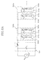
- FIG. 5 another embodiment of the present invention is presented with an additional set of antenna unit constructed in the same structure as those of 400a and 400b of the antenna device 100 shown in Fig. 3.
- the equivalent circuit diagram of the antenna device 500 shown in Fig. 6 includes a first set of antenna units 520a having first and second antenna units 510a, 510b and a second set of antenna units 520b having third and fourth antenna units 510c, 510d.
- Variable loads as in the other embodiment of the present invention, can be imposed onto all of the antenna units 510a, 510b, 510c, 510d.
- the resonant state is kept between the antenna units 510a and 510b, 510c and 510d of the respective sets of antenna units 520a, 520b by adjusting the magnitude of the resonance variable load C R1 or C R2 . Furthermore, transmission of energy is maximized by using the impedance matching circuit 504 connected between the entire sets of antenna units 520a, 520b and the high frequency power source 102'.
- the number of antenna sets can be controlled for increasing the size of plasma and adjusting uniformity in the density distribution of plasma more precisely.
- a resonant state may not be established in the set of antenna units 520b positioned inside.
- the uniformity in the density distribution of plasma can be improved by supplying a lower level of power to plasma from the antenna set 520b than that from the antenna set 520a positioned outside.
- the greater quantity of power can be also supplied by keeping the set of external antenna units 520a at a resonant state.
- Fig. 6b illustrates an antenna device 600 having two or more sets of antenna units, wherein the sets of antenna units respectively include three antenna units. As shown in Fig. 6b, all the descriptions on the level of energy to be supplied to each antenna unit and formation of an impedance matching state with the high frequency power source are the same or similar to the aforementioned embodiments of the present invention.
- the antenna device for generating inductively coupled plasma in that an impedance mismatching state does not result from an increase in the size of the antenna device, and uniformity in the density distribution of plasma is achieved by inducing a resonant state into the antenna device through selective adjustment of the level of the energy to be transmitted through particular antennas.
Landscapes
- Physics & Mathematics (AREA)
- Engineering & Computer Science (AREA)
- Plasma & Fusion (AREA)
- Electromagnetism (AREA)
- Spectroscopy & Molecular Physics (AREA)
- Chemical & Material Sciences (AREA)
- Analytical Chemistry (AREA)
- Plasma Technology (AREA)
- Drying Of Semiconductors (AREA)
- Chemical Vapour Deposition (AREA)
Abstract
Description
Claims (12)
- An antenna device for generating a large quantity of plasma comprising:a high frequency power source;a first antenna for receiving the high frequency power supplied from the high frequency power source; anda second antenna connected in parallel with the first antenna for receiving the high frequency power supplied from the high frequency power source, wherein a resonant state is kept between the first and second antennas.
- The device, as defined in claim 1, wherein the second antenna is connected with a variable load for keeping a resonant state with the first antenna.
- The device, as defined in claim 1, wherein a third antenna is additionally connected in parallel with the first and second antennas.
- The device, as defined in claim 3, wherein a resonant state is kept among the first, second and third antennas.
- The device, as defined in claim 1 or 4, wherein an impedance matching circuit is additionally assembled for achieving an impedance matching state between the high frequency power source and the first and second antennas.
- An antenna device for generating a large quantity of plasma comprising:wherein a resonant state is kept between the first and second antennas.a high frequency power source;a first antenna set having first and second antennas connected in parallel for receiving the high frequency power supplied from the high frequency power source; anda second antenna set having third and fourth antennas connected in parallel for receiving the high frequency power supplied from the high frequency power source and being connected in parallel with the first antenna set
- The device, as defined in claim 6, wherein the second antenna is connected with a variable load for keeping a resonant state with the first antenna.
- The device, as defined in claim 6, wherein a resonant state is kept among the third, fourth antennas.
- The device, as defined in claim 8, wherein the fourth antenna is connected with a variable load for keeping a resonant state with the third antenna.
- The device, as defined in claim 6, wherein a fifth antenna is additionally connected in parallel with the first and second antennas.
- The device, as defined in claim 6 or 10, wherein an impedance matching circuit is additionally assembled for achieving an impedance matching state between the high frequency power source and the first and second antenna sets.
- The device, as defined in claim 6 or 10, wherein a resonant state is kept between the first and second antenna sets.
Applications Claiming Priority (2)
| Application Number | Priority Date | Filing Date | Title |
|---|---|---|---|
| KR9935702 | 1999-08-26 | ||
| KR1019990035702A KR100338057B1 (en) | 1999-08-26 | 1999-08-26 | Antenna device for generating inductively coupled plasma |
Publications (2)
| Publication Number | Publication Date |
|---|---|
| EP1079671A2 true EP1079671A2 (en) | 2001-02-28 |
| EP1079671A3 EP1079671A3 (en) | 2001-11-07 |
Family
ID=19608827
Family Applications (1)
| Application Number | Title | Priority Date | Filing Date |
|---|---|---|---|
| EP00401460A Withdrawn EP1079671A3 (en) | 1999-08-26 | 2000-05-25 | Antenna device for generating inductively coupled plasma |
Country Status (5)
| Country | Link |
|---|---|
| US (1) | US6288493B1 (en) |
| EP (1) | EP1079671A3 (en) |
| JP (1) | JP2001085196A (en) |
| KR (1) | KR100338057B1 (en) |
| TW (1) | TW447226B (en) |
Cited By (6)
| Publication number | Priority date | Publication date | Assignee | Title |
|---|---|---|---|---|
| WO2004001822A1 (en) * | 2002-06-19 | 2003-12-31 | Mitsubishi Heavy Industries, Ltd. | Plasma processing system, plasma processing method, plasma film deposition system, and plasma film deposition method |
| WO2004012483A1 (en) * | 2002-07-26 | 2004-02-05 | Plasmart Co. Ltd. | Inductively coupled plasma generator having lower aspect ratio |
| WO2003087857A3 (en) * | 2002-04-18 | 2004-02-26 | Ackermann Patent Gmbh | Method and device for picking-up and processing interference fields and interference beams |
| US7079085B2 (en) | 2001-07-30 | 2006-07-18 | Plasmart Co. Ltd. | Antenna structure for inductively coupled plasma generator |
| EP1637624A4 (en) * | 2003-06-02 | 2007-12-26 | Shincron Co Ltd | THIN FILM FORMING DEVICE AND THIN FILM FORMING METHOD |
| WO2010092433A1 (en) * | 2009-02-10 | 2010-08-19 | HELYSSEN Sàrl | Apparatus for large area plasma processing |
Families Citing this family (87)
| Publication number | Priority date | Publication date | Assignee | Title |
|---|---|---|---|---|
| US6744213B2 (en) * | 1999-11-15 | 2004-06-01 | Lam Research Corporation | Antenna for producing uniform process rates |
| JP2002008996A (en) * | 2000-06-23 | 2002-01-11 | Mitsubishi Heavy Ind Ltd | Feeding antenna and feeding method |
| JP4598267B2 (en) | 2000-12-26 | 2010-12-15 | レノボ シンガポール プライヴェート リミテッド | Transmission device, computer system, and opening / closing structure |
| KR100440736B1 (en) * | 2001-02-19 | 2004-07-15 | 오범환 | Direct Inductance Controller for Coaxial Parallel ICP Antenna |
| US7096819B2 (en) * | 2001-03-30 | 2006-08-29 | Lam Research Corporation | Inductive plasma processor having coil with plural windings and method of controlling plasma density |
| KR100773204B1 (en) * | 2001-04-13 | 2007-11-02 | 어플라이드 머티어리얼스, 인코포레이티드 | Inductively Coupled Plasma Sources That Control Power Distribution |
| KR100404723B1 (en) * | 2001-04-26 | 2003-11-07 | 주식회사 플라즈마트 | Device for Generating Inductively Coupled Plasma with Lower Aspect Ratio |
| KR100396214B1 (en) * | 2001-06-19 | 2003-09-02 | 주성엔지니어링(주) | Plasma processing apparatus having parallel resonance antenna for very high frequency |
| KR100476902B1 (en) * | 2001-07-20 | 2005-03-17 | 주식회사 셈테크놀러지 | The Large-Area Plasma Antenna(LAPA) and The Plasma Source For Making Uniform Plasma |
| KR100464808B1 (en) * | 2001-08-28 | 2005-01-05 | 최대규 | Multi inductively coupled plasma inductor |
| KR100428813B1 (en) * | 2001-09-18 | 2004-04-29 | 주성엔지니어링(주) | Plama generation apparatus and SiO2 thin film etching method using the same |
| KR100415944B1 (en) * | 2001-10-09 | 2004-01-24 | 주성엔지니어링(주) | inductive coupled plasma generation source |
| KR100420533B1 (en) * | 2001-12-05 | 2004-03-02 | 주성엔지니어링(주) | Plasma apparatus and plasma etching method using the same |
| KR100478106B1 (en) * | 2001-12-10 | 2005-03-24 | (주)울텍 | Apparatus of high density plasma |
| KR100488362B1 (en) * | 2002-05-20 | 2005-05-11 | 주식회사 플라즈마트 | Low-Frequency Type Inductively Coupled Plasma Generating Device |
| KR100488360B1 (en) * | 2002-07-29 | 2005-05-11 | 주식회사 플라즈마트 | Antenna Structure of Inductively Coupled Plasma Generating Device for Flat Displayer |
| US20030015965A1 (en) * | 2002-08-15 | 2003-01-23 | Valery Godyak | Inductively coupled plasma reactor |
| KR100486724B1 (en) * | 2002-10-15 | 2005-05-03 | 삼성전자주식회사 | Inductively coupled plasma generating apparatus with serpentine coil antenna |
| KR100964398B1 (en) * | 2003-01-03 | 2010-06-17 | 삼성전자주식회사 | Inductively Coupled Antenna and Plasma Processing Equipment Employing the Same |
| JP3783689B2 (en) * | 2003-02-28 | 2006-06-07 | ソニー株式会社 | Antenna device |
| US7871490B2 (en) * | 2003-03-18 | 2011-01-18 | Top Engineering Co., Ltd. | Inductively coupled plasma generation system with a parallel antenna array having evenly distributed power input and ground nodes and improved field distribution |
| US20040182319A1 (en) * | 2003-03-18 | 2004-09-23 | Harqkyun Kim | Inductively coupled plasma generation system with a parallel antenna array having evenly distributed power input and ground nodes |
| KR100523851B1 (en) | 2003-05-07 | 2005-10-27 | 학교법인 성균관대학 | Inductively Coupled Plasma Processing Appratus having internal linear antenna for large area processing |
| US8974630B2 (en) | 2003-05-07 | 2015-03-10 | Sungkyunkwan University | Inductively coupled plasma processing apparatus having internal linear antenna for large area processing |
| KR101038204B1 (en) * | 2004-02-25 | 2011-05-31 | 주성엔지니어링(주) | Plasma Generating Antenna |
| US7253125B1 (en) | 2004-04-16 | 2007-08-07 | Novellus Systems, Inc. | Method to improve mechanical strength of low-k dielectric film using modulated UV exposure |
| JP4344886B2 (en) * | 2004-09-06 | 2009-10-14 | 東京エレクトロン株式会社 | Plasma processing equipment |
| US9659769B1 (en) | 2004-10-22 | 2017-05-23 | Novellus Systems, Inc. | Tensile dielectric films using UV curing |
| US8980769B1 (en) | 2005-04-26 | 2015-03-17 | Novellus Systems, Inc. | Multi-station sequential curing of dielectric films |
| US8282768B1 (en) | 2005-04-26 | 2012-10-09 | Novellus Systems, Inc. | Purging of porogen from UV cure chamber |
| US8137465B1 (en) | 2005-04-26 | 2012-03-20 | Novellus Systems, Inc. | Single-chamber sequential curing of semiconductor wafers |
| US8454750B1 (en) * | 2005-04-26 | 2013-06-04 | Novellus Systems, Inc. | Multi-station sequential curing of dielectric films |
| US8889233B1 (en) | 2005-04-26 | 2014-11-18 | Novellus Systems, Inc. | Method for reducing stress in porous dielectric films |
| US20060257342A1 (en) * | 2005-05-12 | 2006-11-16 | Weilin Mu | Long-wearing glossy cosmetic composition |
| US8398816B1 (en) | 2006-03-28 | 2013-03-19 | Novellus Systems, Inc. | Method and apparatuses for reducing porogen accumulation from a UV-cure chamber |
| JP2007311182A (en) * | 2006-05-18 | 2007-11-29 | Tokyo Electron Ltd | Inductively coupled plasma processing apparatus and plasma processing method |
| KR100824974B1 (en) * | 2006-08-17 | 2008-04-28 | (주)아이씨디 | Plasma Processing Antenna |
| CN101136279B (en) * | 2006-08-28 | 2010-05-12 | 北京北方微电子基地设备工艺研究中心有限责任公司 | Jigger coupling coil and jigger coupling plasma device |
| US10037905B2 (en) | 2009-11-12 | 2018-07-31 | Novellus Systems, Inc. | UV and reducing treatment for K recovery and surface clean in semiconductor processing |
| US9050623B1 (en) | 2008-09-12 | 2015-06-09 | Novellus Systems, Inc. | Progressive UV cure |
| JP5399151B2 (en) * | 2008-10-27 | 2014-01-29 | 東京エレクトロン株式会社 | Inductively coupled plasma processing apparatus, plasma processing method, and storage medium |
| US8319436B2 (en) * | 2009-02-02 | 2012-11-27 | Advanced Energy Industries, Inc. | Passive power distribution for multiple electrode inductive plasma source |
| US9305750B2 (en) * | 2009-06-12 | 2016-04-05 | Lam Research Corporation | Adjusting current ratios in inductively coupled plasma processing systems |
| KR101757922B1 (en) | 2009-10-27 | 2017-07-14 | 도쿄엘렉트론가부시키가이샤 | Plamsa processing apparatus |
| US9313872B2 (en) | 2009-10-27 | 2016-04-12 | Tokyo Electron Limited | Plasma processing apparatus and plasma processing method |
| JP5554047B2 (en) * | 2009-10-27 | 2014-07-23 | 東京エレクトロン株式会社 | Plasma processing equipment |
| JP5592098B2 (en) | 2009-10-27 | 2014-09-17 | 東京エレクトロン株式会社 | Plasma processing apparatus and plasma processing method |
| US9967965B2 (en) * | 2010-08-06 | 2018-05-08 | Lam Research Corporation | Distributed, concentric multi-zone plasma source systems, methods and apparatus |
| JP5723130B2 (en) * | 2010-09-28 | 2015-05-27 | 東京エレクトロン株式会社 | Plasma processing equipment |
| JP5916044B2 (en) | 2010-09-28 | 2016-05-11 | 東京エレクトロン株式会社 | Plasma processing apparatus and plasma processing method |
| JP5851682B2 (en) | 2010-09-28 | 2016-02-03 | 東京エレクトロン株式会社 | Plasma processing equipment |
| KR20120035559A (en) * | 2010-10-06 | 2012-04-16 | 주식회사 유진테크 | Substrate processing apparatus including semicircle-type antenna |
| KR101246809B1 (en) * | 2010-12-21 | 2013-03-26 | 엘아이지에이디피 주식회사 | Apparatus for plasma processing and antenna thereof |
| JP5800532B2 (en) * | 2011-03-03 | 2015-10-28 | 東京エレクトロン株式会社 | Plasma processing apparatus and plasma processing method |
| JP5800547B2 (en) * | 2011-03-29 | 2015-10-28 | 東京エレクトロン株式会社 | Plasma processing apparatus and plasma processing method |
| KR101853370B1 (en) * | 2011-09-16 | 2018-04-30 | 세메스 주식회사 | Antenna structure and plasma generating device |
| JP5878771B2 (en) * | 2012-02-07 | 2016-03-08 | 東京エレクトロン株式会社 | Inductively coupled plasma processing method and inductively coupled plasma processing apparatus |
| US20130256271A1 (en) * | 2012-04-03 | 2013-10-03 | Theodoros Panagopoulos | Methods and apparatuses for controlling plasma in a plasma processing chamber |
| US9685297B2 (en) | 2012-08-28 | 2017-06-20 | Advanced Energy Industries, Inc. | Systems and methods for monitoring faults, anomalies, and other characteristics of a switched mode ion energy distribution system |
| US9082589B2 (en) * | 2012-10-09 | 2015-07-14 | Novellus Systems, Inc. | Hybrid impedance matching for inductively coupled plasma system |
| KR101468656B1 (en) * | 2012-12-28 | 2014-12-04 | 엘아이지에이디피 주식회사 | Inductively coupled plasma processing apparatus |
| KR101619896B1 (en) * | 2014-07-25 | 2016-05-23 | 인베니아 주식회사 | An plasma process apparatus and an antenna assembly for that |
| US10332725B2 (en) * | 2015-03-30 | 2019-06-25 | Lam Research Corporation | Systems and methods for reversing RF current polarity at one output of a multiple output RF matching network |
| US10388546B2 (en) | 2015-11-16 | 2019-08-20 | Lam Research Corporation | Apparatus for UV flowable dielectric |
| CN107333378B (en) * | 2016-04-29 | 2019-05-03 | 中微半导体设备(上海)股份有限公司 | A kind of device for inductively coupled plasma processing and its control method |
| US10347547B2 (en) | 2016-08-09 | 2019-07-09 | Lam Research Corporation | Suppressing interfacial reactions by varying the wafer temperature throughout deposition |
| US9847221B1 (en) | 2016-09-29 | 2017-12-19 | Lam Research Corporation | Low temperature formation of high quality silicon oxide films in semiconductor device manufacturing |
| US11651939B2 (en) | 2017-07-07 | 2023-05-16 | Advanced Energy Industries, Inc. | Inter-period control system for plasma power delivery system and method of operating same |
| US11615943B2 (en) | 2017-07-07 | 2023-03-28 | Advanced Energy Industries, Inc. | Inter-period control for passive power distribution of multiple electrode inductive plasma source |
| KR101972783B1 (en) * | 2017-10-13 | 2019-08-16 | 주식회사 유진테크 | Icp antenna and plasma processing apparatus including the same |
| US12230476B2 (en) | 2017-11-17 | 2025-02-18 | Advanced Energy Industries, Inc. | Integrated control of a plasma processing system |
| US11437221B2 (en) | 2017-11-17 | 2022-09-06 | Advanced Energy Industries, Inc. | Spatial monitoring and control of plasma processing environments |
| US12505986B2 (en) | 2017-11-17 | 2025-12-23 | Advanced Energy Industries, Inc. | Synchronization of plasma processing components |
| TWI872423B (en) | 2017-11-17 | 2025-02-11 | 新加坡商Aes 全球公司 | Systems and methods for spatially and temporally controlling plasma processing on substrates and related computer-readable medium |
| KR102791775B1 (en) | 2019-05-07 | 2025-04-03 | 램 리써치 코포레이션 | Closed-loop multiple output radio frequency (rf) matching |
| JP7352068B2 (en) * | 2019-07-12 | 2023-09-28 | 日新電機株式会社 | plasma control system |
| KR102882813B1 (en) | 2019-07-31 | 2025-11-06 | 램 리써치 코포레이션 | Radio frequency (RF) power generator with multiple output ports |
| KR20260010468A (en) | 2019-12-02 | 2026-01-20 | 램 리써치 코포레이션 | Impedance transformation in radio-frequency-assisted plasma generation |
| US11994542B2 (en) | 2020-03-27 | 2024-05-28 | Lam Research Corporation | RF signal parameter measurement in an integrated circuit fabrication chamber |
| US12626895B2 (en) | 2020-03-27 | 2026-05-12 | Lam Research Corporation | RF signal parameter measurement in an integrated circuit fabrication chamber |
| CN116075917A (en) | 2020-06-12 | 2023-05-05 | 朗姆研究公司 | Control of Plasma Formation by RF Coupling Structures |
| US11942309B2 (en) | 2022-01-26 | 2024-03-26 | Advanced Energy Industries, Inc. | Bias supply with resonant switching |
| US11670487B1 (en) | 2022-01-26 | 2023-06-06 | Advanced Energy Industries, Inc. | Bias supply control and data processing |
| US12046448B2 (en) | 2022-01-26 | 2024-07-23 | Advanced Energy Industries, Inc. | Active switch on time control for bias supply |
| US11978613B2 (en) | 2022-09-01 | 2024-05-07 | Advanced Energy Industries, Inc. | Transition control in a bias supply |
| US12567572B2 (en) | 2023-07-11 | 2026-03-03 | Advanced Energy Industries, Inc. | Plasma behaviors predicted by current measurements during asymmetric bias waveform application |
| CN121282077A (en) * | 2025-09-30 | 2026-01-06 | 苏州苏纳光电有限公司 | Semiconductor processing control method and related device |
Family Cites Families (21)
| Publication number | Priority date | Publication date | Assignee | Title |
|---|---|---|---|---|
| US6068784A (en) * | 1989-10-03 | 2000-05-30 | Applied Materials, Inc. | Process used in an RF coupled plasma reactor |
| US6165311A (en) * | 1991-06-27 | 2000-12-26 | Applied Materials, Inc. | Inductively coupled RF plasma reactor having an overhead solenoidal antenna |
| JPH06104184A (en) * | 1992-09-18 | 1994-04-15 | Fujitsu Ltd | Plasma processing device |
| US5401350A (en) * | 1993-03-08 | 1995-03-28 | Lsi Logic Corporation | Coil configurations for improved uniformity in inductively coupled plasma systems |
| US5587038A (en) * | 1994-06-16 | 1996-12-24 | Princeton University | Apparatus and process for producing high density axially extending plasmas |
| US5540824A (en) * | 1994-07-18 | 1996-07-30 | Applied Materials | Plasma reactor with multi-section RF coil and isolated conducting lid |
| US5919382A (en) * | 1994-10-31 | 1999-07-06 | Applied Materials, Inc. | Automatic frequency tuning of an RF power source of an inductively coupled plasma reactor |
| JPH08279493A (en) * | 1995-04-04 | 1996-10-22 | Anelva Corp | Plasma processing device |
| US6034346A (en) * | 1995-05-19 | 2000-03-07 | Hitachi, Ltd. | Method and apparatus for plasma processing apparatus |
| US5874704A (en) * | 1995-06-30 | 1999-02-23 | Lam Research Corporation | Low inductance large area coil for an inductively coupled plasma source |
| JP3153743B2 (en) * | 1995-08-31 | 2001-04-09 | 東京エレクトロン株式会社 | Plasma processing equipment |
| KR100290813B1 (en) * | 1995-08-17 | 2001-06-01 | 히가시 데쓰로 | Plasma processing equipment |
| JPH09102471A (en) * | 1995-10-05 | 1997-04-15 | Sony Corp | Plasma generation source, plasma CVD apparatus and plasma CVD method |
| US5965034A (en) * | 1995-12-04 | 1999-10-12 | Mc Electronics Co., Ltd. | High frequency plasma process wherein the plasma is executed by an inductive structure in which the phase and anti-phase portion of the capacitive currents between the inductive structure and the plasma are balanced |
| US6017221A (en) * | 1995-12-04 | 2000-01-25 | Flamm; Daniel L. | Process depending on plasma discharges sustained by inductive coupling |
| US5767628A (en) * | 1995-12-20 | 1998-06-16 | International Business Machines Corporation | Helicon plasma processing tool utilizing a ferromagnetic induction coil with an internal cooling channel |
| JP3739137B2 (en) * | 1996-06-18 | 2006-01-25 | 日本電気株式会社 | Plasma generator and surface treatment apparatus using the plasma generator |
| JPH10134996A (en) * | 1996-10-31 | 1998-05-22 | Nec Corp | Plasma treatment equipment |
| JPH11144894A (en) * | 1997-08-29 | 1999-05-28 | Matsushita Electric Ind Co Ltd | Plasma processing method and apparatus |
| JPH11185993A (en) * | 1997-12-24 | 1999-07-09 | Matsushita Electric Ind Co Ltd | Plasma processing method and apparatus |
| US6164241A (en) * | 1998-06-30 | 2000-12-26 | Lam Research Corporation | Multiple coil antenna for inductively-coupled plasma generation systems |
-
1999
- 1999-08-26 KR KR1019990035702A patent/KR100338057B1/en not_active Expired - Fee Related
-
2000
- 2000-05-02 US US09/562,902 patent/US6288493B1/en not_active Expired - Lifetime
- 2000-05-09 TW TW089108834A patent/TW447226B/en not_active IP Right Cessation
- 2000-05-25 EP EP00401460A patent/EP1079671A3/en not_active Withdrawn
- 2000-06-27 JP JP2000192572A patent/JP2001085196A/en active Pending
Cited By (11)
| Publication number | Priority date | Publication date | Assignee | Title |
|---|---|---|---|---|
| US7079085B2 (en) | 2001-07-30 | 2006-07-18 | Plasmart Co. Ltd. | Antenna structure for inductively coupled plasma generator |
| WO2003087857A3 (en) * | 2002-04-18 | 2004-02-26 | Ackermann Patent Gmbh | Method and device for picking-up and processing interference fields and interference beams |
| WO2004001822A1 (en) * | 2002-06-19 | 2003-12-31 | Mitsubishi Heavy Industries, Ltd. | Plasma processing system, plasma processing method, plasma film deposition system, and plasma film deposition method |
| US8662010B2 (en) | 2002-06-19 | 2014-03-04 | Mitsubishi Heavy Industries, Ltd. | Plasma processing apparatus, plasma processing method, plasma film deposition apparatus, and plasma film deposition method |
| WO2004012483A1 (en) * | 2002-07-26 | 2004-02-05 | Plasmart Co. Ltd. | Inductively coupled plasma generator having lower aspect ratio |
| US7088047B2 (en) | 2002-07-26 | 2006-08-08 | Plasmart Co. Ltd. | Inductively coupled plasma generator having low aspect ratio |
| CN1298198C (en) * | 2002-07-26 | 2007-01-31 | 株式会社普来马特 | Inductively coupled plasma generator having lower aspect ratio |
| EP1637624A4 (en) * | 2003-06-02 | 2007-12-26 | Shincron Co Ltd | THIN FILM FORMING DEVICE AND THIN FILM FORMING METHOD |
| WO2010092433A1 (en) * | 2009-02-10 | 2010-08-19 | HELYSSEN Sàrl | Apparatus for large area plasma processing |
| RU2507628C2 (en) * | 2009-02-10 | 2014-02-20 | ЭЛИССЕН Сарл | Apparatus for plasma treatment of large areas |
| US10242843B2 (en) | 2009-02-10 | 2019-03-26 | HELYSSEN Sàrl | Apparatus for large area plasma processing |
Also Published As
| Publication number | Publication date |
|---|---|
| KR100338057B1 (en) | 2002-05-24 |
| US6288493B1 (en) | 2001-09-11 |
| EP1079671A3 (en) | 2001-11-07 |
| TW447226B (en) | 2001-07-21 |
| JP2001085196A (en) | 2001-03-30 |
| KR20000053680A (en) | 2000-09-05 |
Similar Documents
| Publication | Publication Date | Title |
|---|---|---|
| US6288493B1 (en) | Antenna device for generating inductively coupled plasma | |
| US7079085B2 (en) | Antenna structure for inductively coupled plasma generator | |
| US7442273B2 (en) | Apparatus using hybrid coupled plasma | |
| EP0413282B1 (en) | Method and apparatus for producing magnetically-coupled planar plasma | |
| US6451161B1 (en) | Method and apparatus for generating high-density uniform plasma | |
| US20100101727A1 (en) | Capacitively coupled remote plasma source with large operating pressure range | |
| WO2000000993A1 (en) | Multiple coil antenna for inductively-coupled plasma generation systems | |
| US20020007794A1 (en) | Plasma processing apparatus | |
| KR20070033222A (en) | Plasma Generating Antenna | |
| KR101572100B1 (en) | Large area plasma reactor using complex frequency | |
| KR100488363B1 (en) | Antenna Structure of Inductively Coupled Plasma Generating Device | |
| US7088047B2 (en) | Inductively coupled plasma generator having low aspect ratio | |
| KR100845890B1 (en) | Large Area Inductively Coupled Plasma Reactor | |
| KR100864111B1 (en) | Inductively coupled plasma reactor | |
| KR100391063B1 (en) | Device and Method for Generating Capacitively Coupled Plasma Enhanced Inductively Coupled Plasma | |
| KR101236206B1 (en) | Inductively coupled plasma reactor for generating high density uniform plasma | |
| KR100786537B1 (en) | Multiple Plasma Generation Sources Used in Semiconductor Substrate Process Chambers | |
| KR20050049169A (en) | System for generating inductively coupled plasma and antenna coil structure for generating inductive electric field | |
| KR100404723B1 (en) | Device for Generating Inductively Coupled Plasma with Lower Aspect Ratio | |
| CN107305830A (en) | Capacitance coupling plasma processing unit and method of plasma processing | |
| KR101040541B1 (en) | Hybrid antenna for plasma generation | |
| KR100753869B1 (en) | Hybrid Plasma Reactor | |
| KR100364636B1 (en) | Device for Generating Inductively Coupled Plasma which Power Supplied by Mutual Induction | |
| KR100488362B1 (en) | Low-Frequency Type Inductively Coupled Plasma Generating Device |
Legal Events
| Date | Code | Title | Description |
|---|---|---|---|
| PUAI | Public reference made under article 153(3) epc to a published international application that has entered the european phase |
Free format text: ORIGINAL CODE: 0009012 |
|
| 17P | Request for examination filed |
Effective date: 20000619 |
|
| AK | Designated contracting states |
Kind code of ref document: A2 Designated state(s): AT BE CH CY DE DK ES FI FR GB GR IE IT LI LU MC NL PT SE Kind code of ref document: A2 Designated state(s): DE FR GB |
|
| AX | Request for extension of the european patent |
Free format text: AL;LT;LV;MK;RO;SI |
|
| PUAL | Search report despatched |
Free format text: ORIGINAL CODE: 0009013 |
|
| AK | Designated contracting states |
Kind code of ref document: A3 Designated state(s): AT BE CH CY DE DK ES FI FR GB GR IE IT LI LU MC NL PT SE |
|
| AX | Request for extension of the european patent |
Free format text: AL;LT;LV;MK;RO;SI |
|
| AKX | Designation fees paid |
Free format text: DE FR GB |
|
| RAP1 | Party data changed (applicant data changed or rights of an application transferred) |
Owner name: JUSUNG ENGINEERING CO. LTD. |
|
| 17Q | First examination report despatched |
Effective date: 20070502 |
|
| GRAP | Despatch of communication of intention to grant a patent |
Free format text: ORIGINAL CODE: EPIDOSNIGR1 |
|
| STAA | Information on the status of an ep patent application or granted ep patent |
Free format text: STATUS: THE APPLICATION IS DEEMED TO BE WITHDRAWN |
|
| 18D | Application deemed to be withdrawn |
Effective date: 20091124 |