EP1079531A2 - Integrierte Halbleiterschaltung zur Bearbeitung von Empfangssignalen - Google Patents
Integrierte Halbleiterschaltung zur Bearbeitung von Empfangssignalen Download PDFInfo
- Publication number
- EP1079531A2 EP1079531A2 EP00115061A EP00115061A EP1079531A2 EP 1079531 A2 EP1079531 A2 EP 1079531A2 EP 00115061 A EP00115061 A EP 00115061A EP 00115061 A EP00115061 A EP 00115061A EP 1079531 A2 EP1079531 A2 EP 1079531A2
- Authority
- EP
- European Patent Office
- Prior art keywords
- signal
- frequency
- band
- circuit
- frequency band
- Prior art date
- Legal status (The legal status is an assumption and is not a legal conclusion. Google has not performed a legal analysis and makes no representation as to the accuracy of the status listed.)
- Withdrawn
Links
Images


Classifications
-
- H—ELECTRICITY
- H04—ELECTRIC COMMUNICATION TECHNIQUE
- H04B—TRANSMISSION
- H04B1/00—Details of transmission systems, not covered by a single one of groups H04B3/00 - H04B13/00; Details of transmission systems not characterised by the medium used for transmission
- H04B1/06—Receivers
- H04B1/16—Circuits
- H04B1/26—Circuits for superheterodyne receivers
- H04B1/28—Circuits for superheterodyne receivers the receiver comprising at least one semiconductor device having three or more electrodes
-
- H—ELECTRICITY
- H04—ELECTRIC COMMUNICATION TECHNIQUE
- H04B—TRANSMISSION
- H04B1/00—Details of transmission systems, not covered by a single one of groups H04B3/00 - H04B13/00; Details of transmission systems not characterised by the medium used for transmission
- H04B1/005—Details of transmission systems, not covered by a single one of groups H04B3/00 - H04B13/00; Details of transmission systems not characterised by the medium used for transmission adapting radio receivers, transmitters andtransceivers for operation on two or more bands, i.e. frequency ranges
- H04B1/0053—Details of transmission systems, not covered by a single one of groups H04B3/00 - H04B13/00; Details of transmission systems not characterised by the medium used for transmission adapting radio receivers, transmitters andtransceivers for operation on two or more bands, i.e. frequency ranges with common antenna for more than one band
- H04B1/0057—Details of transmission systems, not covered by a single one of groups H04B3/00 - H04B13/00; Details of transmission systems not characterised by the medium used for transmission adapting radio receivers, transmitters andtransceivers for operation on two or more bands, i.e. frequency ranges with common antenna for more than one band using diplexing or multiplexing filters for selecting the desired band
-
- H—ELECTRICITY
- H04—ELECTRIC COMMUNICATION TECHNIQUE
- H04B—TRANSMISSION
- H04B1/00—Details of transmission systems, not covered by a single one of groups H04B3/00 - H04B13/00; Details of transmission systems not characterised by the medium used for transmission
- H04B1/06—Receivers
- H04B1/16—Circuits
- H04B1/30—Circuits for homodyne or synchrodyne receivers
Definitions
- the present invention relates to a wireless communications technology particularly to a useful technique for receiving and processing signals in a plurality of frequency bands; said technique is usefully applied to, for example, an integrated semiconductor circuit for receiving signal processing in a terminal equipment which composes a part of DAB (Digital Audio Broadcasting) system that handles two frequency bands, L-band and VHF-band.
- DAB Digital Audio Broadcasting
- a DAB system uses two frequency bands, one 1,452 - 1,492 MHz in L-band and the other 174 - 245 MHz in VHF-band. Therefore, terminal equipment like portable telephones and personal computers are required to have a circuit capable of processing or handling signals in two frequency bands.
- said circuit is provided separately for each frequency band using a semiconductor integrated circuit therein, number of parts in said terminal equipment increases. Particularly in a handheld electronic device like a portable telephone, small sizing and power consumption lowering are vital and reducing number of parts is an important technical object.
- the inventors of the present invention studied a signal processing technique that permits amplification and noise elimination on one common circuit by converting the signal in one frequency band into the signal in the other frequency band.
- a signal processing technique that permits amplification and noise elimination on one common circuit by converting the signal in one frequency band into the signal in the other frequency band.
- reference numeral 101 indicates a deplexer (branching filter) which separately extracts L-band signals of 1,452 - 1,492 MHz and VHF-band signals of 174 - 245 MHz form the received signal received by an antenna 100;
- reference numeral 102 indicates a signal switcher;
- reference numerals 111, 112, and 114 indicate low-noise amplifiers (LNAs);
- reference numeral 113 indicates an automatic gain control (AGC) amplifier;
- reference numerals 121, 122, 123, 124 and 125 indicate band-pass filters;
- reference numerals 131, 132 and 133 indicate PLL (phase locked loop) circuits which generate pre-determined frequencies as local oscillators; and
- reference numerals 141, 142 and 143 indicate mixers which combine said received signal and oscillating signals generated from said PLL circuits.
- circuitry is devised by the inventors for study purpose and is not meant a public known circuitry.
- said PLL circuit 131 is composed to generate a local oscillating signal of 1,269.992 MHz; the receiving L-band signal of 1,452 - 1,492 MHz received by said antenna 100 and separately extracted by said deplexer (branching filter) 101 is amplified by said low-noise amplifier 111, and is processed by said band-pass filter 121 for noise elimination, then further is down-converted into the signal on a frequency close to VHF-band by the combining process in a first mixer 141 with said local oscillating signal of 1,269.992 MHz generated from said PLL circuit 131.
- Said mixers 141 - 143 send out a superposed signal which is an overlay of two frequencies: one equivalent to the sum-frequency of frequencies of said receiving signal and said oscillating signal, the other equivalent to the differential-frequency between said frequencies.
- Said receiving L-band signal down-converted by a first mixer 141 is fed to said signal switcher 102 via said band-pass filter 122 in a form of the signal on frequencies of 182.008 - 222.008 MHz equivalent to the differential-frequency between frequencies of said receiving signal and said local oscillating signal.
- Said signal switcher 102 selectively sends out either said down-converted L-band signal or said VHF-band signal to said low-noise amplifier 112 according to selected mode.
- the signal amplified by said low-noise amplifier 112 is processed for noise elimination therefrom by said band-pass filter 123, and is converted into an intermediate frequency signal (IF signal) of 38.9 MHz by a second mixer 142 by being combined with a local oscillating signal of 212.9 - 283.9 MHz generated from said PLL circuit 132 for converting.
- IF signal intermediate frequency signal
- Said converted signal after being processed for noise elimination therefrom by a narrow-band band-pass filter 124 like a SAW filter, is amplified by said automatic gain control (ACG) amplifier 113 followed by a frequency conversion into a signal on 2 MHz in a third mixer 143 by combining with a local oscillating signal of 40.9 MHz generated from said PLL circuit 133, then is sent out to a demodulating circuit through said band-pass filter 125 and said amplifier 114.
- ACG automatic gain control
- said noise fu-fw has a very close frequency to a signal frequency of 1stIF 38.912 MHz a converted frequency from said signal fw on 180 MHz channel to be selected; this causes a problem that the noise cannot be eliminated, as can be understood from Figure 8(d), even by a SAW filter 124, a narrow-band band-pass filter, placed at the front-end thereof.
- signs e, f, h and i appear in upper-right corners of Figure signs (a) - (d) for identification show corresponding signals among signals marked as a - i in the system given in Figure 7.
- FIG. 9 shows a signal frequency distribution at each part of the circuit when a tracking filter is used as said band-pass filter 123.
- a tracking filter as said band-pass filter 123 can obtain a signal without said noise fu-fw of 38.928 MHz by shifting its pass-band to the vicinity of 180 MHz channel to be selected as shown in Figure 9(b) to eliminate said signal fu of 218.928 MHz in undesired other channel.
- This technique still has a problem that number of parts therein becomes increased, because, the tracking filter to be used here should have a sophisticated circuitry containing variable capacitance diodes and many other parts.
- the oscillating frequency in said PLL circuit 132 which generates a local oscillating signal to be combined with said received signal in said second mixer 142, must be capable of being varied by about 30% of the center frequency of said desired channel in a wide range from 212.9 - 283.9 MHz.
- VCO voltage controlled oscillator
- the semiconductor integrated circuit to be used in a handheld electronic device like a portable telephone is required to operate with a low, as much as possible, voltage battery consuming less electrical power. Therefore, it has been revealed that said down-converting technique was unsuitable for the semiconductor integrated circuit to be used in a handheld electronic device.
- An object of the present invention is, even under a requirement that a signal processing is to handle receiving signals in two or more frequency bands on one common circuit, to provide an integrated semiconductor circuit for receiving signal processing which is capable of composing an electronic equipment with reduced number of parts therein and thereby achieving small-sizing.
- Another object of the present invention is, even under a requirement that a signal processing is to handle receiving signals in two or more frequency bands on one common circuit, to provide an integrated semiconductor circuit for receiving signal processing without requirement for a high voltage power source, thereby low power consumption is realized.
- a signal in a lower frequency band is converted into a signal in a higher frequency band (up-converting) among frequency bands desired to be handled.
- said semiconductor integrated circuit can be made to comprise a first frequency conversion means which converts a received signal in a lower frequency band into a signal in a higher frequency band (up-converting).
- a signal selection means which selects either a signal converted by said first frequency conversion means or a received signal in a higher frequency band can be provided.
- a first external terminal to which a first filter circuit is connected that eliminates unnecessary frequency component from the signal selected by said signal selection means can be provided.
- a second frequency conversion means which converts the signal that passed said first filter circuit into a signal in a lower frequency band (down-converting) can be provided.
- a second external terminal to which a second filter circuit is connected that eliminates unnecessary frequency component from the signal converted by said second frequency conversion means.
- Said technique of signal up-converting at first stage of processing permits elimination of noise caused from a signal in undesired channel involved in said received signal using an ordinary band-pass filter composed of a coil (an inductive component), a capacitor and a resistor without using a tracking filter.
- the required frequency variation range of said PLL circuit that generates the local oscillating signal for combining purpose to convert said received signal into an intermediate frequency in said second mixer becomes 1,230.992 - 1,296.992 MHz which sits within 10% of the center frequency of said received signal, because a VHF-band signal of 174 - 245 MHz has been up-converted into an L-band signal of 1,452 - 1,492 MHz. Therefore, it becomes possible to reduce the power consumption in the semiconductor integrated circuit for receiving signal processing, because the required variation range of the controlling voltage for the voltage controlled oscillator (VCO) in said PLL circuit becomes an extent 0 (zero) to merely approximately 3 V.
- VCO voltage controlled oscillator
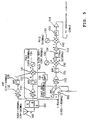
- Figure 1 shows an embodiment in a signal processing circuit for a DAB system terminal equipment that receives and reproduces an L-band signal and VHF-band signal.
- reference numeral 101 indicates a deplexer (separation network) which separately extracts a VHF-band signal of 174 - 245 MHz and an L-band signal of 1,452 - 1,492 MHz form a received signal received by an antenna 100;
- reference numeral 102 indicates a signal switcher;
- reference numerals 111, 112 and 114 indicate LNAs (low-noise amplifiers);
- reference numeral 113 indicates an automatic gain controlled (AGC) amplifier;
- reference numerals 121, 122, 123, 124 and 125 indicate band-pass;
- reference numerals 131, 132 and 133 indicate PLL (phase-locked loop) circuits which generate local oscillating signals of predetermined frequencies as local oscillators;
- reference numerals 141, 142 and 143 indicate mixers which combine said received signal and local oscillating signals generated from said PLL circuits.
- Said deplexer (branching filter) 101 is composed of, for example, a band-pass filter that passes a desired VHF-band signal and a band-pass filter that passes a desired L-band signal.
- Said low-noise amplifiers 111 and 112 are public known signal amplifiers designed to have a gain of approximately 13 dB comprising transistors, capacitors, inductors, and resistors wherein said transistors have a low NF (noise factor) index i.e.; a low noise performance in a high frequency.
- band-pass filters 121 - 125 only the filter 124 placed at the rear-end of said mixer 142 is a SAW filter having a pass-band approximately 1 MHz using a surface acoustic wave device, and other filters 121 - 123 and 125 are either ordinary band-pass filters composed of inductors (coils), capacitors, and resistors, or narrow-band band-pass filters composed of a surface acoustic wave devices.
- Said mixers 141 - 143 output a superposed signal produced by overlaying two signals: one signal on a frequency equivalent to the sum-frequency of the received signal frequency and the local oscillating signal frequency, and the other signal on a frequency equivalent to the differential-frequency between these two frequencies.
- said band-pass filters 122, 124 and 125 respectively placed at the rear-end of said mixers 141, 142 and 143 selectively pass one of said signals either on said sum-frequency or on said differential-frequency. More concretely, the pass-band of each of said filters 122, 124 and 125 is set so that the band-pass filter 122 may pass the signal on said sum-frequency and the band-pass filters 124 and 125 may pass the signal on said differential-frequency.
- said PLL circuit 131 is composed to generate a local oscillating signal of 1,269.992 MHz; VHF-band signals of 174 - 245 MHz received by said antenna 100 and separated by said deplexer (branching filter) 101 is amplified by said low-noise amplifier 111, processed in said band-pass filter 121 for noise elimination, and up-converted in a first mixer 141 by being combined with said local oscillating signal of 1,269.992 MHz generated from said PLL circuit 131.
- the first mixer 141 outputs a superposed signal produced by overlaying two signals: one signal on 1,443.992 - 1,514.992 MHz equivalent to the sum-frequency of the received signal frequency and said local oscillating signal frequency, and the other signal on 1,095.992 - 1,024.992 MHz equivalent to the differential-frequency between these two frequencies. And then, only said converted signal of 1,443.992 - 1,514.992 MHz close to L-band is sent out to the signal switcher 102 passing through said band-pass filter 122.
- Said VHF-band signal thus up-converted is selected by said signal switcher 102 for amplification by said low-noise amplifier 112 followed by processing in said band-pass filter 123 for noise elimination, and is converted into an intermediate frequency signal (IF signal) of 213 MHz in a second mixer 142 by being combined with said local oscillating signal of 1,230.992 - 1,301.992 MHz which is generated from said PLL circuit 132.
- IF signal intermediate frequency signal
- said intermediate frequency signal is processed in a narrow-band band-pass filter 124, like a SAW filter, for elimination of both noise and other interfering signals followed by processing in a third mixer 143 for conversion into a signal of 2 MHz by being combined with a local oscillating signal of 215 MHz generated from said PLL circuit 133, then is sent out to a demodulating circuit.
- a narrow-band band-pass filter 124 like a SAW filter
- the oscillating frequency of the PLL circuit 132 is variable. This comes from that, because of a narrowness of the pass-band of said SAW filter 124 placed rear-end of said second mixer 142, the oscillating signal frequency generated from said PLL circuit 132 must be variable so that all the received signal in a variety of channel frequencies may be converted into said intermediate frequency signal of 213 MHz.
- the local oscillating signal frequency at which said PLL circuit 132 should be locked is fed from a microcomputer or the like, which controls each part of the circuit according to a mode based on a input signal or other informing signals for a channel desired to be selected; wherein such computer or the like is not shown in referred Figures for simplicity.
- Said signal switcher 102 selectively sends out a signal to said low-noise amplifier 112 selecting either the signal of the VHF-band signal up-converted in said first mixer 141 or the signal of the L-band signal separated by said deplexer (branching filter) according to a mode selected by user's manipulation of a channel selection button or the like on a operating panel.
- said band-pass filter 122 is an ordinary filtering circuit comprising an inductor (a coil), a capacitor, and a resistor.
- a frequency separation between desired signals and undesired signals becomes relatively large. That is: suppose for example, that a signal of fw on 180 MHz in 180 MHz-band channel is desired for selection wherein a signal fu on 218.928 MHz on other channel exists as shown in Figure 2(a), and that these two signals fw and fu are up-converted into two signals as shown in Figure 2(b) i.e.; one on frequency of 1,449.992 MHz fw+flo1 and the other on 1,488.92 MHz fu+flo1 by said first mixer 141 based on a local oscillating signal flo1 1,269.992 MHz, further that these up-converted signals are sent out to said second mixer 142.
- signals (fw+flo1)-fbo2 and (fu+flo1)-flo2 after conversion in said second mixer 142 based on a local oscillating signal flo2 of 1,236.992 MHz have frequencies 213 MHz and 251.928 MHz respectively, as shown in Figure 2(c).
- a circuit portion other than said band-pass filters 121 - 125 can be composed on one semiconductor chip as a semiconductor integrated circuit for receiving signal processing. Further, amplifiers 113 and 114, said PLL circuit 133, and said third mixer 143 can be included in said integration on the same chip.
- Figure 3(A) shows an approximate circuit composition diagram in a PLL circuit
- Figure 3(B) shows an embodiment of a voltage controlled oscillator (VCO ) circuit diagram.
- VCO voltage controlled oscillator
- Said PLL circuit is comprised of a voltage controlled oscillator (VCO) 301; a divider 302 which divides the signal produced said voltage-controlled oscillator 301; a divider 303 which divides a reference clock ⁇ 0 having a high accuracy fed from an oscillator like a quartz oscillator; a phase comparator 304 which compares the phase between two signals each produced by said dividers 302 and 303; an up-down controlling circuit 305 which is comprised of series-configuration MOSFETs S1 and S2 that are respectively switched by an UP signal for phase lead and a DOWN signal for phase lag generated from said phase comparator 304 depending on the phase status; and a low-pass filter 306 which averages the output potential from said up-down controlling circuit 305; wherein the output voltage from said low-pass filter 306 is fed to said voltage controlled oscillator (VCO) 301 as a controlling voltage Vc.
- Said PLL circuit 132 of which frequency is variable, is controlled in its locking frequency by controlling
- Said voltage controlled oscillator (VCO) 301 is comprised of, as shown in Figure 3(B), a variable capacitance diode 402 that functions as a variable capacitor being interposed between a control terminal 401, to which said controlling voltage Vc is applied, and a grounding point; a resonance circuit 403 composed of a coil L, and capacitors C1 and C2; an output stage 404 composed of a series connection of a resistor R1, a transistor Tr and a constant current source Ic; a biasing stage 405, comprising series resistances R2 and R3, which gives said transistor Tr a biasing point; and a stabilizing means 406 composed of a feedback capacitor C3 which is interposed between the base and emitter of said transistor Tr, and a capacitor C4 which is interposed between the emitter of the transistor Tr and a grounding point; wherein an oscillating signal having the specific frequency determined by the characteristics of said resonance circuit 403 is generated from the collector of said transistor Tr.
- a change in the controlling voltage Vc varies the capacitance of the variable capacitance diode 402, thereby a resonance frequency in the resonance circuit 403 is varied to ensure said PLL circuit to oscillate a frequency corresponding to the controlling voltage Vc.
- said system further requires that the controlling voltage Vc for said voltage controlled oscillator (VCO), shown in Figure 3(B), must be capable of being swept for an extent 0 (zero) to as much as 8 V.
- VCO voltage controlled oscillator
- VCO voltage controlled oscillator
- a SAW filter 124 placed at the rear-end of said second mixer 142 in said down-converting technique should pass a signal of 38.9 MHz
- said SAW filter 124 in said up-converting technique in this embodiment may pass a signal on higher frequency of 213 MHz. This means that said filter can be small-sized. Because the electrode distance in a SAW filter is determined proportionally to the wavelength of a signal to be passed therethrough, i.e. the higher the signal frequency therein becomes, the smaller the device thereof can be designed. Thereby, the system that uses this circuitry achieves small-sizing in its device.
- the explanation dealt with the signal processing circuit for use in a DAB system terminal equipment that handles signals in two frequency bands L-band and VHF-band it is, however, further possible to apply said circuitry to the case that handles signals in more than two frequency bands.
- FIG. 5 shows another different embodiment.
- Said embodiment has a circuitry that the circuit block in said VHF-band signal up-converting circuit comprising, as shown in Figure 1 as an embodiment, a low-noise amplifier 111, a band-pass filter 121, a PLL circuit 131, and a mixer 141 is provided with a power source switch or a current switch that are controlled by the signal for controlling said signal switcher 102.
- said circuitry has a function that a power source voltage or a current fed to the VHF-band signal up-converting circuit is cut when an L-band signal is selected by the signal switcher 102.
- the power consumption therein can be largely reduced, because a power source switch or a current feeding switch for the VHF-band signal upconverting circuit becomes being allowed for switched off when an L-band signal is selected for processing, wherein said up-converting circuit for a VHF-band signal is not required to work.
- the present invention is still applicable to a semiconductor integrated circuit for receiving signal processing to be used not only in a portable telephone but in an electronic equipment like a personal computer and an audio appliance both provided with a data communication function.
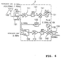
- FIG. 6 shows a further different embodiment.
- This embodiment is an embodiment of a signal processing circuit that is capable of receiving and processing both signals in wireless LAN (Local Area Network) system on 2.5 GHz and in PCS system on 1.8 GHz.
- This circuit has the same circuitry and behavior as the circuit given in Figure 1 except handling frequency. This means that the function of this circuitry is self-explanatory.
- the invention is able to realize an integrated semiconductor circuit for receiving signal processing which is capable of composing a small-sized electronic equipment with a reduced number of parts therein, and further to realize the same with low power consumption without requirement for a high voltage power source.
Landscapes
- Engineering & Computer Science (AREA)
- Computer Networks & Wireless Communication (AREA)
- Signal Processing (AREA)
- Superheterodyne Receivers (AREA)
- Circuits Of Receivers In General (AREA)
- Input Circuits Of Receivers And Coupling Of Receivers And Audio Equipment (AREA)
Applications Claiming Priority (2)
| Application Number | Priority Date | Filing Date | Title |
|---|---|---|---|
| JP22074399 | 1999-08-04 | ||
| JP11220743A JP2001044872A (ja) | 1999-08-04 | 1999-08-04 | 受信信号処理用半導体集積回路 |
Publications (2)
| Publication Number | Publication Date |
|---|---|
| EP1079531A2 true EP1079531A2 (de) | 2001-02-28 |
| EP1079531A3 EP1079531A3 (de) | 2003-11-26 |
Family
ID=16755846
Family Applications (1)
| Application Number | Title | Priority Date | Filing Date |
|---|---|---|---|
| EP00115061A Withdrawn EP1079531A3 (de) | 1999-08-04 | 2000-07-26 | Integrierte Halbleiterschaltung zur Bearbeitung von Empfangssignalen |
Country Status (2)
| Country | Link |
|---|---|
| EP (1) | EP1079531A3 (de) |
| JP (1) | JP2001044872A (de) |
Cited By (9)
| Publication number | Priority date | Publication date | Assignee | Title |
|---|---|---|---|---|
| EP1473844A1 (de) * | 2003-04-28 | 2004-11-03 | Sony Ericsson Mobile Communications AB | Analoge Eingangsschaltung für einen digitalen Zweibandempfänger mit Zwischenfrequenzabtastung |
| GB2406982A (en) * | 2003-10-10 | 2005-04-13 | Samsung Electro Mech | Down conversion of dual band (Band III / L-band) signals in Digital Audio Broadcasting |
| US7239853B2 (en) | 2002-12-06 | 2007-07-03 | Tdk Corporation | Antenna switching circuit |
| EP1282239A4 (de) * | 2001-04-06 | 2009-11-25 | Panasonic Corp | Breitband-abstimmvorrichtung |
| CN103023458A (zh) * | 2012-11-13 | 2013-04-03 | 海能达通信股份有限公司 | 有源滤波器和双工器及无线通信设备 |
| EP3094005A4 (de) * | 2014-04-24 | 2017-02-08 | Huawei Technologies Co., Ltd | Signalverarbeitungsvorrichtung, -verfahren und -system |
| EP2612535A4 (de) * | 2010-08-30 | 2017-03-29 | Samsung Electronics Co., Ltd | Vorrichtung und verfahren für einen in einem drahtlosen netzwerk betriebenen multibandfunk |
| CN111510167A (zh) * | 2020-04-09 | 2020-08-07 | 惠州Tcl移动通信有限公司 | 射频电路及终端设备 |
| CN111953358A (zh) * | 2020-08-10 | 2020-11-17 | Tcl通讯(宁波)有限公司 | 一种射频结构和移动终端 |
Families Citing this family (2)
| Publication number | Priority date | Publication date | Assignee | Title |
|---|---|---|---|---|
| US20070004363A1 (en) * | 2003-05-12 | 2007-01-04 | Takuya Kusaka | Radio lan antenna |
| CN109379102A (zh) * | 2018-12-06 | 2019-02-22 | 西南电子技术研究所(中国电子科技集团公司第十研究所) | 多通道捷变频收发装置 |
Family Cites Families (3)
| Publication number | Priority date | Publication date | Assignee | Title |
|---|---|---|---|---|
| US3961264A (en) * | 1974-05-02 | 1976-06-01 | Hekimian Laboratories, Inc. | Linear frequency converter with gain independent of circuit parameters |
| GB2058505B (en) * | 1977-07-05 | 1982-09-15 | Texas Instruments Inc | Channel selector for a television receiver |
| DE4340581C1 (de) * | 1993-11-29 | 1995-04-27 | Rohde & Schwarz | Frequenzconverter zum Erweitern des Grundempfangsbereiches eines Überlagerungsempfängers |
-
1999
- 1999-08-04 JP JP11220743A patent/JP2001044872A/ja active Pending
-
2000
- 2000-07-26 EP EP00115061A patent/EP1079531A3/de not_active Withdrawn
Cited By (14)
| Publication number | Priority date | Publication date | Assignee | Title |
|---|---|---|---|---|
| EP1282239A4 (de) * | 2001-04-06 | 2009-11-25 | Panasonic Corp | Breitband-abstimmvorrichtung |
| US7239853B2 (en) | 2002-12-06 | 2007-07-03 | Tdk Corporation | Antenna switching circuit |
| WO2004098080A1 (en) * | 2003-04-28 | 2004-11-11 | Sony Ericsson Mobile Communications Ab | Analog front end for a digital dual-band intermediate frequency sampling receiver |
| EP1473844A1 (de) * | 2003-04-28 | 2004-11-03 | Sony Ericsson Mobile Communications AB | Analoge Eingangsschaltung für einen digitalen Zweibandempfänger mit Zwischenfrequenzabtastung |
| GB2406982A (en) * | 2003-10-10 | 2005-04-13 | Samsung Electro Mech | Down conversion of dual band (Band III / L-band) signals in Digital Audio Broadcasting |
| GB2406982B (en) * | 2003-10-10 | 2006-02-22 | Samsung Electro Mech | Receiver for down-conversion of dual band for digital multimedia broadcasting or digital audio broadcasting |
| EP2612535A4 (de) * | 2010-08-30 | 2017-03-29 | Samsung Electronics Co., Ltd | Vorrichtung und verfahren für einen in einem drahtlosen netzwerk betriebenen multibandfunk |
| CN103023458A (zh) * | 2012-11-13 | 2013-04-03 | 海能达通信股份有限公司 | 有源滤波器和双工器及无线通信设备 |
| EP3094005A4 (de) * | 2014-04-24 | 2017-02-08 | Huawei Technologies Co., Ltd | Signalverarbeitungsvorrichtung, -verfahren und -system |
| US9917606B2 (en) | 2014-04-24 | 2018-03-13 | Huawei Technologies Co., Ltd. | Signal processing apparatus, method, and system |
| US10090873B2 (en) | 2014-04-24 | 2018-10-02 | Huawei Technologies Co., Ltd. | Signal processing apparatus, method, and system |
| CN111510167A (zh) * | 2020-04-09 | 2020-08-07 | 惠州Tcl移动通信有限公司 | 射频电路及终端设备 |
| CN111510167B (zh) * | 2020-04-09 | 2022-03-25 | 惠州Tcl移动通信有限公司 | 射频电路及终端设备 |
| CN111953358A (zh) * | 2020-08-10 | 2020-11-17 | Tcl通讯(宁波)有限公司 | 一种射频结构和移动终端 |
Also Published As
| Publication number | Publication date |
|---|---|
| EP1079531A3 (de) | 2003-11-26 |
| JP2001044872A (ja) | 2001-02-16 |
Similar Documents
| Publication | Publication Date | Title |
|---|---|---|
| US7756500B1 (en) | Active inductor circuits for filtering in a cable tuner circuit | |
| US6833769B2 (en) | Voltage controlled capacitive elements having a biasing network | |
| EP2139111B1 (de) | Funkwellen-Empfangsvorrichtung | |
| EP1079531A2 (de) | Integrierte Halbleiterschaltung zur Bearbeitung von Empfangssignalen | |
| US7107035B2 (en) | Frequency converter and radio communication apparatus | |
| US20090128240A1 (en) | Oscillator, pll circuit, receiver and transmitter | |
| US6795128B2 (en) | Television tuner capable of receiving FM broadcast | |
| KR100366196B1 (ko) | 발진기 | |
| US7139545B2 (en) | Ultra-wideband fully synthesized high-resolution receiver and method | |
| US20040012454A1 (en) | Wideband VCO resonant circuit method and apparatus | |
| EP0269428A2 (de) | Tuner mit FET | |
| JP2608430B2 (ja) | 同調可能な発振器 | |
| US6876401B2 (en) | FM-broadcast-receivable television tuner for preventing adjacent-channel interference | |
| JPH0738533B2 (ja) | 発振装置 | |
| US6751449B1 (en) | Circuit configuration for band changeover in high-frequency receivers | |
| EP1667347A1 (de) | Digitale Audio Rundfunk (DAB) Vorrichtungen | |
| US7286807B2 (en) | Receiver with a cascade of resonant amplifiers in the RF input stage | |
| CN101521507A (zh) | 多波段压控振荡器 | |
| JP2005184409A (ja) | 通信用半導体集積回路およびそれを搭載した電子部品 | |
| JP3591704B2 (ja) | Dab受信機 | |
| US20050266815A1 (en) | Agc circuit | |
| US7209726B2 (en) | Switch in UHF bandpass | |
| KR100446945B1 (ko) | 일정한 출력 레벨을 갖는 무조정 튜너 | |
| US6701142B1 (en) | Mixer oscillator stage | |
| WO2002041488A2 (en) | Self oscillating mixer |
Legal Events
| Date | Code | Title | Description |
|---|---|---|---|
| PUAI | Public reference made under article 153(3) epc to a published international application that has entered the european phase |
Free format text: ORIGINAL CODE: 0009012 |
|
| AK | Designated contracting states |
Kind code of ref document: A2 Designated state(s): AT BE CH CY DE DK ES FI FR GB GR IE IT LI LU MC NL PT SE |
|
| AX | Request for extension of the european patent |
Free format text: AL;LT;LV;MK;RO;SI |
|
| RAP1 | Party data changed (applicant data changed or rights of an application transferred) |
Owner name: RENESAS TECHNOLOGY EUROPE GMBH |
|
| PUAL | Search report despatched |
Free format text: ORIGINAL CODE: 0009013 |
|
| AK | Designated contracting states |
Kind code of ref document: A3 Designated state(s): AT BE CH CY DE DK ES FI FR GB GR IE IT LI LU MC NL PT SE |
|
| AX | Request for extension of the european patent |
Extension state: AL LT LV MK RO SI |
|
| 17P | Request for examination filed |
Effective date: 20040517 |
|
| AKX | Designation fees paid |
Designated state(s): DE FR GB IT |
|
| 17Q | First examination report despatched |
Effective date: 20070917 |
|
| STAA | Information on the status of an ep patent application or granted ep patent |
Free format text: STATUS: THE APPLICATION IS DEEMED TO BE WITHDRAWN |
|
| 18D | Application deemed to be withdrawn |
Effective date: 20080328 |