TECHNICAL FIELD
The present invention relates to a technique in a switching
regulator to detect and restrain inrush current at turn-on or
in the initial operation, or excessive current caused at a
short-circuit failure in the capacity for smoothing the output
voltage.
BACKGROUND ART
Generally, in a switching regulator which converts a DC
power-supply voltage into another DC voltage, the restraint
of inrush current or excessive current has been one of the
significant challenges. Here, the inrush current refers to
the current that flows abruptly to charge the capacity for
smoothing the output voltage when a switch connected to the
power source is turned on in the initial operation such as at
power-on. The excessive current, on the other hand, refers
to the current that flows excessively from the power source
towards the load when the switch connected to the power source
is in the ON state. Without restraining the inrush current
and the excessive current, the current flowing through the
inductor within the smoothing circuit would exceed the maximum
rating value, thereby causing the deterioration of the
performance or even a breakage. It must be noted that in the
present specification the inrush current and the excessive
current are collectively called inrush current except for the
case where it might be misleading.
In order to restrain the inrush current, the following
circuit structure has been suggested.
Figure 11 shows an example of the circuit structure of a
conventional switching regulator. In this example, an inrush
current detection circuit 50 includes a resistance element 51
for inrush current detection and an inrush current detector
52 which detects the presence or absence of the inrush current
by means of the voltage across the resistance element 51. The
inrush current detector 52 places the switching element 53 with
a small on resistance in the ON state in a steady operation,
and turns the element 53 off to flow the current to a resistance
element 54 for inrush current restraint upon the inrush current
detection. The resistance element 54 for inrush current
restraint is composed of a resistor with a large resistance
value or a temperature fuse resistor which interrupts a current
flow in response to overheating (Refer to Japanese Laid-Open
Patent Application No. 9-121546).
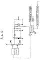
Figure 12 shows another example of the circuit structure
of the conventional switching regulator, which controls the
switching pulse width variably with a sawtooth wave in the initial
operation. Under the direction of a switch control circuit
57, a selector 56 selects and outputs the sawtooth wave in the
initial operation and a reference potential in the steady
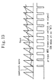
operation. Consequently, as shown in Figure 13, early in the
initial operation, the on signal of the p-type MOS transistor
switch SW1 has a short pulse width due to the comparison between
the sawtooth wave and the output voltage Vout, and later the
pulse width becomes gradually longer with increasing output
voltage Vout. As a result, the inrush current in the initial
operation is successfully restrained.
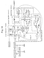
Figure 14 shows a further another example of the circuit
structure of the switching regulator which restrains the inrush
current in the initial operation by means of a sawtooth wave
in the same manner as in Figure 12. In the structure shown
in Figure 14, the on-off control of switching elements 61, 62
are done by using a loop 1 in the initial operation and a loop
2 in the steady operation. A sawtooth wave generating circuit
63 generates a sawtooth wave STW so as to perform the initializing
operation while gradually changing the switching on-off duty,
thereby restraining the inrush current in the initial operation
(Refer to Japanese Laid-Open Application No. 5-56636).
PROBLEMS TO BE SOLVED
However, the conventional switching regulator with the
above-described structures has the following problems.
The structure with the inrush current restraint circuit
shown in Figure 11 has a drawback of a low power conversion
efficiency. To be more specific, the resistance element 51
for inrush current detection causes a resistance loss because
it is interposed with a current path from the power source,
and therefore, the power conversion efficiency of the switching
regulator deteriorates.
As another drawback, the structures where the initial
operation is performed with a sawtooth wave as shown in Figures
12 and 14, it is possible to restrain the inrush current in
the initial operation; however, it is impossible to detect and
restrain the excessive current in the steady operation. There
is further another drawback of increasing the time required
for the initialization. Moreover, there is a necessity to
generate a signal that distinguishes between the initial
operation and the steady operation due to the nature of the
circuit structure.
DISCLOSURE OF THE INVENTION
The present invention has an object of providing a switching
regulator which restrains the inrush current and the excessive
current while maintaining a high power conversion efficiency
and which requires a shorter time for initialization than
conventional switching regulators.
To be more specific, a switching regulator of a synchronous
rectifying mode of the present invention comprises: a first
switch and a second switch arranged in series between a first
power source which supplies a first potential and a second power
source which supplies a second potential lower than the first
potential, the first switch being positioned closer to the first
power source than the second switch; a switch control unit for
controlling an on-off operation of the first and second switches;
and a smoothing circuit for smoothing a potential of an output
node between the first switch and the second switch, said switch
control unit turning off the first switch when the potential
of said output node is below a first reference potential which
becomes a reference to detect an occurrence of inrush current
or excessive current while the first switch is in an ON state.
According to the present invention, when the potential of
the output node goes below the first reference potential while
the first switch is in the ON state, the first switch is turned
off by regarding it as the occurrence of the inrush current
or the excessive current. To be more specific, when the
occurrence of the inrush current and the excessive current has
been detected by making use of a voltage drop due to the on
resistance of the first switch, the first switch is turned off
so as to interrupt the inrush or excessive current. This
approach can realize the detection of the inrush or excessive
current without setting up a resistance element for detection
or without causing a decrease in the power conversion efficiency
of the switching regulator. Moreover, the initial operation
does not need a different control from the steady operation,
which makes it possible to restrain the inrush current in the
initial operation and the excessive current in the steady
operation in the same manner.
The switch control unit of the switching regulator of the
present invention preferably comprises: a first reference
potential generating circuit for generating the first reference
potential; a first potential comparator for comparing the first
reference potential generated by the first reference potential
generating circuit with the potential of said output node; and
an available period setting circuit for setting an available
period during which the comparison results of the first potential
comparator is valid. The switch control unit turns off the
first switch when the first potential comparator detects that
the potential of said output node is below the first reference
potential during said available period set by said available
period setting circuit.
It is also preferable that the available period setting
circuit sets the start of said available period at a time when
a predetermined time period has elapsed since the first switch
is turned on.
It is further preferable that after turning off the first
switch, said switch control unit places the second switch in
the ON state for a predetermined time period before the first
switch is turned back on.
Consequently, while the first switch is in the OFF state,
the second switch can be placed in the ON state for a predetermined
time period to flow a current from the second power source towards
the smoothing circuit. Therefore, in the initial operation,
the time required to boost the output voltage of the smoothing
circuit to a preset voltage or the time required for
initialization can be accelerated.
The predetermined time period is preferably set at a fixed
time period. In addition, The predetermined time period is
preferably set variable in accordance with an output voltage
of said smoothing circuit.
It is also preferable that the switch control unit turns
off the second switch when the potential of said output node
exceeds a second reference potential which becomes the reference
to determine the termination of the ON-time-period of the second
switch while the second switch is in the ON state.
The LSI system of the present invention comprises: said
switching regulator of claim 1 and an LSI core unit driven by
a voltage supplied from said switching regulator.
The DC/DC converter of the present invention comprises:
a first switch and a second switch arranged in series between
a first power source which supplies a first potential and a
second power source which supplies a second potential lower
than the first potential, the first switch being positioned
closer to the first power source than the second switch; and
a switch control unit for controlling the on-off operation of
the first and second switches. The switch control unit turns
off the first switch when the potential of said output node
is below a first reference potential which becomes the reference
to detect the occurrence of inrush current or excessive current
while the first switch is in the ON state.
BRIEF DESCRIPTION OF THE DRAWINGS
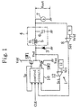
Figure 1 shows the structure of the switching regulator
of the embodiment of the present invention.
Figure 2 shows the behavior of the switching regulator of
Figure 1.
Figures 3 (a) and 3 (b) are graphs depicting a time-varying
inductor current IL in the initial operation; Figure 3 (a) shows
the embodiment of the present invention and Figure 3 (b) shows
the conventional structure.
Figure 4 shows the internal structure of the control circuit
of the switching regulator shown of Figure 1.
Figure 5 shows the behavior of the switching regulator of
Figure 1 and explains the setting of the available period.
Figure 6 shows another circuit structure of the
ON-time-period setting circuit in the control circuit of Figure
5.
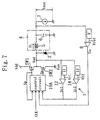
Figure 7 shows a modified example of the circuit structure
of the switching regulator of Figure 1.
Figure 8 shows the behavior of the switching regulator of
Figure 7.
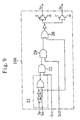
Figure 9 shows the internal structure of the control circuit
of the switching regulator of Figure 7.
Figure 10 shows an example of an LSI system provided with
the switching regulator of the present invention.
Figure 11 shows an example of the circuit structure of the
conventional switching regulator.
Figure 12 shows another example of the circuit structure
of the conventional switching regulator.
Figure 13 shows the initial operation of the switching
regulator of Figure 12.
Figure 14 shows further another example of the circuit
structure of the conventional switching regulator.
BEST MODE FOR CARRYING OUT THE INVENTION
Figure 1 shows the structure of the switching regulator
of the embodiment of the present invention. The switching
regulator comprises a first switch SW1 composed of a p-type
MOS transistor and a second switch SW2 composed of an n-type
MOS transistor which are arranged in series between a first
power source (hereinafter referred to as power source Vdd) to
supply power-supply voltage Vdd as the first potential and a
second power source (hereinafter referred to as power source
Vss) to supply a ground potential Vss as the second potential,
a diode 3 which flows a current from the power source Vss when
the first and second switches SW1, SW2 are both in the OFF state,
and a smoothing circuit 4 which smoothes the potential Vnd of
the output node between the first and second switches SW1 and
SW2. The smoothing circuit 4 is composed of an inductor 5 and
a capacity 6 for smoothing output voltage, and smoothes the
potential Vnd which has shaped a rectangular wave as a result
of the switching operation of the first and second switches
SW1, SW2 into a constant voltage. The voltage smoothed by the
smoothing circuit 4 is supplied to an output load 7 as the output
voltage Vout.
The switching regulator further comprises a control circuit
10 which controls the switching operation of the first and second
switches SW1 and SW2 using a first and second switching signals
Sp and Sn, a first reference potential generating circuit 11
which generates a first reference potential Vr1 as the reference
to detect inrush current, and a first potential comparator 12
which compares the first reference potential Vr1 generated by
the first reference potential generating circuit 11 with the
output node potential Vnd. The control circuit 10, the first
reference potential generating circuit 11 and the first
potential comparator 12 compose a switch control unit 1. The
first and second switches SW1 and SW2, the switch control unit
1, the diode 3 and the smoothing circuit 4 compose the switching
regulator of the present embodiment.
The feature of the present embodiment is to detect the
presence or absence of the occurrence of inrush current by making
use of a voltage drop due to the on resistance of the first
switch SW1. The control circuit 10 basically controls the
switching operation of the first and second switches SW1, SW2
based on a control signal Sdt indicating the results of the
comparison between the output voltage Vout and a reference
voltage Vref generated by a reference voltage generating circuit
9, and further controls inrush current restraint based on a
first determination signal Sc1 outputted from the first
potential comparator 12.
The behavior of the switching regulator shown in Figure
1 will be described as follows. First, the initial operation
will be described with reference to Figure 2. Assume that before
the initial operation, the capacity 6 for smoothing output
voltage is not charged.
First, the control circuit 10 makes the first switching
signal Sp a low ("L") to turn on the first switch SW1 (A in
Figure 2), and as a result, a current flows from the power source
Vdd towards the smoothing circuit 4 so as to start charging
the capacity 6. At this moment, inrush current occurs (B in
Figure 2). The inrush current flows from the power source Vdd
via the first switch SW1, so that due to the whole resistance
component Rp existing from the power source Vdd to the output
node including the on resistance of the first switch SW1, the
output node potential Vnd drops from the power-supply voltage
Vdd by a voltage Vdrop (C in Figure 2) which is expressed as
follows:
Vdrop = Rp × I
In the formula (1), I represents the current value of the
inrush current.
When the first determination signal Sc1 indicates that the
output node potential Vnd goes below the first reference
potential Vr1, or that the signal Sc1 becomes a high ("H") within
a set available period (which will be detailed later), the control
circuit 10 forcibly turns off the first switch SW1 on the
assumption that the inrush current has exceeded the set limit.
Consequently, the output node potential Vnd suddenly drops
below the ground potential. Vss (D in Figure 2) so as to turn
on the diode 3, which in turn makes the current flow from the
power source Vss towards the smoothing circuit 4. At this moment
in order to reduce a loss in the diode 3, the control circuit
10 places the second switch SW2 in the ON state for a predetermined
time period (E in Figure 2). As a result, the current IL flows
less and less through the inductor 5. After turning off the
second switch SW2, the control circuit 10 turns the first switch
SW1 back on (F In Figure 2). At this time, in the same manner
as above, when the first determination signal. Sc1 indicates
that the output node potential Vnd goes below the first reference
potential Vr1, or that the signal Sc1 becomes "H" within the
available period (G in Figure 2), the control circuit 10 turns
off the switch SW1, and then places the second switch SW2 in
the ON state for the predetermined time period.
By repeating these operations, the initializing operation
can be performed with restrained inrush current.
In the steady operation, the control circuit 10 behaves
as follows. The control signal Sdt indicating the results of
the comparison between the output voltage Vout and the reference
voltage Vref is fed back to the control circuit 10 where the
first switch SW1 and the second switch SW2 are alternately turned
on and off based on a PWM control system. Consequently, the
output voltage Vout is kept constant. In this case as well,
when the first determination signal Sc1 indicates that the output
node potential Vnd goes below the first reference potential
Vr1, the control circuit 10 turns off the first switch SW1 to
restrain excessive current.
As described hereinbefore, according to the present
embodiment, the inrush current can be detected and restrained
without providing a resistance element, thereby making it
possible to maintain high power conversion efficiency.
In addition, the time required for the initialization is
drastically reduced. Figures 3 (a) and 3 (b) are graphs showing
the time-varying inductor current IL in the initial operation:
Figure 3 (a) shows the present embodiment and Figure 3 (b) shows
the conventional structures with the sawtooth wave as shown
in Figures 12 and 14. As shown in Figure 3 (a), in the present
embodiment, the initial operation can be performed while flowing
the current IL through the inductor 5 nearly at the set upper
limit value. The time required for the initialization, which
is the time necessary to supply the amount of charge
(corresponding to the diagonally shaded area in Figure 3) to
the capacity 6 for smoothing output voltage, can be greatly
reduced in the present embodiment as is shown in Figure 3.
Figure 4 shows the internal structure of the control circuit
10. The control circuit 10 comprises an available period
setting circuit 21 which sets the available period of the first
determination signal Sc1 and an ON-time-period setting circuit
23 which sets the ON-time-period of the second switch SW2.
In the steady operation, the output signal of the
ON-time-period setting circuit 23 remains "L", and the output
signal of the OR gate 26 becomes equal to the control signal
Sdt. In other words, when there is no occurrence of inrush
current, the control circuit 10 controls the switching operation
of the first and second switches SW1 and SW2 according to the
control signal Sdt.
An available period signal Sv1 outputted from the available
period setting circuit 21 becomes "H" only when the inputs of
a NOR gate 21a are all lows. To be more specific, the available
period signal Sv1 becomes "H" by lagging only behind a signal
propagation time of the inverter 21b after the first switching
signal Sp becomes "L", and becomes "L" when the first switching
signal Sp becomes "H". The available period is when the
available period signal Sv1 is "H". When the control signal
Sc1 becomes "H" while the signal Sv1 is "H", the output of the
AND gate 22 becomes "H". When the output of the AND gate 22
becomes "H", the ON-time-period setting circuit 23 makes its
output "H" for the time period set by the counter 25. As a
result, regardless of the logical level of the control signal
Sdt, the output signal of the OR gate 26 becomes "H" for a fixed
time period, thereby placing the second switch SW2 in the ON
state for the fixed time period.
(SETTING THE AVAILABLE PERIOD)
Figure 5 shows the behavior of the switching regulator of
Figure 1 and explains the setting of the available period during
which the first determination signal Sc1 is valid. In Figure
5, (1) and (2) indicate the voltage and signal waveforms when
inrush current occurs, while (3) indicates the voltage and signal
waveforms when no inrush current occurs.
First, the case of (1) will be described as follows. The
control circuit 10 makes the first switching signal Sp "L" to
place the first switch SW1 in the ON state (H in Figure 5).
Consequently, the output node potential Vnd grows to reach the
power-supply potential Vdd, during which the potential Vnd
exceeds the first reference potential Vr1 (I in Figure 5) to
make the first determination signal Sc1 "L". On the other hand,
the delay signal Sp-delay of the first switching signal Sp becomes
"L" by lagging only behind the signal propagation time of the
two inverters 21b (J in Figure 5). As a result, the available
period signal Sve becomes "H" with a delay time corresponding
to the signal propagation time of the two inverters 21b after
the first switching signal Sp becomes "L". The time required
for the output node potential Vnd to exceed the first reference
potential Vr1 depends on the load current value, or the charge
status of the capacity 6, that is, the output voltage Vout.
Therefore, the delay time of the available period signal Sve
must be set long enough to secure that the output node potential
Vnd exceeds the first reference potential Vr1 by the start of
the available period.
When the inrush current flows while the available period
signal Sve is "H" (K in Figure 5) to make the output node potential
Vnd go below the first reference potential Vr1 (L in Figure
5), the first determination signal Sc1 becomes "H" (M in Figure
5), and the control circuit 10 forces the first switching signal
Sp to be "H" so as to turn off the first switch SW1 (N in Figure
5). As a result of the first switch SW1 having been turned
off, the available period signal Sve immediately becomes "L"
to terminate the available period.
The case of (2) will be described as follows. The control
circuit 10 makes the first switching signal Sp "L" to turn on
the first switch SW1 (O in Figure 5). Consequently, the output
node potential Vnd increases; however, when the inrush or
excessive current is already flowing, the output node potential
Vnd does not reach the first reference potential Vr1 (P in Figure
5). At this time, the control circuit 10 immediately turns
off the first switch SW1 because the first determination signal
Sc1 remains to be "H" (R in Figure 5) when the available period
signal Sve becomes "H" (Q in Figure 5). Since the first switch
SW1 is in the ON state only during the signal propagation time
of the two inverters 21b after the first switching signal Sp
becomes "L", the first reference potential Vr1 must be set with
some margins by taking the inrush current which flows during
this time period into account.
The case of (3) will be described as follows. In the same
manner as the cases of (1) and (2), the control circuit 10 makes
the first switching signal Sp "L" to turn on the first switch
SW1 (T in Figure 5). As a result, the output node potential
Vnd grows to reach the power-supply potential Vdd. In this
process, the output node potential Vnd exceeds the first
reference potential Vr1, and the determination signal Sc1
becomes "L". Later, the available period signal Sve becomes
"H" (U in Figure 5). However, in the steady operation where
no inrush occurs, the output node potential Vnd does not go
below the first reference potential Vr1 (V in Figure 5), so
that the first determination signal Sc1 remains "L". The
control circuit 10 makes the first switching signal Sp "H" in
accordance with the control signal Sdt to turn off the first
switch SW1 (W in Figure 5). Accordingly, the available period
signal Sve also becomes "L" immediately. Later, even when the
first determination signal Sc1 becomes "H" (X in Figure 5),
the switching regulator can continue the steady operation
because the available period signal Sve is "L".
Thus, providing the available period realizes the detection
of both the Inrush current in the initial operation and the
excessive current in the steady operation.
(SETTING OF THE ON-TIME-PERIOD OF THE SECOND SWITCH SW2)
When the ON-time-period of the second switch SW2 is too
long, the current IL flows less and less through the inductor
5 and finally flows in the reverse direction. This prevents
the output voltage Vout from growing, which results in the
extension of the time required for the initialization.
On the other hand, if the ON-time-period of the second switch
SW2 is too short, when the first switch SW1 is turned on next
time, the current IL flowing through the inductor 5 is
sufficiently large, so that the first switch SW1 must be turned
off immediately as shown in (2) in Figure 5. Therefore, the
first reference potential Vr1 must be provided with enough
margins by taking the inrush current flowing during the
ON-time-period into consideration. Moreover, the next
ON-time-period of the first switch SW1 also becomes short, so
that the switching period becomes short, making the resultant
charge-discharge loss not negligible. Thus, the
ON-time-period of the second switch SW2 is a very important
factor to the time required for the initialization and to the
efficiency.
Therefore, in the present embodiment, the ON-time-period
of the second switch SW2 is set as follows. The rate of decrease
in the current IL flowing through the inductor 5 in the
ON-time-period of the second switch SW2 depends on the voltage
across the inductor 5 or the difference between the output node
potential Vnd and the output voltage Vout (approximately
corresponding to the output voltage Vout). In view of this,
when the output voltage Vout is low, a certain time period during
which the current IL flowing through the inductor 5 fully falls
is set as the ON-time-period of the second switch SW2. To be
more specific, the ON-time-period is set as the time required
to sufficiently decrease the amount of the current IL flowing
through the inductor 5 to the value which allows the output
node potential Vnd to exceed the first reference potential Vr1
when the first switch SW1 is turned back on.
Alternatively, the ON-time-period of the second switch SW2
can be set to be variable in accordance with the output voltage
Vout.
The rate of decrease in the current IL flowing through the
inductor 7 when the second switch SW2 is in the ON state is
small when the output voltage Vout is low, and large when it
is high. Judging from this, in the initial operation, it is
preferable that when the output voltage Vout is low, the
ON-time-period of the second switch SW2 should be set long and
made gradually shorter with the output voltage Vout increasing.
The ON-time-period of the second switch SW2 at the beginning
of the initial operation can be set in the above-mentioned time
period. Setting the ON-time-period of the second switch SW2
variable like this In accordance with the output voltage Vout
achieves the reduction of the time required for the
initialization.
Figure
6 shows the circuit structure of the ON-time-period
setting circuit to realize the above-mentioned control. The
ON-time-
period setting circuit 23A shown in Figure
6 comprises
four
counters 25a to
25d to which four different ON-time-periods
such as 4µs, 3µs, 2µs and 1 µs can be set respectively. The
values of signals A and B can be set as shown in Table
1 below
according to the output voltage Vout.
| Vout | A | B | ON-time-period |
| 0∼ 500 mV | L | L | 4µS |
| 500 ∼ 1 V | H | L | 3µS |
| 1V ∼ 2 V | L | H | 2µS |
| 2 V ∼ | H | H | 1µs |
Figure 7 shows the circuit structure of a modified example
of the switching regulator of the present embodiment. In Figure
7, like components are labeled with like reference numerals
with respect to Figure 1. The switching regulator comprises
a second reference potential generating circuit 13 which
generates a second reference potential Vr2 as the reference
to determine the termination of the ON-time-period of the second
switch SW2 and a second potential comparator circuit 14 which
compares the output node potential Vnd with the second reference
potential Vr2. A switch control unit 2 is composed of a control
circuit 10A, the first and second reference potential generating
circuits 11, 13 and the first and second potential comparator
circuits 12, 14.
The feature of the modified example is to place the second
switch SW2 in the ON state until the output node potential Vnd
reaches the second reference potential Vr2, instead of
previously setting the ON-time-period of the second switch SW2
at a predetermined time period. The control circuit 10A
basically controls the switching operation of the first and
second switches SW1 and SW2, based on the control signal Sdt
indicating the results of the comparison between the output
voltage Vout and the reference voltage Vref generated by the
reference voltage generating circuit 9. The control circuit
10A further controls the restraint of the inrush current based
on the first determination signal Sc1 outputted from the first
potential comparator 12 and sets the termination of the
ON-time-period of the second switch SW2 based on the second
determination signal Sc2 outputted from the second potential
comparator 14.
The behavior of the switching regulator shown in Figure
7 will be described as follows with reference to Figure 8. When
the inrush current or the excessive current flows to make the
output node potential Vnd go below the first reference potential
Vr1 within the available period (A in Figure 8), the control
circuit 10A detects that the first determination signal Sc1
is "H" and makes the first switching signal Sp "H" to turn off
the first switch SW1 (B shown in Figure 8). Later, the control
circuit 10A makes the second switching signal Sn "H" so as to
turn on the second switch SW2, but the ON-time-period is not
set in advance. When the output node potential Vnd exceeds
the second reference potential Vr2 (C in Figure 8), the second
determination signal Sc2 becomes "H", and the control circuit
10A detects that the second determination signal Sc2 is "H"
and makes the second switching signal Sn "L" so as to turn off
the second switch SW2 (D in Figure 8).
In order to quicken the initial operation of the switching
regulator, it is preferable that the ON-time-period of the second
switch SW2 is as long as possible within a range where the output
node potential Vnd does not exceed the ground potential Vss.
Therefore, as in this modified example, the termination of the
ON-time-period of the second switch SW2 can be determined by
the comparison between the output node potential Vnd and the
second reference potential Vr1 so as to reduce the time required
for the initialization, while inrush current being restrained.
It goes without saying that the inrush current or the
excessive current can be restrained both in the initial operation
and in the steady operation.
Figure 9 shows the circuit structure of the control circuit
10A of Figure 7. In Figure 9, like components are labeled with
like reference numerals with respect to Figure 4 showing the
circuit structure of the control circuit 10 of Figure 1. In
Figure 9, the ON-time-period setting circuit 23 of Figure 4
is replaced by a 2-input NAND gate 29 which enters the second
determination signal Sc2 and the output signal of the NAND gate
22.
In the above-mentioned embodiment or the modified example,
the first reference potential Vr1 may be so structured that
the setting is changeable. This can extend the range of choices
of the inductor 5 in the smoothing circuit 4 and improve the
flexibility of design in the system. It is also possible to
make the second reference potential Vr2 changeable in setting.
Figure 10 shows an example of the LSI system provided with
the switching regulator of the present invention. The LSI 30
comprises an LSI core unit 31 and a DC/DC converter 32, and
further comprises a diode 3 and a smoothing circuit 4 as external
components. There are also pads 33a to 33c. The DC/DC converter
32 comprises the first and second switches SW1, SW2 and the
switch control unit 1 or 2 shown in the above-mentioned embodiment
or the modified example. The switching regulator of the present
invention is composed of the DC/DC converter 32, the diode 3
and the smoothing circuit 4. The DC/DC converter 32 converts
the power-supply potentials Vdd, Vss supplied to the pads 33a,
33b into the voltage Vnd through the behavior of the
above-mentioned embodiment or the modified example to output
it to the pad 33c. The smoothing circuit 4 smoothes the output
voltage Vnd of the DC/DC converter 32 and outputs it as the
voltage Vout. The output voltage Vout of the smoothing circuit
4 is supplied as the internal power-supply voltage of the LSI
core unit 31.
As described hereinbefore, according to the present
invention, the occurrence of inrush current is detected by making
use of a voltage drop due to the on resistance of the first
switch, so that the detection of the inrush current can be
realized without providing a resistance element for detection,
that is, without causing a decrease in the power conversion
efficiency of the switching regulator. Moreover, excessive
current in the steady operation can be restrained in the same
manner as the inrush current in the initial operation because
the initial operation does not need to be controlled differently
from in the steady operation.
Furthermore, it is possible to reduce the time required
for the initialization by placing the second switch in the ON
state for a predetermined time period while the first switch
is in the OFF state.