EP1077466A2 - Flache Plasma-Anzeigetafel mit gesteuerten Plasma-Auferechterhaltungselektroden - Google Patents
Flache Plasma-Anzeigetafel mit gesteuerten Plasma-Auferechterhaltungselektroden Download PDFInfo
- Publication number
- EP1077466A2 EP1077466A2 EP00117638A EP00117638A EP1077466A2 EP 1077466 A2 EP1077466 A2 EP 1077466A2 EP 00117638 A EP00117638 A EP 00117638A EP 00117638 A EP00117638 A EP 00117638A EP 1077466 A2 EP1077466 A2 EP 1077466A2
- Authority
- EP
- European Patent Office
- Prior art keywords
- electrodes
- voltage
- sustaining
- auxiliary
- substrate
- Prior art date
- Legal status (The legal status is an assumption and is not a legal conclusion. Google has not performed a legal analysis and makes no representation as to the accuracy of the status listed.)
- Withdrawn
Links
Images


Classifications
-
- H—ELECTRICITY
- H01—ELECTRIC ELEMENTS
- H01J—ELECTRIC DISCHARGE TUBES OR DISCHARGE LAMPS
- H01J11/00—Gas-filled discharge tubes with alternating current induction of the discharge, e.g. alternating current plasma display panels [AC-PDP]; Gas-filled discharge tubes without any main electrode inside the vessel; Gas-filled discharge tubes with at least one main electrode outside the vessel
- H01J11/20—Constructional details
- H01J11/22—Electrodes, e.g. special shape, material or configuration
- H01J11/24—Sustain electrodes or scan electrodes
-
- H—ELECTRICITY
- H01—ELECTRIC ELEMENTS
- H01J—ELECTRIC DISCHARGE TUBES OR DISCHARGE LAMPS
- H01J11/00—Gas-filled discharge tubes with alternating current induction of the discharge, e.g. alternating current plasma display panels [AC-PDP]; Gas-filled discharge tubes without any main electrode inside the vessel; Gas-filled discharge tubes with at least one main electrode outside the vessel
- H01J11/20—Constructional details
- H01J11/22—Electrodes, e.g. special shape, material or configuration
- H01J11/28—Auxiliary electrodes, e.g. priming electrodes or trigger electrodes
-
- G—PHYSICS
- G09—EDUCATION; CRYPTOGRAPHY; DISPLAY; ADVERTISING; SEALS
- G09G—ARRANGEMENTS OR CIRCUITS FOR CONTROL OF INDICATING DEVICES USING STATIC MEANS TO PRESENT VARIABLE INFORMATION
- G09G3/00—Control arrangements or circuits, of interest only in connection with visual indicators other than cathode-ray tubes
- G09G3/20—Control arrangements or circuits, of interest only in connection with visual indicators other than cathode-ray tubes for presentation of an assembly of a number of characters, e.g. a page, by composing the assembly by combination of individual elements arranged in a matrix no fixed position being assigned to or needed to be assigned to the individual characters or partial characters
- G09G3/22—Control arrangements or circuits, of interest only in connection with visual indicators other than cathode-ray tubes for presentation of an assembly of a number of characters, e.g. a page, by composing the assembly by combination of individual elements arranged in a matrix no fixed position being assigned to or needed to be assigned to the individual characters or partial characters using controlled light sources
- G09G3/28—Control arrangements or circuits, of interest only in connection with visual indicators other than cathode-ray tubes for presentation of an assembly of a number of characters, e.g. a page, by composing the assembly by combination of individual elements arranged in a matrix no fixed position being assigned to or needed to be assigned to the individual characters or partial characters using controlled light sources using luminous gas-discharge panels, e.g. plasma panels
- G09G3/288—Control arrangements or circuits, of interest only in connection with visual indicators other than cathode-ray tubes for presentation of an assembly of a number of characters, e.g. a page, by composing the assembly by combination of individual elements arranged in a matrix no fixed position being assigned to or needed to be assigned to the individual characters or partial characters using controlled light sources using luminous gas-discharge panels, e.g. plasma panels using AC panels
- G09G3/298—Control arrangements or circuits, of interest only in connection with visual indicators other than cathode-ray tubes for presentation of an assembly of a number of characters, e.g. a page, by composing the assembly by combination of individual elements arranged in a matrix no fixed position being assigned to or needed to be assigned to the individual characters or partial characters using controlled light sources using luminous gas-discharge panels, e.g. plasma panels using AC panels using surface discharge panels
- G09G3/2983—Control arrangements or circuits, of interest only in connection with visual indicators other than cathode-ray tubes for presentation of an assembly of a number of characters, e.g. a page, by composing the assembly by combination of individual elements arranged in a matrix no fixed position being assigned to or needed to be assigned to the individual characters or partial characters using controlled light sources using luminous gas-discharge panels, e.g. plasma panels using AC panels using surface discharge panels using non-standard pixel electrode arrangements
- G09G3/2986—Control arrangements or circuits, of interest only in connection with visual indicators other than cathode-ray tubes for presentation of an assembly of a number of characters, e.g. a page, by composing the assembly by combination of individual elements arranged in a matrix no fixed position being assigned to or needed to be assigned to the individual characters or partial characters using controlled light sources using luminous gas-discharge panels, e.g. plasma panels using AC panels using surface discharge panels using non-standard pixel electrode arrangements with more than 3 electrodes involved in the operation
-
- H—ELECTRICITY
- H01—ELECTRIC ELEMENTS
- H01J—ELECTRIC DISCHARGE TUBES OR DISCHARGE LAMPS
- H01J11/00—Gas-filled discharge tubes with alternating current induction of the discharge, e.g. alternating current plasma display panels [AC-PDP]; Gas-filled discharge tubes without any main electrode inside the vessel; Gas-filled discharge tubes with at least one main electrode outside the vessel
- H01J11/10—AC-PDPs with at least one main electrode being out of contact with the plasma
- H01J11/12—AC-PDPs with at least one main electrode being out of contact with the plasma with main electrodes provided on both sides of the discharge space
-
- H—ELECTRICITY
- H01—ELECTRIC ELEMENTS
- H01J—ELECTRIC DISCHARGE TUBES OR DISCHARGE LAMPS
- H01J11/00—Gas-filled discharge tubes with alternating current induction of the discharge, e.g. alternating current plasma display panels [AC-PDP]; Gas-filled discharge tubes without any main electrode inside the vessel; Gas-filled discharge tubes with at least one main electrode outside the vessel
- H01J11/20—Constructional details
- H01J11/34—Vessels, containers or parts thereof, e.g. substrates
- H01J11/38—Dielectric or insulating layers
-
- H—ELECTRICITY
- H01—ELECTRIC ELEMENTS
- H01J—ELECTRIC DISCHARGE TUBES OR DISCHARGE LAMPS
- H01J11/00—Gas-filled discharge tubes with alternating current induction of the discharge, e.g. alternating current plasma display panels [AC-PDP]; Gas-filled discharge tubes without any main electrode inside the vessel; Gas-filled discharge tubes with at least one main electrode outside the vessel
- H01J11/20—Constructional details
- H01J11/34—Vessels, containers or parts thereof, e.g. substrates
- H01J11/42—Fluorescent layers
-
- G—PHYSICS
- G09—EDUCATION; CRYPTOGRAPHY; DISPLAY; ADVERTISING; SEALS
- G09G—ARRANGEMENTS OR CIRCUITS FOR CONTROL OF INDICATING DEVICES USING STATIC MEANS TO PRESENT VARIABLE INFORMATION
- G09G2320/00—Control of display operating conditions
- G09G2320/02—Improving the quality of display appearance
- G09G2320/0228—Increasing the driving margin in plasma displays
-
- H—ELECTRICITY
- H01—ELECTRIC ELEMENTS
- H01J—ELECTRIC DISCHARGE TUBES OR DISCHARGE LAMPS
- H01J2211/00—Plasma display panels with alternate current induction of the discharge, e.g. AC-PDPs
- H01J2211/20—Constructional details
- H01J2211/22—Electrodes
- H01J2211/32—Disposition of the electrodes
- H01J2211/323—Mutual disposition of electrodes
Definitions
- This invention relates in general to a flat-panel display and in particular to an improved structure for a full color, high resolution capable flat-panel display which operates at a high efficiency.
- the basic structure of an AC Plasma Display Panel, or PDP comprises two glass plates with a conductor pattern of electrodes on the inner surfaces of each plate.
- the plates are separated by a gas filled gap.
- the electrodes are configured in an x-y matrix with the electrodes on each plate deposited at right angles to each other using conventional thin of thick film techniques.
- At least one set of sustaining electrodes of the AC PDP is covered with a thin glass dielectric layer.
- the glass plates are assembled into a sandwich with the gap between the plates fixed by spacers. The edges of the plates are sealed and the cavity between the plates is evacuated and filled with a mixture of neon and xenon gases or a similar gas mixture of a type well known in the art.
- a sufficient driver voltage pulse is applied to the electrodes to ionize the gas contained between the plates.
- the dielectrics charge like small capacitors, which reduces the voltage across the gas and extinguishes the discharge.
- the capacitive voltages are due to stored charge and are conventionally called wall charge.
- the voltage is then reversed, and the sum of the driver voltage and wall charge voltages is again large enough to excite the gas and produce a glow discharge pulse.
- a sequence of such driver voltages repetitively applied is called the sustaining voltage, or sustainer.
- sustainer waveform pixels which have had charge stored will discharge and emit light pulses at every sustainer cycle. Pixels which have no charge stored will not emit light.
- appropriate waveforms are applied across the x-y matrix of electrodes, small light emitting pixels form a visual picture.
- barrier ribs are typically disposed between the plates to prevent cross-color and cross-pixel interference between the electrodes.
- the barrier ribs also increase the resolution to provide a sharply defined picture.
- the barrier ribs further provide a uniform discharge space between the glass plates by utilizing the barrier rib height, width and pattern gap to achieve a desired pixel pitch.
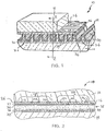
- This invention relates to an improved plasma flat-panel display which includes at least one auxiliary electrode disposed between each pair of sustaining electrodes.
- plasma flat-panel displays having pairs of sustaining electrodes which establish a charged volume between the display substrates.
- the charge is controlled by applying voltages to a plurality of address electrodes.
- the charged volume is established by applying a voltage to the sustaining electrodes.
- the efficiency of the panel is generally greater when gas and geometry parameters are adjusted to increase the voltage required to sustain a discharge.
- this is in conflict with the need to have low voltages for economic and reliability purposes. Therefore, it would be desirable to develop a compromise device which would allow initiation and control of the sustaining discharge with a less powerful and lower voltage controlling means.
- the present invention contemplates a plasma flat-panel display having a first transparent substrate with at least one pair of parallel sustaining electrodes deposited thereupon. A least one auxiliary electrode is deposited upon the first substrate parallel to the sustaining electrodes.
- the panel also includes an charge storage surface coating which covers the sustaining and auxiliary electrode.
- the panel further includes a second substrate which is hermetically sealed to the first substrate, the second substrate, having a plurality of gas-filled micro-voids formed in a surface thereof which is adjacent to the first substrate.
- the micro-voids are generally perpendicular to the sustaining and auxiliary electrodes and cooperate with the first substrate to define a plurality of sub-pixels.
- a plurality of address electrodes are incorporated within the second substrate, each of the address electrodes corresponding to one of the sub-pixels.
- a first voltage is applied to the auxiliary electrode of sufficient magnitude to inject a charge of electrons between the auxiliary electrode and an associated sustaining electrode and initiate a discharge therebetween.
- a second voltage that is greater than the first voltage is applied to the sustaining electrodes to extend the discharge to the other sustaining electrode.
- the voltage applied to the auxiliary electrode can be changed to urge the discharge deeper into the associated micro-void.
- the first voltage is applied before the second voltage; however, the invention also can be practiced with the first and second voltages being applied simultaneously or with the second voltage applied before the first voltage.
- the discharge between the sustaining electrodes can be controlled by applying a third voltage to the address electrodes.
- a phosphor material is deposited within each micro-void and associated with the address electrodes.
- the first and second substrates are formed from glass.
- the invention can be practiced having a pair of auxiliary electrodes disposed between the sustaining electrodes.
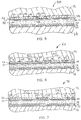
- the channels 32 are filled with a proportioned mixture of two or more ionizable gases which produces sufficient UV radiation to excite the phosphor material 38.
- a gas mixture of neon and from about five to 20 percent by weight of xenon and helium is used.
- a discharge is initiated between a selected pair of auxiliary electrodes 24 by applying a first voltage across the auxiliary electrodes. Because the auxiliary electrodes are relatively dose together, the first voltage needed to initiate the discharge is less than the voltage required to initiate a discharge between the sustaining electrodes.
- the second auxiliary electrode 66 is separated from the right sustaining electrode 64 by about 40 microns to 100 microns.
- the second set of electrodes 62 includes a pair of sustaining electrodes 67 having first and second auxiliary electrodes 68 and 69 disposed adjacent thereto.
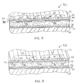
- a first voltage is applied to the first auxiliary electrode 65 which establishes a starting charge of electrons between the first auxiliary electrode 65 and the left sustaining electrode 63.
- the charge of electrons may be the result of a relatively small discharge between the auxiliary electrode 65 and a sustaining electrode 63.
- the starting charge enables establishment of a relatively larger discharge between the sustaining electrodes 63 and 64 with a lower sustaining voltage than would be needed in the absence of the starting charge.
- the sustaining electrode 63 be a cathode with respect to the auxiliary electrode 65 at this phase of the operation.
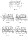
- FIG. 16 An alternate three-step method for initiating a discharge is illustrated in Figs. 16 through 19.
- a first voltage is applied between the left sustaining electrode 63 and the opposite address electrode 36.
- the left sustaining electrode 63 is negative relative to the address electrode 36 and functions as a cathode.
- An initial discharge 106 is established in Fig. 16 between the left sustaining electrode 63 and the address electrode 36.
- the initial discharge 106 is moved to the right in Fig. 17 by application of a second voltage between the left sustaining electrode 63 and the first auxiliary electrode 65 to establish the cathode fall region 102 described above.
- the operation then proceeds as described above with a third sustaining voltage applied between the sustaining electrodes 63 and 64 in Fig. 18.
Landscapes
- Engineering & Computer Science (AREA)
- Physics & Mathematics (AREA)
- Plasma & Fusion (AREA)
- Chemical & Material Sciences (AREA)
- Materials Engineering (AREA)
- Power Engineering (AREA)
- Computer Hardware Design (AREA)
- General Physics & Mathematics (AREA)
- Theoretical Computer Science (AREA)
- Gas-Filled Discharge Tubes (AREA)
- Control Of Indicators Other Than Cathode Ray Tubes (AREA)
- Control Of Gas Discharge Display Tubes (AREA)
Applications Claiming Priority (6)
| Application Number | Priority Date | Filing Date | Title |
|---|---|---|---|
| US09/376,130 US6459201B1 (en) | 1999-08-17 | 1999-08-17 | Flat-panel display with controlled sustaining electrodes |
| US376130 | 1999-08-17 | ||
| US16846999P | 1999-12-01 | 1999-12-01 | |
| US168469P | 1999-12-01 | ||
| US629118 | 2000-07-31 | ||
| US09/629,118 US6597120B1 (en) | 1999-08-17 | 2000-07-31 | Flat-panel display with controlled sustaining electrodes |
Publications (2)
| Publication Number | Publication Date |
|---|---|
| EP1077466A2 true EP1077466A2 (de) | 2001-02-21 |
| EP1077466A3 EP1077466A3 (de) | 2007-11-21 |
Family
ID=27389529
Family Applications (1)
| Application Number | Title | Priority Date | Filing Date |
|---|---|---|---|
| EP00117638A Withdrawn EP1077466A3 (de) | 1999-08-17 | 2000-08-16 | Flache Plasma-Anzeigetafel mit gesteuerten Plasma-Auferechterhaltungselektroden |
Country Status (6)
| Country | Link |
|---|---|
| US (1) | US6597120B1 (de) |
| EP (1) | EP1077466A3 (de) |
| JP (1) | JP2001195985A (de) |
| KR (1) | KR100739480B1 (de) |
| CN (1) | CN1179315C (de) |
| MX (1) | MXPA00007975A (de) |
Cited By (3)
| Publication number | Priority date | Publication date | Assignee | Title |
|---|---|---|---|---|
| KR100453161B1 (ko) * | 2001-10-24 | 2004-10-15 | 엘지전자 주식회사 | 플라즈마 디스플레이 패널 및 그의 구동방법과 그의 하판 제조방법 |
| EP1630846A1 (de) * | 2004-08-24 | 2006-03-01 | Samsung SDI Co., Ltd. | Plamabildschirm |
| EP1522987A3 (de) * | 2003-10-06 | 2006-08-23 | Lg Electronics Inc. | Verfahren zur Ansteuerung einer Plasmaanzeigetafel |
Families Citing this family (12)
| Publication number | Priority date | Publication date | Assignee | Title |
|---|---|---|---|---|
| US6597120B1 (en) * | 1999-08-17 | 2003-07-22 | Lg Electronics Inc. | Flat-panel display with controlled sustaining electrodes |
| KR20020035699A (ko) * | 2000-11-07 | 2002-05-15 | 구자홍 | 플라즈마 디스플레이 패널 및 그 구동방법 |
| KR100483988B1 (ko) | 2001-11-29 | 2005-04-15 | 삼성에스디아이 주식회사 | 투명도전막의 투과도 변형방법 |
| JP4251389B2 (ja) * | 2002-06-28 | 2009-04-08 | 株式会社日立プラズマパテントライセンシング | プラズマディスプレイパネルの駆動装置 |
| CN1813278A (zh) * | 2003-06-23 | 2006-08-02 | 松下电器产业株式会社 | 等离子体显示面板装置及其驱动方法 |
| US7511426B2 (en) * | 2004-04-22 | 2009-03-31 | The Board Of Trustees Of The University Of Illinois | Microplasma devices excited by interdigitated electrodes |
| US7573202B2 (en) * | 2004-10-04 | 2009-08-11 | The Board Of Trustees Of The University Of Illinois | Metal/dielectric multilayer microdischarge devices and arrays |
| US7477017B2 (en) | 2005-01-25 | 2009-01-13 | The Board Of Trustees Of The University Of Illinois | AC-excited microcavity discharge device and method |
| WO2006080128A1 (ja) * | 2005-01-31 | 2006-08-03 | Technology Trade And Transfer Corporation | 放電型表示装置 |
| KR100741118B1 (ko) * | 2006-02-22 | 2007-07-19 | 삼성에스디아이 주식회사 | 플라즈마 디스플레이 패널 |
| US7615926B2 (en) * | 2006-06-12 | 2009-11-10 | The Board Of Trustees Of The University Of Illinois | Low voltage microcavity plasma device and addressable arrays |
| CN106714434B (zh) * | 2015-07-17 | 2024-04-09 | 核工业西南物理研究院 | 成对电极共面放电等离子体发生装置 |
Family Cites Families (36)
| Publication number | Priority date | Publication date | Assignee | Title |
|---|---|---|---|---|
| US3559190A (en) | 1966-01-18 | 1971-01-26 | Univ Illinois | Gaseous display and memory apparatus |
| BE755591Q (fr) | 1967-11-24 | 1971-02-15 | Owens Illinois Inc | Dispositif de memorisation et de reproduction a decharges gazeuses et son mode de fonctionnement |
| US4723093A (en) | 1968-10-02 | 1988-02-02 | Owens-Illinois Television Products Inc. | Gas discharge device |
| NL7016929A (de) | 1970-11-19 | 1972-05-24 | ||
| NL7317435A (nl) | 1973-12-20 | 1975-06-24 | Philips Nv | Gasontladingspaneel. |
| US4494038A (en) | 1975-03-10 | 1985-01-15 | Owens-Illinois, Inc. | Gas discharge device |
| JPS5263663A (en) | 1975-11-19 | 1977-05-26 | Fujitsu Ltd | Gas electric discharge panel |
| DE3206104A1 (de) | 1982-02-19 | 1983-09-01 | Bayer Ag, 5090 Leverkusen | Vibrationstrennsieb an ruehrwerks-kugelmuehlen |
| US4638218A (en) | 1983-08-24 | 1987-01-20 | Fujitsu Limited | Gas discharge panel and method for driving the same |
| EP0157248B1 (de) | 1984-03-19 | 1992-06-03 | Fujitsu Limited | Verfahren zur Steuerung einer Gasentladungsanzeigevorrichtung |
| JPS6161341A (ja) | 1984-08-31 | 1986-03-29 | Fujitsu Ltd | ガス放電パネル |
| US5086297A (en) | 1988-06-14 | 1992-02-04 | Dai Nippon Insatsu Kabushiki Kaisha | Plasma display panel and method of forming fluorescent screen thereof |
| KR910020783A (ko) | 1990-05-25 | 1991-12-20 | 김정배 | 플라즈마 표시패널과 그 제조 방법 |
| KR920004143B1 (ko) | 1990-07-04 | 1992-05-25 | 삼성전관 주식회사 | 플라즈마 표시소자 |
| JP3013470B2 (ja) | 1991-02-20 | 2000-02-28 | ソニー株式会社 | 画像表示装置 |
| EP0554172B1 (de) | 1992-01-28 | 1998-04-29 | Fujitsu Limited | Plasma Farbanzeige-Vorrichtung von Oberflächenentladungs-Typ |
| US5828356A (en) | 1992-08-21 | 1998-10-27 | Photonics Systems Corporation | Plasma display gray scale drive system and method |
| US5469021A (en) | 1993-06-02 | 1995-11-21 | Btl Fellows Company, Llc | Gas discharge flat-panel display and method for making the same |
| JP3394799B2 (ja) | 1993-09-13 | 2003-04-07 | パイオニア株式会社 | プラズマディスプレイ装置 |
| JP2581465B2 (ja) * | 1994-09-28 | 1997-02-12 | 日本電気株式会社 | プラズマディスプレイパネルとその駆動方法 |
| JP2671870B2 (ja) * | 1995-05-02 | 1997-11-05 | 日本電気株式会社 | プラズマディスプレイパネル及びその駆動方法 |
| JP2716013B2 (ja) | 1995-08-11 | 1998-02-18 | 日本電気株式会社 | カラープラズマディスプレイパネルおよびその製造方法 |
| RU2089966C1 (ru) * | 1995-11-22 | 1997-09-10 | Научно-производственная компания "Орион-Плазма" - Совместная акционерная компания закрытого типа | Газоразрядная индикаторная панель переменного тока с реверсивным поверхностным разрядом |
| JPH09245627A (ja) * | 1996-03-07 | 1997-09-19 | Mitsubishi Electric Corp | ガス放電表示装置、その製造方法及びそのパネルの駆動方法 |
| US5723945A (en) | 1996-04-09 | 1998-03-03 | Electro Plasma, Inc. | Flat-panel display |
| JPH1038688A (ja) | 1996-07-24 | 1998-02-13 | Nikon Corp | 分光光度計 |
| JP3775703B2 (ja) | 1996-08-28 | 2006-05-17 | タイコエレクトロニクスアンプ株式会社 | フレキシブル回路板用コネクタ |
| KR19980046358A (ko) * | 1996-12-12 | 1998-09-15 | 엄길용 | 플라즈마 디스플레이 패널 구조 및 그 구동방법 |
| US6448946B1 (en) | 1998-01-30 | 2002-09-10 | Electro Plasma, Inc. | Plasma display and method of operation with high efficiency |
| RU2120154C1 (ru) * | 1997-03-28 | 1998-10-10 | Совместное закрытое акционерное общество "Научно-производственная компания "ОРИОН-ПЛАЗМА" | Газоразрядная индикаторная панель переменного тока с поверхностным разрядом и способ управления ею |
| JPH10333636A (ja) * | 1997-03-31 | 1998-12-18 | Mitsubishi Electric Corp | プラズマディスプレイパネル |
| JP2001039822A (ja) * | 1999-07-28 | 2001-02-13 | Mikimoto Pharmaceut Co Ltd | エラスターゼ阻害剤 |
| US6459201B1 (en) | 1999-08-17 | 2002-10-01 | Lg Electronics Inc. | Flat-panel display with controlled sustaining electrodes |
| US6597120B1 (en) * | 1999-08-17 | 2003-07-22 | Lg Electronics Inc. | Flat-panel display with controlled sustaining electrodes |
| JP2001099554A (ja) * | 1999-09-28 | 2001-04-13 | Sanyo Electric Co Ltd | 冷蔵庫 |
| KR100509601B1 (ko) * | 2000-04-28 | 2005-08-22 | 삼성에스디아이 주식회사 | 촉화전자를 제공하기 위한 보조 전극을 구비한 플라즈마디스플레이 패널 |
-
2000
- 2000-07-31 US US09/629,118 patent/US6597120B1/en not_active Expired - Fee Related
- 2000-08-16 MX MXPA00007975A patent/MXPA00007975A/es unknown
- 2000-08-16 CN CNB001234447A patent/CN1179315C/zh not_active Expired - Fee Related
- 2000-08-16 EP EP00117638A patent/EP1077466A3/de not_active Withdrawn
- 2000-08-17 KR KR1020000047486A patent/KR100739480B1/ko not_active Expired - Fee Related
- 2000-08-17 JP JP2000247710A patent/JP2001195985A/ja active Pending
Cited By (6)
| Publication number | Priority date | Publication date | Assignee | Title |
|---|---|---|---|---|
| KR100453161B1 (ko) * | 2001-10-24 | 2004-10-15 | 엘지전자 주식회사 | 플라즈마 디스플레이 패널 및 그의 구동방법과 그의 하판 제조방법 |
| EP1522987A3 (de) * | 2003-10-06 | 2006-08-23 | Lg Electronics Inc. | Verfahren zur Ansteuerung einer Plasmaanzeigetafel |
| CN100397453C (zh) * | 2003-10-06 | 2008-06-25 | Lg电子株式会社 | 驱动等离子显示屏的方法 |
| US7688284B2 (en) | 2003-10-06 | 2010-03-30 | Lg Electronics Inc. | Method of driving a plasma display panel |
| EP1630846A1 (de) * | 2004-08-24 | 2006-03-01 | Samsung SDI Co., Ltd. | Plamabildschirm |
| US7462987B2 (en) | 2004-08-24 | 2008-12-09 | Samsung Sdi Co., Ltd. | Plasma display panel |
Also Published As
| Publication number | Publication date |
|---|---|
| CN1285581A (zh) | 2001-02-28 |
| CN1179315C (zh) | 2004-12-08 |
| EP1077466A3 (de) | 2007-11-21 |
| US6597120B1 (en) | 2003-07-22 |
| KR20010039822A (ko) | 2001-05-15 |
| MXPA00007975A (es) | 2002-03-11 |
| KR100739480B1 (ko) | 2007-07-13 |
| JP2001195985A (ja) | 2001-07-19 |
Similar Documents
| Publication | Publication Date | Title |
|---|---|---|
| US5744909A (en) | Discharge display apparatus with memory sheets and with a common display electrode | |
| US6475049B2 (en) | Method of fabricating capillary electrode discharge plasma display panel device | |
| US6597120B1 (en) | Flat-panel display with controlled sustaining electrodes | |
| JP2676487B2 (ja) | 放電表示装置 | |
| US6459201B1 (en) | Flat-panel display with controlled sustaining electrodes | |
| US6825606B2 (en) | Flat plasma display panel with independent trigger and controlled sustaining electrodes | |
| US3938135A (en) | Gas discharge display device and an improved cell therefor | |
| US6603266B1 (en) | Flat-panel display | |
| JPH03291830A (ja) | プラズマディスプレイパネル | |
| JP2000294144A (ja) | 高周波プラズマディスプレーパネル及びその駆動方法 | |
| US3969650A (en) | Gas discharge display device and a novel hollow cathode therefor | |
| EP1178512A2 (de) | Flache Plasma-Anzeigetafel mit gesteuerten Plasma-Aufrechterhaltungselektroden | |
| KR100577174B1 (ko) | 고주파를 이용한 플라즈마 디스플레이 패널 | |
| KR100324261B1 (ko) | 플라즈마 디스플레이 패널 및 그 구동방법 | |
| JP3442107B2 (ja) | 面放電型プラズマディスプレイパネル | |
| KR100293517B1 (ko) | 플라즈마디스플레이패널과그구동방법 | |
| KR100357236B1 (ko) | 고주파를이용한플라즈마디스플레이패널및그구동방법 | |
| KR100272590B1 (ko) | 플라즈마 디스플레이 패널 | |
| KR100267551B1 (ko) | 플라즈마 디스플레이 패널 및 그 구동방법 | |
| KR100293514B1 (ko) | 고주파를이용한플라즈마디스플레이패널 | |
| KR200145246Y1 (ko) | 플라즈마 표시소자 | |
| KR20020056005A (ko) | 플라즈마 디스플레이 패널 | |
| KR19980069574A (ko) | 플라즈마 디스플레이 패널 및 그 방전방법 | |
| JP2005300955A (ja) | プラズマ表示パネル及びそれを用いた表示装置 |
Legal Events
| Date | Code | Title | Description |
|---|---|---|---|
| PUAI | Public reference made under article 153(3) epc to a published international application that has entered the european phase |
Free format text: ORIGINAL CODE: 0009012 |
|
| AK | Designated contracting states |
Kind code of ref document: A2 Designated state(s): AT BE CH CY DE DK ES FI FR GB GR IE IT LI LU MC NL PT SE |
|
| AX | Request for extension of the european patent |
Free format text: AL;LT;LV;MK;RO;SI |
|
| RIN1 | Information on inventor provided before grant (corrected) |
Inventor name: SHVYDKY, OLKSANDR Inventor name: KIM, JAE SUNG Inventor name: ANDERSON, EDWARD Inventor name: SCHERMERHORN, JERRY D. |
|
| RAP1 | Party data changed (applicant data changed or rights of an application transferred) |
Owner name: LG ELECTRONICS, INC. |
|
| PUAL | Search report despatched |
Free format text: ORIGINAL CODE: 0009013 |
|
| AK | Designated contracting states |
Kind code of ref document: A3 Designated state(s): AT BE CH CY DE DK ES FI FR GB GR IE IT LI LU MC NL PT SE |
|
| AX | Request for extension of the european patent |
Extension state: AL LT LV MK RO SI |
|
| AKX | Designation fees paid |
Designated state(s): DE FR GB NL |
|
| STAA | Information on the status of an ep patent application or granted ep patent |
Free format text: STATUS: THE APPLICATION IS DEEMED TO BE WITHDRAWN |
|
| 18D | Application deemed to be withdrawn |
Effective date: 20080522 |