EP1073197A2 - Method for producing oriented piezoelectric films - Google Patents
Method for producing oriented piezoelectric films Download PDFInfo
- Publication number
- EP1073197A2 EP1073197A2 EP00306073A EP00306073A EP1073197A2 EP 1073197 A2 EP1073197 A2 EP 1073197A2 EP 00306073 A EP00306073 A EP 00306073A EP 00306073 A EP00306073 A EP 00306073A EP 1073197 A2 EP1073197 A2 EP 1073197A2
- Authority
- EP
- European Patent Office
- Prior art keywords
- piezoelectric material
- piezoelectric
- target
- substrate
- layer
- Prior art date
- Legal status (The legal status is an assumption and is not a legal conclusion. Google has not performed a legal analysis and makes no representation as to the accuracy of the status listed.)
- Withdrawn
Links
Images
Classifications
-
- H—ELECTRICITY
- H10—SEMICONDUCTOR DEVICES; ELECTRIC SOLID-STATE DEVICES NOT OTHERWISE PROVIDED FOR
- H10N—ELECTRIC SOLID-STATE DEVICES NOT OTHERWISE PROVIDED FOR
- H10N30/00—Piezoelectric or electrostrictive devices
- H10N30/01—Manufacture or treatment
- H10N30/07—Forming of piezoelectric or electrostrictive parts or bodies on an electrical element or another base
- H10N30/074—Forming of piezoelectric or electrostrictive parts or bodies on an electrical element or another base by depositing piezoelectric or electrostrictive layers, e.g. aerosol or screen printing
- H10N30/076—Forming of piezoelectric or electrostrictive parts or bodies on an electrical element or another base by depositing piezoelectric or electrostrictive layers, e.g. aerosol or screen printing by vapour phase deposition
-
- C—CHEMISTRY; METALLURGY
- C23—COATING METALLIC MATERIAL; COATING MATERIAL WITH METALLIC MATERIAL; CHEMICAL SURFACE TREATMENT; DIFFUSION TREATMENT OF METALLIC MATERIAL; COATING BY VACUUM EVAPORATION, BY SPUTTERING, BY ION IMPLANTATION OR BY CHEMICAL VAPOUR DEPOSITION, IN GENERAL; INHIBITING CORROSION OF METALLIC MATERIAL OR INCRUSTATION IN GENERAL
- C23C—COATING METALLIC MATERIAL; COATING MATERIAL WITH METALLIC MATERIAL; SURFACE TREATMENT OF METALLIC MATERIAL BY DIFFUSION INTO THE SURFACE, BY CHEMICAL CONVERSION OR SUBSTITUTION; COATING BY VACUUM EVAPORATION, BY SPUTTERING, BY ION IMPLANTATION OR BY CHEMICAL VAPOUR DEPOSITION, IN GENERAL
- C23C14/00—Coating by vacuum evaporation, by sputtering or by ion implantation of the coating forming material
- C23C14/06—Coating by vacuum evaporation, by sputtering or by ion implantation of the coating forming material characterised by the coating material
- C23C14/0617—AIII BV compounds, where A is Al, Ga, In or Tl and B is N, P, As, Sb or Bi
-
- C—CHEMISTRY; METALLURGY
- C23—COATING METALLIC MATERIAL; COATING MATERIAL WITH METALLIC MATERIAL; CHEMICAL SURFACE TREATMENT; DIFFUSION TREATMENT OF METALLIC MATERIAL; COATING BY VACUUM EVAPORATION, BY SPUTTERING, BY ION IMPLANTATION OR BY CHEMICAL VAPOUR DEPOSITION, IN GENERAL; INHIBITING CORROSION OF METALLIC MATERIAL OR INCRUSTATION IN GENERAL
- C23C—COATING METALLIC MATERIAL; COATING MATERIAL WITH METALLIC MATERIAL; SURFACE TREATMENT OF METALLIC MATERIAL BY DIFFUSION INTO THE SURFACE, BY CHEMICAL CONVERSION OR SUBSTITUTION; COATING BY VACUUM EVAPORATION, BY SPUTTERING, BY ION IMPLANTATION OR BY CHEMICAL VAPOUR DEPOSITION, IN GENERAL
- C23C14/00—Coating by vacuum evaporation, by sputtering or by ion implantation of the coating forming material
- C23C14/22—Coating by vacuum evaporation, by sputtering or by ion implantation of the coating forming material characterised by the process of coating
- C23C14/34—Sputtering
- C23C14/3471—Introduction of auxiliary energy into the plasma
-
- C—CHEMISTRY; METALLURGY
- C30—CRYSTAL GROWTH
- C30B—SINGLE-CRYSTAL GROWTH; UNIDIRECTIONAL SOLIDIFICATION OF EUTECTIC MATERIAL OR UNIDIRECTIONAL DEMIXING OF EUTECTOID MATERIAL; REFINING BY ZONE-MELTING OF MATERIAL; PRODUCTION OF A HOMOGENEOUS POLYCRYSTALLINE MATERIAL WITH DEFINED STRUCTURE; SINGLE CRYSTALS OR HOMOGENEOUS POLYCRYSTALLINE MATERIAL WITH DEFINED STRUCTURE; AFTER-TREATMENT OF SINGLE CRYSTALS OR A HOMOGENEOUS POLYCRYSTALLINE MATERIAL WITH DEFINED STRUCTURE; APPARATUS THEREFOR
- C30B23/00—Single-crystal growth by condensing evaporated or sublimed materials
- C30B23/02—Epitaxial-layer growth
-
- C—CHEMISTRY; METALLURGY
- C30—CRYSTAL GROWTH
- C30B—SINGLE-CRYSTAL GROWTH; UNIDIRECTIONAL SOLIDIFICATION OF EUTECTIC MATERIAL OR UNIDIRECTIONAL DEMIXING OF EUTECTOID MATERIAL; REFINING BY ZONE-MELTING OF MATERIAL; PRODUCTION OF A HOMOGENEOUS POLYCRYSTALLINE MATERIAL WITH DEFINED STRUCTURE; SINGLE CRYSTALS OR HOMOGENEOUS POLYCRYSTALLINE MATERIAL WITH DEFINED STRUCTURE; AFTER-TREATMENT OF SINGLE CRYSTALS OR A HOMOGENEOUS POLYCRYSTALLINE MATERIAL WITH DEFINED STRUCTURE; APPARATUS THEREFOR
- C30B29/00—Single crystals or homogeneous polycrystalline material with defined structure characterised by the material or by their shape
- C30B29/10—Inorganic compounds or compositions
- C30B29/16—Oxides
-
- H—ELECTRICITY
- H10—SEMICONDUCTOR DEVICES; ELECTRIC SOLID-STATE DEVICES NOT OTHERWISE PROVIDED FOR
- H10N—ELECTRIC SOLID-STATE DEVICES NOT OTHERWISE PROVIDED FOR
- H10N30/00—Piezoelectric or electrostrictive devices
- H10N30/01—Manufacture or treatment
- H10N30/07—Forming of piezoelectric or electrostrictive parts or bodies on an electrical element or another base
- H10N30/074—Forming of piezoelectric or electrostrictive parts or bodies on an electrical element or another base by depositing piezoelectric or electrostrictive layers, e.g. aerosol or screen printing
Definitions
- This invention relates to thin films and, more particularly, to a method for forming thin piezoelectric films.
- filters comprising thin films of a piezoelectric material constitute an attractive alternative to other conventional miniature filters. This is particularly true, for example, in handset applications for telecommunications where reducing both the size and cost of filters is critical.
- thin-film piezoelectric filters Compared to other filter techniques, thin-film piezoelectric filters have the potential for superior performance, lower cost and substantial reduction in size. Until now, however, it has been exceedingly difficult to produce the requisite thin films of piezoelectric material in a reproducible low-cost manufacturing process.
- particles of a piezoelectric material are ionized in a reaction chamber and then deposited on an electrically biased substrate in the chamber. In that way, a thin layer exhibiting good piezoelectric characteristics is formed.
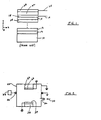
- the conventional thin-film piezoelectric filter depicted in FIG. 1 is formed on a substrate 10 made of silicon or other suitable material such as quartz or sapphire.
- the substrate 10 may comprise a standard twenty-centimeter-diameter wafer having a Y-direction thickness of about 600 micrometers ( ⁇ m).
- multiple filter devices are advantageously formed on the substrate 10 at the same time in a standard batch-fabrication process.
- the X and Z dimensions of the single depicted filter are each approximately 200-to-500 ⁇ m. The actual dimensions will depend on the particular design of the filter, as is well known.
- an acoustic Bragg reflector comprising alternating layers of high- and low-acoustic-impedance material is typically deposited on the top surface of the substrate 10 of FIG. 1.
- acoustic Bragg reflector comprising alternating layers of high- and low-acoustic-impedance material is typically deposited on the top surface of the substrate 10 of FIG. 1.
- four pairs of such layers each pair comprising a layer of silicon dioxide (SiO 2 ) and a layer of tantalum oxide (Ta 2 O 5 ), are so formed.
- the thickness of each such layer is selected to be equal to a quarter wavelength of the center frequency of the bandwidth of the indicated filter.
- Layers 12 (Ta 2 O 5 ), 13 (SiO 2 ) and 14 (Ta 2 O 5 ), 15(SiO 2 ) in FIG. 1 constitute two pairs of the layers of the noted acoustic reflector.
- a layer 18 constituting a bottom electrode of the herein-considered filter is formed overlying the aforedescribed multi-layer acoustic reflector.
- the layer 18 is made of a material that exhibits low electrical resistance and low acoustic loss.
- the layer 18 comprises aluminum (Al) or molybdenum (Mo) having, for example, a Y-direction thickness of about 1000 Angstrom units.
- An electrical lead 19 is shown connected to the bottom electrode layer 18.
- a layer 22 of a suitable piezoelectric material is formed on the electrode 18.
- a layer 22 of aluminum nitride (AlN) or zinc oxide (ZnO) having a Y-direction thickness of half the wavelength of the desired center frequency is deposited overlying the bottom electrode 18.
- an electrical lead 25 is connected to the top electrode layer 24.
- the electromechanical coupling constant of the piezoelectric layer 22 is a function of the crystalline orientation of the layer 22.
- the piezoelectric properties thereof are optimized if the layer is deposited such that its (002) crystalline axis is parallel to the depicted Y axis.
- a film of piezoelectric material having a predetermined crystalline orientation is deposited in a simple, robust and reliable manner that is consistently reproducible.
- Such a film exhibits good piezoelectric characteristics suitable for, for example, a variety of thin-film filter applications.
- FIG. 2 shows in simplified schematic form a specific illustrative apparatus of the type employed for depositing piezoelectric films in accordance with the invention.
- the apparatus comprises a reaction chamber 22 that is electrically connected to a point of reference potential such as ground.
- a substrate 24 whose top surface is to be coated with a thin piezoelectric film is shown mounted on a base member 26 within the chamber 22.
- a target 28 comprising a constituent of the material to be deposited on the substrate 24 is shown affixed to a member 30 in the chamber 22.
- gases are introduced into the reaction chamber 22 of FIG. 2 via inlet pipe 32, as indicated by arrow 34.
- the gases introduced into the chamber 22 comprise, for example, nitrogen (a constituent of the piezoelectric material to be deposited) and an inert gas such as argon.
- the target 28 is made of aluminum.
- the gases introduced into the chamber 22 of FIG. 2 are ionized. This is done by establishing a relatively high potential between the target 28 and the grounded chamber 22.
- this potential can be a constant direct-current (d-c) voltage.
- d-c direct-current
- a pulsed d-c voltage or an alternating-current voltage By way of example, assume that a constant d-c voltage is utilized for this purpose.
- the target 28 (made, for example, of aluminum) is maintained at a constant negative d-c potential of about 1000 volts relative to the chamber 22.
- a plasma comprising positively charged nitrogen and argon ions is thereby formed in the chamber. These ions are attracted to the negatively charged target 28.
- the nitrogen ions combine with aluminum to form a surface layer of AlN.
- the resulting AlN layer is impacted by argon ions. Particles of AlN are thereby dislodged from the target and propelled downward within the chamber 22.
- particles of a piezoelectric material for example, AlN
- a piezoelectric material for example, AlN
- r-f radio-frequency generator 38 which operates, for example, at a frequency of 13.56 megaHertz and supplies power in the range of 10-to-300 Watts.
- neutral particles of AlN dislodged from the target 28 are transformed in the chamber 22 into positive ions of AlN.
- these positive ions are attracted to and deposited on the surface of the substrate 24, which, for example, is connected to a negative d-c potential of about 100 volts.
- the attracted AlN ions are neutralized and form a layer of AlN.
- a layer of a piezoelectric material such as AlN deposited in the unique manner described above assumes a highly ordered crystalline orientation.
- AlN is deposited such that its (002) crystalline axis is highly parallel to the Y axis indicated in FIG. 1. Consequently, the deposited material exhibits good piezoelectric characteristics such as a coupling constant close to the theoretical maximum of 6.5% and an advantageous rocking curve characteristic.
- piezoelectric materials can be deposited in a prespecified oriented manner.
- the piezoelectric material to be deposited is first ionized and then electrostatically attracted to the substrate to be coated.
- a piezoelectric material such as ZnO can be deposited by following the techniques specified above.
- the target 28 of FIG. 2 is made of zinc, and the gases introduced into the chamber 22 via the inlet pipe 32 comprise oxygen (a constituent of the piezoelectric material to be deposited) and an inert gas such as argon.
- a layer of ZnO is thereby formed on the surface of the target 28.
- particles of this layer are dislodged by argon ions.
- dislodged particles are ionized by the aforementioned r-f field and deposited on the surface of the negatively charged substrate 24 in a highly oriented way.
- the resulting deposited film of ZnO exhibits a strong (002) crystalline orientation and good piezoelectric properties.
- the ionized piezoelectric material at a substrate that is specially prepared to further enhance the crystalline orientation that inherently results from depositing ionized material.
- the substrate comprises an aluminum electrode overlying a thin collimated layer of titanium nitride
- the aluminum electrode layer assumes a highly ordered orientation dictated by the titanium nitride.
- the subsequently deposited piezoelectric film assumes an even more highly ordered (002) crystalline orientation.
Landscapes
- Chemical & Material Sciences (AREA)
- Engineering & Computer Science (AREA)
- Materials Engineering (AREA)
- Organic Chemistry (AREA)
- Metallurgy (AREA)
- Mechanical Engineering (AREA)
- Chemical Kinetics & Catalysis (AREA)
- Crystallography & Structural Chemistry (AREA)
- Manufacturing & Machinery (AREA)
- Physics & Mathematics (AREA)
- Plasma & Fusion (AREA)
- Inorganic Chemistry (AREA)
- Physical Vapour Deposition (AREA)
- Piezo-Electric Or Mechanical Vibrators, Or Delay Or Filter Circuits (AREA)
Abstract
Description
Claims (10)
- A method for depositing a film of a piezoelectric material, said method comprising the steps ofionizing particles of a piezoelectric material that is to be deposited on the surface of a substrate,and electrostatically attracting said ionized particles to the surface of said substrate to form a film thereon.
- A method as in claim 1 wherein said steps occur in a reaction chamber into which are introduced an inert gas and a gas that comprises a constituent of said piezoelectric material.
- A method as in claim 2 wherein said introduced gases are ionized and electrostatically attracted to a target that comprises a constituent of said piezoelectric material.
- A method as in claim 3 wherein said constituent gas ions combine with the material of said target to form a piezoelectric material, and said inert gas ions dislodge particles of said piezoelectric material.
- A method as in claim 4 wherein said target comprises aluminum, said inert gas comprises argon, said constituent gas comprises nitrogen and said piezoelectric material comprises aluminum nitride.
- A method as in claim 5 wherein dislodged particles of aluminum nitride are ionized by an r-f electric field established within said chamber.
- A method as in claim 6 wherein the aluminum nitride piezoelectric film formed on the surface of said substrate exhibits an (002) crystalline orientation.
- A method as in claim 4 wherein said target comprises zinc, said inert gas comprises argon, said constituent gas comprises oxygen and said piezoelectric material comprises zinc oxide.
- A method as in claim 8 wherein dislodged particles of zinc oxide are ionized by an r-f electric field established within said chamber.
- A method as in claim 9 wherein the zinc oxide piezoelectric film formed on the surface of said substrate exhibits an (002) crystalline orientation.
Applications Claiming Priority (2)
| Application Number | Priority Date | Filing Date | Title |
|---|---|---|---|
| US09/363,758 US6153268A (en) | 1999-07-29 | 1999-07-29 | Method for producing oriented piezoelectric films |
| US363758 | 1999-07-29 |
Publications (2)
| Publication Number | Publication Date |
|---|---|
| EP1073197A2 true EP1073197A2 (en) | 2001-01-31 |
| EP1073197A3 EP1073197A3 (en) | 2002-02-06 |
Family
ID=23431600
Family Applications (1)
| Application Number | Title | Priority Date | Filing Date |
|---|---|---|---|
| EP00306073A Withdrawn EP1073197A3 (en) | 1999-07-29 | 2000-07-17 | Method for producing oriented piezoelectric films |
Country Status (8)
| Country | Link |
|---|---|
| US (1) | US6153268A (en) |
| EP (1) | EP1073197A3 (en) |
| JP (1) | JP2001098370A (en) |
| KR (1) | KR20010029980A (en) |
| CN (1) | CN1291825A (en) |
| AU (1) | AU4507200A (en) |
| BR (1) | BR0003014A (en) |
| CA (1) | CA2314302A1 (en) |
Families Citing this family (5)
| Publication number | Priority date | Publication date | Assignee | Title |
|---|---|---|---|---|
| JP2004200476A (en) * | 2002-12-19 | 2004-07-15 | Canon Inc | Method for manufacturing piezoelectric element |
| JP2006032485A (en) * | 2004-07-13 | 2006-02-02 | Brother Ind Ltd | Piezoelectric film forming method |
| US20140048013A1 (en) * | 2012-08-17 | 2014-02-20 | Intermolecular, Inc. | SEED LAYER FOR ZnO AND DOPED-ZnO THIN FILM NUCLEATION AND METHODS OF SEED LAYER DEPOSITION |
| US10483943B2 (en) | 2017-06-27 | 2019-11-19 | Globalfoundries Inc. | Artificially oriented piezoelectric film for integrated filters |
| GB2588941B (en) * | 2019-11-15 | 2022-08-17 | Dyson Technology Ltd | Method of depositing a material |
Family Cites Families (9)
| Publication number | Priority date | Publication date | Assignee | Title |
|---|---|---|---|---|
| US3988232A (en) * | 1974-06-25 | 1976-10-26 | Matsushita Electric Industrial Co., Ltd. | Method of making crystal films |
| US4309266A (en) * | 1980-07-18 | 1982-01-05 | Murata Manufacturing Co., Ltd. | Magnetron sputtering apparatus |
| JPS57118022A (en) * | 1981-01-12 | 1982-07-22 | Murata Mfg Co Ltd | Formation of zinc oxide film |
| JP3068901B2 (en) * | 1991-08-26 | 2000-07-24 | キヤノン株式会社 | Thin film preparation method |
| US5232571A (en) * | 1991-12-23 | 1993-08-03 | Iowa State University Research Foundation, Inc. | Aluminum nitride deposition using an AlN/Al sputter cycle technique |
| US5344676A (en) * | 1992-10-23 | 1994-09-06 | The Board Of Trustees Of The University Of Illinois | Method and apparatus for producing nanodrops and nanoparticles and thin film deposits therefrom |
| JPH06158274A (en) * | 1992-11-19 | 1994-06-07 | Seiko Instr Inc | Surface acoustic wave device and manufacturing method thereof |
| JPH1030179A (en) * | 1996-07-17 | 1998-02-03 | Fuji Electric Co Ltd | Method for producing zinc oxide film |
| US5948483A (en) * | 1997-03-25 | 1999-09-07 | The Board Of Trustees Of The University Of Illinois | Method and apparatus for producing thin film and nanoparticle deposits |
-
1999
- 1999-07-29 US US09/363,758 patent/US6153268A/en not_active Expired - Lifetime
-
2000
- 2000-07-04 AU AU45072/00A patent/AU4507200A/en not_active Abandoned
- 2000-07-17 EP EP00306073A patent/EP1073197A3/en not_active Withdrawn
- 2000-07-20 BR BR0003014-7A patent/BR0003014A/en not_active Application Discontinuation
- 2000-07-21 KR KR1020000041867A patent/KR20010029980A/en not_active Withdrawn
- 2000-07-21 CA CA002314302A patent/CA2314302A1/en not_active Abandoned
- 2000-07-27 JP JP2000226699A patent/JP2001098370A/en active Pending
- 2000-07-27 CN CN00121971A patent/CN1291825A/en active Pending
Also Published As
| Publication number | Publication date |
|---|---|
| AU4507200A (en) | 2001-02-01 |
| KR20010029980A (en) | 2001-04-16 |
| CN1291825A (en) | 2001-04-18 |
| US6153268A (en) | 2000-11-28 |
| CA2314302A1 (en) | 2001-01-29 |
| EP1073197A3 (en) | 2002-02-06 |
| BR0003014A (en) | 2001-03-13 |
| JP2001098370A (en) | 2001-04-10 |
Similar Documents
| Publication | Publication Date | Title |
|---|---|---|
| US5232571A (en) | Aluminum nitride deposition using an AlN/Al sputter cycle technique | |
| US6342134B1 (en) | Method for producing piezoelectric films with rotating magnetron sputtering system | |
| US6872289B2 (en) | Thin film fabrication method and thin film fabrication apparatus | |
| US5431799A (en) | Collimation hardware with RF bias rings to enhance sputter and/or substrate cavity ion generation efficiency | |
| US5401544A (en) | Method for manufacturing a surface acoustic wave device | |
| US10432162B2 (en) | Acoustic resonator including monolithic piezoelectric layer having opposite polarities | |
| US6475931B2 (en) | Method for producing devices having piezoelectric films | |
| US4309266A (en) | Magnetron sputtering apparatus | |
| US6312568B2 (en) | Two-step AIN-PVD for improved film properties | |
| JPS61218134A (en) | Device and method for forming thin film | |
| US8808513B2 (en) | Stress adjustment in reactive sputtering | |
| US6153268A (en) | Method for producing oriented piezoelectric films | |
| US20030068531A1 (en) | Film deposition method and film deposition system for depositing a halogen compound film, and magnesium fluoride film | |
| US3558351A (en) | Thin semiconductor films | |
| EP2660351B1 (en) | Radio frequency tuned substrate biased physical vapor deposition apparatus and method of operation | |
| JPH0649936B2 (en) | Bias spattering device | |
| JPS63233549A (en) | Thin film formation | |
| KR100399763B1 (en) | Method for manufacturing ZnO layer using sputtering deposition | |
| JP3515966B2 (en) | Method for manufacturing magneto-optical recording element | |
| JP3068901B2 (en) | Thin film preparation method | |
| EP1335037A2 (en) | Plasma cvd apparatus | |
| JPS63292625A (en) | Controlling method for plasma | |
| CN116155231A (en) | A kind of bulk acoustic wave resonator and preparation method thereof | |
| JPS61174633A (en) | Vacuum discharge treating device | |
| JPH0738373A (en) | Surface acoustic wave device and manufacturing method thereof |
Legal Events
| Date | Code | Title | Description |
|---|---|---|---|
| PUAI | Public reference made under article 153(3) epc to a published international application that has entered the european phase |
Free format text: ORIGINAL CODE: 0009012 |
|
| AK | Designated contracting states |
Kind code of ref document: A2 Designated state(s): AT BE CH CY DE DK ES FI FR GB GR IE IT LI LU MC NL PT SE |
|
| AX | Request for extension of the european patent |
Free format text: AL;LT;LV;MK;RO;SI |
|
| PUAL | Search report despatched |
Free format text: ORIGINAL CODE: 0009013 |
|
| AK | Designated contracting states |
Kind code of ref document: A3 Designated state(s): AT BE CH CY DE DK ES FI FR GB GR IE IT LI LU MC NL PT SE |
|
| AX | Request for extension of the european patent |
Free format text: AL;LT;LV;MK;RO;SI |
|
| AKX | Designation fees paid | ||
| REG | Reference to a national code |
Ref country code: DE Ref legal event code: 8566 |
|
| STAA | Information on the status of an ep patent application or granted ep patent |
Free format text: STATUS: THE APPLICATION IS DEEMED TO BE WITHDRAWN |
|
| 18D | Application deemed to be withdrawn |
Effective date: 20020807 |