EP0653776A1 - Plasma deposition systems for sputter deposition - Google Patents
Plasma deposition systems for sputter deposition Download PDFInfo
- Publication number
- EP0653776A1 EP0653776A1 EP94307308A EP94307308A EP0653776A1 EP 0653776 A1 EP0653776 A1 EP 0653776A1 EP 94307308 A EP94307308 A EP 94307308A EP 94307308 A EP94307308 A EP 94307308A EP 0653776 A1 EP0653776 A1 EP 0653776A1
- Authority
- EP
- European Patent Office
- Prior art keywords
- plasma
- antenna
- deposition system
- source
- target
- Prior art date
- Legal status (The legal status is an assumption and is not a legal conclusion. Google has not performed a legal analysis and makes no representation as to the accuracy of the status listed.)
- Withdrawn
Links
Images

Classifications
-
- H—ELECTRICITY
- H01—ELECTRIC ELEMENTS
- H01J—ELECTRIC DISCHARGE TUBES OR DISCHARGE LAMPS
- H01J37/00—Discharge tubes with provision for introducing objects or material to be exposed to the discharge, e.g. for the purpose of examination or processing thereof
- H01J37/32—Gas-filled discharge tubes
- H01J37/32009—Arrangements for generation of plasma specially adapted for examination or treatment of objects, e.g. plasma sources
- H01J37/32082—Radio frequency generated discharge
-
- H—ELECTRICITY
- H01—ELECTRIC ELEMENTS
- H01J—ELECTRIC DISCHARGE TUBES OR DISCHARGE LAMPS
- H01J37/00—Discharge tubes with provision for introducing objects or material to be exposed to the discharge, e.g. for the purpose of examination or processing thereof
- H01J37/32—Gas-filled discharge tubes
- H01J37/34—Gas-filled discharge tubes operating with cathodic sputtering
- H01J37/3402—Gas-filled discharge tubes operating with cathodic sputtering using supplementary magnetic fields
- H01J37/3405—Magnetron sputtering
-
- H—ELECTRICITY
- H01—ELECTRIC ELEMENTS
- H01J—ELECTRIC DISCHARGE TUBES OR DISCHARGE LAMPS
- H01J37/00—Discharge tubes with provision for introducing objects or material to be exposed to the discharge, e.g. for the purpose of examination or processing thereof
- H01J37/32—Gas-filled discharge tubes
- H01J37/34—Gas-filled discharge tubes operating with cathodic sputtering
- H01J37/3411—Constructional aspects of the reactor
- H01J37/3438—Electrodes other than cathode
-
- H—ELECTRICITY
- H01—ELECTRIC ELEMENTS
- H01J—ELECTRIC DISCHARGE TUBES OR DISCHARGE LAMPS
- H01J2237/00—Discharge tubes exposing object to beam, e.g. for analysis treatment, etching, imaging
- H01J2237/32—Processing objects by plasma generation
- H01J2237/33—Processing objects by plasma generation characterised by the type of processing
- H01J2237/332—Coating
- H01J2237/3322—Problems associated with coating
- H01J2237/3327—Coating high aspect ratio workpieces
Definitions
- the invention relates to physical vapor deposition equipment such as are used in the fabrication of integrated circuits and semiconductor devices.
- PVD Physical vapor deposition
- a target material e.g. Ti
- object e.g. a semiconductor wafer
- PVD Physical vapor deposition
- the process takes place in a vacuum chamber that contains an inert gas (e.g. argon).
- the plasma which is generated in the chamber between the negatively biased target and the wafer, ionizes the inert gas.
- the positively charged ionized gas atoms are pulled toward the negatively biased target and impact it with sufficient energy to expel (i.e., sputter) atoms of target material from the target.
- the sputtered atoms from the target are propelled toward the wafer where they form a layer of deposited material.
- the trajectories of the material coming off from the target during sputtering are distributed over a range of directions. Though typically most of the sputtered material is traveling in a direction that is normal to the target, a significant amount travels in other directions that diverge from the normal direction.
- the sputtered material traveling along the divergent directions tends to limit the definition that is obtainable at discontinuities on the wafer surface. More specifically, the material traveling along the non-normal trajectories deposits on the sidewalls of features such as thru holes and vias, thereby limiting how small one can make those features. For holes that are too small, the material deposited on the sidewalls eventually closes up the hole and prevents any further material from being deposited on the bottom of the hole.
- Collimation filters are used to filter out all sputtered material having a trajectory that diverges from the normal direction by more than a preselected angle.
- the collimation filter is placed between the target and the wafer. In general, it is a metal plate having a particular thickness with an array of holes passing through it.
- a honeycomb structure i.e., a pattern of hexagonal holes
- the holes have a specified aspect ratio, i.e., the ratio of their length to their diameter. The aspect ratio determines the degree of filtering which takes place. A higher aspect ratio produces a narrower angular filter (i.e., the preselected angle is smaller). A consequence of using a higher aspect ratio, however, is a significantly reduced throughput.
- picking the appropriate thickness and hole size for the collimation filter is simply a question of process optimization.
- the collimation filter reduces throughput by a factor of 5.
- users typically increase the operational power on the target. For example, rather than running at a 5 kW power level, the power is increased to about 20 kW.
- the increased power levels increase the rate of sputtering. They also, however, introduce other problems, e.g. increased temperature of the wafer and unwanted material interactions in the deposited layer.
- the invention is a plasma deposition system for sputter depositing material from a target onto a wafer.
- the system includes a chamber; a platform for holding the wafer during plasma processing; a source onto which the target is mounted; an equipotential conductive plane dividing the chamber into an upper cavity in which the target is located and a lower cavity in which the a wafer is located; and an upper antenna located inside the upper cavity and surrounding the plasma.
- the source generates a plasma in the chamber during operation.
- the equipotential conductive plane permits material sputtered from the target to pass into the lower cavity.
- the upper antenna couples RF power into the source-generated plasma.
- the plasma deposition system also includes a lower antenna located inside the lower cavity for generating a second plasma in the lower cavity.
- the equipotential plane is a collimation filter that is made of a refractory material (e.g. titanium).
- the invention is a plasma deposition system for sputter depositing material from a target onto a wafer.
- the system includes a chamber; a platform for holding the wafer during plasma processing; a source onto which the target is mounted; and an antenna located inside of the chamber and surrounding the plasma.
- the source generates a plasma in the chamber during operation and the antenna is for coupling RF power from an RF supply into the source-generated plasma.
- the user actually has quite limited control over the conditions under which the films are produced and thus the properties of the generated films. For example, it is generally not practical to lower the source power level (and thus the temperature) beyond a certain point because this also significantly reduces throughput. Though more desirable film properties may be achievable by operating at low DC power levels, high throughput is essential for production purposes. Thus, compromises must be made on what film properties are produced.
- the upper antenna permits the user to have much greater control over the plasma deposition process at throughputs that are acceptable for production purposes and to thereby access a wider range of film properties.
- the lower cavity antenna enables the user to exercise greater optimization control over the plasma deposition process.
- the nitrogen sticking coefficient strongly depends upon temperature as does the ability to react Ti with N2 to form TiN.
- these two reactions move in opposite directions with temperature.
- the sticking coefficient improves with decreasing temperatures, the reactivity of the reactive gas species decreases.
- a user can increase the reactivity of the N2 at lower temperatures where there is a better sticking coefficient without having to increase the power level of the source-generated plasma.
- the invention enables the user to run at a lower temperatures (and lower power levels) without sacrificing reactivity and thereby produce more stoichiometric films and films with different, possibly more desirable, properties.
- the lower cavity antenna also enables the user to more easily control the energy of the arriving species that is sputtered from the target. This, in turn, enables the user to have greater control over process optimization. For example, in aluminum planarization work using conventional deposition techniques, people have typically used DC or RF bias on the wafer to further stimulate the deposited atoms to move into the contacts. But this approach brought with it other problems. The arriving atoms, having much higher energy, altered the properties of the resulting film and tended to produce defects in the film. By using the ring antenna in the lower cavity to vary the impedance above the wafer, the user can change the film properties in an advantageous way without having to use high levels on the wafer to do so.
- the lower antenna couples it to the plasma and then lets the plasma potential enhance the bombardment energy.
- the user can employ very low bias on the wafer (e.g. 10 V) so that the energy of the arriving atoms is much lower and less likely to disrupt the film that is forming. This enables the user to have greater control over the density of the film and the surface states which affect the resulting barrier characteristics.
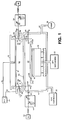
- a sputter deposition system includes a deposition chamber 10, a source assembly 12 on which a sputter target 14 is mounted, and a movable lower platform 16 holding a wafer 18 on which material sputtered from target 14 is deposited.
- the source assembly and the target mounted thereon are electrically isolated from the rest of the chamber by an insulator ring 20.
- the lower platform can be raised and lowered by a mechanical lift mechanism 22. After the wafer is placed on the platform, the lift mechanism raises the wafer until it contacts a clamping ring 24.
- the clamping ring has a central aperture 26 that is slightly smaller than the diameter of the wafer and it shields the platform from deposition material during processing.
- a vacuum pump 28 which is connected to the chamber througn a vacuum line 30, is used to evacuate the chamber at the beginning of a process run.
- Flow of inert gas (e.g. Ar) and reactive gases (e.g. N2) in and out of the chamber is controlled by gas control circuitry 32.
- Power for initiating and sustaining a plasma deposition process is supplied to the target by a DC voltage supply 34.
- the negative terminal of the DC supply is connected to the target through a line 36 and the positive terminal of the DC supply is connected to the wall of the chamber through another line 38.
- the source is a magnetron which includes a set of magnets (not shown) positioned behind the target material.
- the magnets increase the sputtering efficiency by preventing the electrons from rapidly escaping away from the face of the target and keeping them within a short distance of the target for a longer period of time so that they can thereby cause multiple ionizations of the inert gas (e.g. Ar).
- the magnets rotate around the back of the target in order to improve the uniformity of the erosion of the target during sputtering.
- a collimation filter 40 separates chamber 10 into an upper cavity 42 and a lower cavity 44.
- the collimation filter is connected to ground and thus forms a ground plane separating the two cavities.
- a cylindrical shield 46 that prevents material from being deposited on the walls of the chamber.
- the lower cavity also includes another cylindrical shield 48 which serves a similar purpose. Both shields are connected to ground potential.
- an upper ring antenna 50 couples RF power to the plasma generated by source 12.
- An RF generator 52 coupled to the upper ring antenna through an RF matching network 54 provides the RF power to the upper ring antenna.
- the electrical connection is made through a feed-through 56 in the wall of the chamber to one side of the upper ring antenna.
- the other side of the upper ring antenna is electrically connected to ground through another feed-through 58 in the chamber.
- a second ring antenna 60 couples RF power to the sputtered species passing through the collimation filter to the wafer.
- a second RF generator 62 coupled to lower ring antenna 60 through a second RF matching network 64 provides the RF power to the lower ring antenna.
- the electrical connection is made through a feed-through 66 in the wall of the chamber to one side of the lower ring antenna.
- the other side of the lower ring antenna is electrically connected to ground through another feed-through 68 in the chamber.
- the RF power supplied to the upper and lower ring antennas will be less than about 5 kW, though in some applications it may be desirable to use higher power levels (e.g. 20 kW). The precise power levels will depend upon the results that are desired and thus will vary from one application to the next.
- Each RF matching network creates a resonant circuit with its associated ring antenna so as to achieve high current in the antenna (i.e., efficient coupling of energy into the antenna). They include variable components that enable the user to tune them for optimum coupling to the plasma during a processing run. Since such tunable matching networks are well known to persons of ordinary skill in the art, they will not be described in greater detail here.
- the target size is about 13 inches.
- the target material may be any of a wide variety of materials including, for example, Ti, TiN, or W - materials which are typically used for producing ohmic contacts or device barriers.
- the spacing between the target and the wafer when the wafer is in a fully raised position is typically about 94 mm.
- the collimation filter is positioned approximately midway between the target and the wafer. It has a honeycomb structure, it is made of a refractory material such as titanium, it has a thickness of about 0.950 inch and the holes are about 0.625 inch in diameter.
- the upper and lower antennas are positioned at approximately the midpoints of in their respective cavities and are located around the inside periphery of the chamber.
- the upper and lower antennas provide a means by which the user can pump energy into the plasma and thereby dramatically affect the total production of ions.
- the upper and lower ring antennas are made of a conductive material (e.g. aluminum or copper) that is also resistant to the conditions existing in the plasma sputtering chamber. They may be single or multiple turn coils (e.g. 2-3 turns), the number of turns, of course, depending upon the frequency of the RF generators. In the described embodiment, RF frequencies within the range of 400 kHz to 40 MHz may be used.
- the plasma is generated by the DC voltage supply and the upper antenna provides a way to couple further energy into that plasma.
- the user can increase the number of inert gas ions that are available for sputtering the target at the power level determined by the DC voltage supply. That is, the upper antenna serves to lower the source impedance of the target.
- the upper antenna serves to lower the source impedance of the target.
- the user can increase throughput at a given power level and thereby compensate for the reduced throughput resulting from the collimation filter.
- the upper antenna since sputter distribution is dependent upon the source impedance, the upper antenna enables the user to control the shape of the sputter distribution.
- the upper antenna tends to ionize the material that is sputtered from the target, which tends to straighten the trajectories of the sputtered material and to further concentrate more of the plasma along the direction normal to the target.
- the improved sputtering efficiency achieved by the upper antenna may make it more practical to use sources other than a magnetron.
- the loss in efficiency attributable to some less efficient sources will be more than compensated by the beneficial effects of the upper antenna. Eliminating the magnetron has the added benefit of improving the erosion uniformity of the target.
- the lower cavity is separated from the upper cavity by a ground plane (i.e., the collimation filter), the plasma from the upper cavity will typically not penetrate into the lower cavity.
- the lower antenna and the RF generator driving it are used to strike and maintain a separate plasma in the lower cavity.
- the user can enhance the ionization of the reactive species (e.g. N2), which in turn will alter its reaction rate with the sputtered species.
- This capability may be particularly useful in, for example, coherent TiN deposition processes, in which it may be important to control the reactivity of the reactive gas species and to thereby produce films with different properties.
- the lower antenna can be used to optimize the bombardment energy to control the characteristics of the deposited material and the barrier characteristics.
- the upper and lower ring antennas are formed by continuous cylindrical plates or rings 80 and 82, respectively, rather than by coils.
- RF power is capacitively coupled into the plasma.
- the internal design of the chamber is similar to what was previously described.
- different RF matching circuits 84 and 86 are provided which are designed for efficiently coupling power into a capacitive load rather than an inductive load.
- the upper antenna can also be used in a deposition system by itself with no collimation filter or lower antenna. In that application, it would serve to control the target impedance and ionization efficiency as previously described.
- the described embodiment used a DC voltage supply as the power source, it could instead use an RF source or a hybrid DC voltage supply and RF power source. In addition, a DC bias could be applied to the wafer.
Abstract
The disclosure relates to a plasma deposition system for sputter depositing material from a target onto a wafer (18), the system including a chamber (10); a platform (16) for holding the wafer during plasma processing; a source (12) onto which the target (14) is mounted and for generating a plasma in the chamber during operation; an equipotential conductive plane (40) dividing the chamber into an upper cavity (42) in which the target is located, and a lower cavity (44) in which the wafer is located, the equipotential conductive plane permitting material sputtered from the target to pass therethrough; and an upper antenna (50) located inside the upper cavity and surrounding the plasma, the upper antenna for coupling RF power from an RF generator (52) into the source-generated plasma.
Description
- The invention relates to physical vapor deposition equipment such as are used in the fabrication of integrated circuits and semiconductor devices.
- Physical vapor deposition (PVD) is a process by which a target material (e.g. Ti) is deposited onto an object (e.g. a semiconductor wafer) by means of a plasma. The process takes place in a vacuum chamber that contains an inert gas (e.g. argon). The plasma, which is generated in the chamber between the negatively biased target and the wafer, ionizes the inert gas. The positively charged ionized gas atoms are pulled toward the negatively biased target and impact it with sufficient energy to expel (i.e., sputter) atoms of target material from the target. The sputtered atoms from the target are propelled toward the wafer where they form a layer of deposited material.
- The trajectories of the material coming off from the target during sputtering are distributed over a range of directions. Though typically most of the sputtered material is traveling in a direction that is normal to the target, a significant amount travels in other directions that diverge from the normal direction. The sputtered material traveling along the divergent directions tends to limit the definition that is obtainable at discontinuities on the wafer surface. More specifically, the material traveling along the non-normal trajectories deposits on the sidewalls of features such as thru holes and vias, thereby limiting how small one can make those features. For holes that are too small, the material deposited on the sidewalls eventually closes up the hole and prevents any further material from being deposited on the bottom of the hole.
- Collimation filters are used to filter out all sputtered material having a trajectory that diverges from the normal direction by more than a preselected angle. The collimation filter is placed between the target and the wafer. In general, it is a metal plate having a particular thickness with an array of holes passing through it. To maximize throughput, a honeycomb structure (i.e., a pattern of hexagonal holes) is used. The holes have a specified aspect ratio, i.e., the ratio of their length to their diameter. The aspect ratio determines the degree of filtering which takes place. A higher aspect ratio produces a narrower angular filter (i.e., the preselected angle is smaller). A consequence of using a higher aspect ratio, however, is a significantly reduced throughput. Thus, picking the appropriate thickness and hole size for the collimation filter is simply a question of process optimization.
- Nevertheless, for a typical filter design in a conventional system, only about 20% of the material will make it through the filter. The rest of the material, which represents sputtered material that has a trajectory that diverges from the normal direction by more than the preselected angle, deposits on the filter. In this example, the collimation filter reduces throughput by a factor of 5.
- To compensate for the reduced throughput, users typically increase the operational power on the target. For example, rather than running at a 5 kW power level, the power is increased to about 20 kW. The increased power levels increase the rate of sputtering. They also, however, introduce other problems, e.g. increased temperature of the wafer and unwanted material interactions in the deposited layer.
- It was discovered that much of the ionization in a plasma sputtering chamber occurs very close to the target, leaving a considerable amount of room for ionization enhancement throughout the rest of the plasma. It was also discovered that RF power can be effectively coupled into the DC generated plasma through a coil or ring antenna inside the chamber. The coupled RF power contributes to increasing ionization efficiency rather than causing a sputtering of the ring material.
- In general, in one aspect, the invention is a plasma deposition system for sputter depositing material from a target onto a wafer. The system includes a chamber; a platform for holding the wafer during plasma processing; a source onto which the target is mounted; an equipotential conductive plane dividing the chamber into an upper cavity in which the target is located and a lower cavity in which the a wafer is located; and an upper antenna located inside the upper cavity and surrounding the plasma. The source generates a plasma in the chamber during operation. The equipotential conductive plane permits material sputtered from the target to pass into the lower cavity. And the upper antenna couples RF power into the source-generated plasma.
- In preferred embodiments, the plasma deposition system also includes a lower antenna located inside the lower cavity for generating a second plasma in the lower cavity. Also, the equipotential plane is a collimation filter that is made of a refractory material (e.g. titanium).
- In general, in another aspect, the invention is a plasma deposition system for sputter depositing material from a target onto a wafer. The system includes a chamber; a platform for holding the wafer during plasma processing; a source onto which the target is mounted; and an antenna located inside of the chamber and surrounding the plasma. The source generates a plasma in the chamber during operation and the antenna is for coupling RF power from an RF supply into the source-generated plasma.
- With conventional plasma deposition techniques, the user actually has quite limited control over the conditions under which the films are produced and thus the properties of the generated films. For example, it is generally not practical to lower the source power level (and thus the temperature) beyond a certain point because this also significantly reduces throughput. Though more desirable film properties may be achievable by operating at low DC power levels, high throughput is essential for production purposes. Thus, compromises must be made on what film properties are produced. The upper antenna permits the user to have much greater control over the plasma deposition process at throughputs that are acceptable for production purposes and to thereby access a wider range of film properties.
- The lower cavity antenna enables the user to exercise greater optimization control over the plasma deposition process. For example, the nitrogen sticking coefficient strongly depends upon temperature as does the ability to react Ti with N₂ to form TiN. However, these two reactions move in opposite directions with temperature. While the sticking coefficient improves with decreasing temperatures, the reactivity of the reactive gas species decreases. In a conventional system, there is generally an optimum process temperature at which one achieves the best reactivity while still maintaining acceptable sticking coefficient. Thus, when using conventional plasma deposition techniques, one must run at the appropriate power level which achieves the optimum temperature. With the invention, however, a user can increase the reactivity of the N₂ at lower temperatures where there is a better sticking coefficient without having to increase the power level of the source-generated plasma. Thus, the invention enables the user to run at a lower temperatures (and lower power levels) without sacrificing reactivity and thereby produce more stoichiometric films and films with different, possibly more desirable, properties.
- The lower cavity antenna also enables the user to more easily control the energy of the arriving species that is sputtered from the target. This, in turn, enables the user to have greater control over process optimization. For example, in aluminum planarization work using conventional deposition techniques, people have typically used DC or RF bias on the wafer to further stimulate the deposited atoms to move into the contacts. But this approach brought with it other problems. The arriving atoms, having much higher energy, altered the properties of the resulting film and tended to produce defects in the film. By using the ring antenna in the lower cavity to vary the impedance above the wafer, the user can change the film properties in an advantageous way without having to use high levels on the wafer to do so. Rather than coupling RF or DC power to the wafer, the lower antenna couples it to the plasma and then lets the plasma potential enhance the bombardment energy. Thus, the user can employ very low bias on the wafer (e.g. 10 V) so that the energy of the arriving atoms is much lower and less likely to disrupt the film that is forming. This enables the user to have greater control over the density of the film and the surface states which affect the resulting barrier characteristics.
- Other advantages and features will become apparent from the following description of a preferred embodiment reference being made to the accompanying drawings, in which:
- Fig. 1 shows a sputter deposition chamber including a collimation filter as well as upper and lower cavity RF bias ring antennas that both inductively couple to the plasma within the chamber; and
- Fig. 2 shows an alternative embodiment using upper and lower chamber RF bias ring antennas that capacitively couple to the plasma within the chamber.
- Referring to Fig. 1, a sputter deposition system includes a
deposition chamber 10, asource assembly 12 on which asputter target 14 is mounted, and a movablelower platform 16 holding awafer 18 on which material sputtered fromtarget 14 is deposited. The source assembly and the target mounted thereon are electrically isolated from the rest of the chamber by aninsulator ring 20. The lower platform can be raised and lowered by amechanical lift mechanism 22. After the wafer is placed on the platform, the lift mechanism raises the wafer until it contacts aclamping ring 24. The clamping ring has acentral aperture 26 that is slightly smaller than the diameter of the wafer and it shields the platform from deposition material during processing. - A
vacuum pump 28, which is connected to the chamber througn avacuum line 30, is used to evacuate the chamber at the beginning of a process run. Flow of inert gas (e.g. Ar) and reactive gases (e.g. N₂) in and out of the chamber is controlled bygas control circuitry 32. Power for initiating and sustaining a plasma deposition process is supplied to the target by aDC voltage supply 34. The negative terminal of the DC supply is connected to the target through aline 36 and the positive terminal of the DC supply is connected to the wall of the chamber through anotherline 38. - In the described embodiment, the source is a magnetron which includes a set of magnets (not shown) positioned behind the target material. The magnets increase the sputtering efficiency by preventing the electrons from rapidly escaping away from the face of the target and keeping them within a short distance of the target for a longer period of time so that they can thereby cause multiple ionizations of the inert gas (e.g. Ar). In such a source, the magnets rotate around the back of the target in order to improve the uniformity of the erosion of the target during sputtering.
- A
collimation filter 40separates chamber 10 into anupper cavity 42 and alower cavity 44. The collimation filter is connected to ground and thus forms a ground plane separating the two cavities. Within the upper cavity and around its inside perimeter there is acylindrical shield 46 that prevents material from being deposited on the walls of the chamber. Likewise, the lower cavity also includes anothercylindrical shield 48 which serves a similar purpose. Both shields are connected to ground potential. - Inside the upper cavity, an
upper ring antenna 50 couples RF power to the plasma generated bysource 12. AnRF generator 52 coupled to the upper ring antenna through anRF matching network 54 provides the RF power to the upper ring antenna. The electrical connection is made through a feed-through 56 in the wall of the chamber to one side of the upper ring antenna. The other side of the upper ring antenna is electrically connected to ground through another feed-through 58 in the chamber. - Inside the lower cavity, a
second ring antenna 60 couples RF power to the sputtered species passing through the collimation filter to the wafer. Asecond RF generator 62 coupled tolower ring antenna 60 through a secondRF matching network 64 provides the RF power to the lower ring antenna. As with the upper ring antenna, the electrical connection is made through a feed-through 66 in the wall of the chamber to one side of the lower ring antenna. The other side of the lower ring antenna is electrically connected to ground through another feed-through 68 in the chamber. - Typically, the RF power supplied to the upper and lower ring antennas will be less than about 5 kW, though in some applications it may be desirable to use higher power levels (e.g. 20 kW). The precise power levels will depend upon the results that are desired and thus will vary from one application to the next.
- Each RF matching network creates a resonant circuit with its associated ring antenna so as to achieve high current in the antenna (i.e., efficient coupling of energy into the antenna). They include variable components that enable the user to tune them for optimum coupling to the plasma during a processing run. Since such tunable matching networks are well known to persons of ordinary skill in the art, they will not be described in greater detail here.
- In the described embodiment, which processes 8 inch wafers, the target size is about 13 inches. The target material may be any of a wide variety of materials including, for example, Ti, TiN, or W - materials which are typically used for producing ohmic contacts or device barriers. The spacing between the target and the wafer when the wafer is in a fully raised position is typically about 94 mm. The collimation filter is positioned approximately midway between the target and the wafer. It has a honeycomb structure, it is made of a refractory material such as titanium, it has a thickness of about 0.950 inch and the holes are about 0.625 inch in diameter. The upper and lower antennas are positioned at approximately the midpoints of in their respective cavities and are located around the inside periphery of the chamber.
- The upper and lower antennas provide a means by which the user can pump energy into the plasma and thereby dramatically affect the total production of ions. The upper and lower ring antennas are made of a conductive material (e.g. aluminum or copper) that is also resistant to the conditions existing in the plasma sputtering chamber. They may be single or multiple turn coils (e.g. 2-3 turns), the number of turns, of course, depending upon the frequency of the RF generators. In the described embodiment, RF frequencies within the range of 400 kHz to 40 MHz may be used.
- In the upper cavity, the plasma is generated by the DC voltage supply and the upper antenna provides a way to couple further energy into that plasma. By pumping further energy into the plasma, the user can increase the number of inert gas ions that are available for sputtering the target at the power level determined by the DC voltage supply. That is, the upper antenna serves to lower the source impedance of the target. Thus, with the aid of the upper antenna, the user can increase throughput at a given power level and thereby compensate for the reduced throughput resulting from the collimation filter. Also, since sputter distribution is dependent upon the source impedance, the upper antenna enables the user to control the shape of the sputter distribution. In addition, the upper antenna tends to ionize the material that is sputtered from the target, which tends to straighten the trajectories of the sputtered material and to further concentrate more of the plasma along the direction normal to the target. Thus, it becomes possible to reduce the amount of material that is deposited on the filter and further increase throughput.
- It should be noted that the improved sputtering efficiency achieved by the upper antenna may make it more practical to use sources other than a magnetron. The loss in efficiency attributable to some less efficient sources will be more than compensated by the beneficial effects of the upper antenna. Eliminating the magnetron has the added benefit of improving the erosion uniformity of the target.
- Since the lower cavity is separated from the upper cavity by a ground plane (i.e., the collimation filter), the plasma from the upper cavity will typically not penetrate into the lower cavity. Thus, the lower antenna and the RF generator driving it are used to strike and maintain a separate plasma in the lower cavity. Through the second plasma generated in the lower cavity, the user can enhance the ionization of the reactive species (e.g. N₂), which in turn will alter its reaction rate with the sputtered species. This capability may be particularly useful in, for example, coherent TiN deposition processes, in which it may be important to control the reactivity of the reactive gas species and to thereby produce films with different properties.
- Note that turning on the RF power to the lower antenna does not affect the sputter rate of the target but it does increase the bombardment energy and ionization of the sputtered species onto the wafer. Thus, the lower antenna can be used to optimize the bombardment energy to control the characteristics of the deposited material and the barrier characteristics.
- Referring to Fig. 2, in a capacitively coupled system, the upper and lower ring antennas are formed by continuous cylindrical plates or rings 80 and 82, respectively, rather than by coils. Through the cylindrical plates, RF power is capacitively coupled into the plasma. In all other respects, however, the internal design of the chamber is similar to what was previously described. Of course, different
RF matching circuits Helmholtz coils 90 that are located outside of and surround the chamber, as shown diagrammatically in the figure. - Other embodiments are within the following claims. For example, the upper antenna can also be used in a deposition system by itself with no collimation filter or lower antenna. In that application, it would serve to control the target impedance and ionization efficiency as previously described. Also, though the described embodiment used a DC voltage supply as the power source, it could instead use an RF source or a hybrid DC voltage supply and RF power source. In addition, a DC bias could be applied to the wafer.
Claims (20)
- A plasma deposition system for sputter depositing material from a target onto a wafer, said system comprising:
a chamber;
a platform for holding the wafer during plasma processing;
a source onto which the target is mounted, said source generating a plasma in said chamber during operation;
an equipotential conductive plane dividing said chamber into an upper cavity in which the target is located and a lower cavity in which the a wafer is located, said equipotential conductive plane permitting material sputtered from said target to pass therethrough; and
an upper antenna located inside the upper cavity and surrounding the plasma, said upper antenna for coupling RF power into the source-generated plasma. - The plasma deposition system of claim 1 further comprising a lower antenna located inside the lower cavity and for generating a second plasma in the lower cavity.
- The plasma deposition system of claim 1 wherein said equipotential plane is a collimation filter.
- The plasma deposition system of claim 3 wherein said collimation filter is made of a refractory material.
- The plasma deposition system of claim 4 wherein said collimation filter is made of titanium.
- The plasma deposition system of claim 2 further comprising a first matching circuit connected to said upper antenna and a first RF generator providing RF power to said upper antenna through said first matching circuit.
- The plasma deposition system of claim 6 further comprising a second matching circuit connected to said lower antenna and a second RF generator providing RF power to said lower antenna through said second matching circuit.
- The plasma deposition system of claim 1 wherein said upper antenna is a coil through which RF power is inductively coupled into said source-generated plasma.
- The plasma deposition system of claim 8 wherein said upper cavity coil has multiple turns.
- The plasma deposition system of claim 2 wherein said lower antenna is a coil through which RF power is inductively coupled into said second plasma.
- The plasma deposition system of claim 10 wherein said lower cavity coil has multiple turns.
- The plasma deposition system of claim 1 wherein said upper antenna is a cylindrical plate through which RF power is capacitively coupled into said source-generated plasma.
- The plasma deposition system of claim 2 wherein said lower antenna is a cylindrical plate through which RF power is capacitively coupled into said second plasma.
- The plasma deposition system of claim 1 further comprising a DC power supply connected to said source, said DC power supply generating said source-generated plasma.
- A plasma deposition system for sputter depositing material from a target onto a wafer, said system comprising:
a chamber;
a platform for holding the wafer during plasma processing;
a source onto which the target is mounted, said source generating a plasma in said chamber during operation;
an equipotential conductive plane dividing said chamber into an upper cavity in which the target is located and a lower cavity in which the a wafer is located, said equipotential conductive plane permitting material sputtered from said target to pass therethrough;
an upper antenna located inside the upper cavity and surrounding the plasma, said upper antenna for coupling RF power into the source-generated plasma.
a first matching circuit connected to said upper antenna;
a first RF generator providing RF power to said upper antenna through said first matching circuit;
a lower antenna located inside the lower cavity and for generating a second plasma in the lower cavity.
a second matching circuit connected to said lower antenna; and
a second RF generator providing RF power to said lower antenna through said second matching circuit. - A plasma deposition system for sputter depositing material from a target onto a wafer, said system comprising:
a chamber;
a platform for holding the wafer during plasma processing;
a source onto which the target is mounted, said source generating a plasma in said chamber during operation; and
an antenna located inside of the chamber and surrounding the plasma, said antenna for coupling RF power from an RF supply into the source-generated plasma. - The plasma deposition system of claim 16 further comprising a first matching circuit connected to said upper antenna and a first RF generator providing RF power to said upper antenna through said first matching circuit.
- The plasma deposition system of claim 17 wherein said upper antenna is a coil through which RF power is inductively coupled into said source-generated plasma.
- The plasma deposition system of claim 18 wherein said upper cavity coil has multiple turns.
- The plasma deposition system of claim 17 further comprising a DC power supply connected to said source, said DC power supply generating said source-generated plasma.
Applications Claiming Priority (2)
| Application Number | Priority Date | Filing Date | Title |
|---|---|---|---|
| US145744 | 1993-10-29 | ||
| US08/145,744 US5431799A (en) | 1993-10-29 | 1993-10-29 | Collimation hardware with RF bias rings to enhance sputter and/or substrate cavity ion generation efficiency |
Publications (1)
| Publication Number | Publication Date |
|---|---|
| EP0653776A1 true EP0653776A1 (en) | 1995-05-17 |
Family
ID=22514337
Family Applications (1)
| Application Number | Title | Priority Date | Filing Date |
|---|---|---|---|
| EP94307308A Withdrawn EP0653776A1 (en) | 1993-10-29 | 1994-10-05 | Plasma deposition systems for sputter deposition |
Country Status (3)
| Country | Link |
|---|---|
| US (1) | US5431799A (en) |
| EP (1) | EP0653776A1 (en) |
| JP (1) | JPH07188917A (en) |
Cited By (17)
| Publication number | Priority date | Publication date | Assignee | Title |
|---|---|---|---|---|
| WO1998052207A2 (en) * | 1997-05-16 | 1998-11-19 | Applied Materials, Inc. | Central coil design for ionized metal plasma deposition |
| EP0908531A2 (en) * | 1997-10-08 | 1999-04-14 | Canon Kabushiki Kaisha | Apparatus and method for forming a thin film of a compound |
| FR2784906A1 (en) * | 1998-09-28 | 2000-04-28 | Cit Alcatel | PLASMA REACTOR FOR THE SPRAYING OF METAL AND DIELECTRIC FILMS |
| US6146508A (en) * | 1998-04-22 | 2000-11-14 | Applied Materials, Inc. | Sputtering method and apparatus with small diameter RF coil |
| US6210539B1 (en) | 1997-05-14 | 2001-04-03 | Applied Materials, Inc. | Method and apparatus for producing a uniform density plasma above a substrate |
| US6361661B2 (en) | 1997-05-16 | 2002-03-26 | Applies Materials, Inc. | Hybrid coil design for ionized deposition |
| US6506287B1 (en) | 1998-03-16 | 2003-01-14 | Applied Materials, Inc. | Overlap design of one-turn coil |
| WO2003043052A1 (en) * | 2001-11-14 | 2003-05-22 | Applied Materials, Inc. | Magnet array in conjunction with rotating magnetron for plasma sputtering |
| US6660134B1 (en) | 1998-07-10 | 2003-12-09 | Applied Materials, Inc. | Feedthrough overlap coil |
| US7041201B2 (en) | 2001-11-14 | 2006-05-09 | Applied Materials, Inc. | Sidewall magnet improving uniformity of inductively coupled plasma and shields used therewith |
| EP2345750A1 (en) * | 2008-08-28 | 2011-07-20 | EMD Corporation | Thin film-forming sputtering device |
| US8398832B2 (en) * | 1996-05-09 | 2013-03-19 | Applied Materials Inc. | Coils for generating a plasma and for sputtering |
| US8668816B2 (en) | 1999-10-08 | 2014-03-11 | Applied Materials Inc. | Self-ionized and inductively-coupled plasma for sputtering and resputtering |
| CN103849848A (en) * | 2012-11-28 | 2014-06-11 | 北京北方微电子基地设备工艺研究中心有限责任公司 | Physical vapor deposition apparatus |
| EP2752501A1 (en) * | 2011-08-30 | 2014-07-09 | EMD Corporation | Sputtering thin film forming apparatus |
| US9062372B2 (en) | 2002-08-01 | 2015-06-23 | Applied Materials, Inc. | Self-ionized and capacitively-coupled plasma for sputtering and resputtering |
| US10047430B2 (en) | 1999-10-08 | 2018-08-14 | Applied Materials, Inc. | Self-ionized and inductively-coupled plasma for sputtering and resputtering |
Families Citing this family (69)
| Publication number | Priority date | Publication date | Assignee | Title |
|---|---|---|---|---|
| JP2671835B2 (en) * | 1994-10-20 | 1997-11-05 | 日本電気株式会社 | Sputtering apparatus and method for manufacturing semiconductor device using the apparatus |
| EP0735577A3 (en) * | 1994-12-14 | 1997-04-02 | Applied Materials Inc | Deposition process and apparatus therefor |
| US6224724B1 (en) | 1995-02-23 | 2001-05-01 | Tokyo Electron Limited | Physical vapor processing of a surface with non-uniformity compensation |
| US6132564A (en) * | 1997-11-17 | 2000-10-17 | Tokyo Electron Limited | In-situ pre-metallization clean and metallization of semiconductor wafers |
| JP3122601B2 (en) * | 1995-06-15 | 2001-01-09 | 東京エレクトロン株式会社 | Plasma film forming method and apparatus therefor |
| US5653811A (en) | 1995-07-19 | 1997-08-05 | Chan; Chung | System for the plasma treatment of large area substrates |
| US6264812B1 (en) * | 1995-11-15 | 2001-07-24 | Applied Materials, Inc. | Method and apparatus for generating a plasma |
| US5705042A (en) * | 1996-01-29 | 1998-01-06 | Micron Technology, Inc. | Electrically isolated collimator and method |
| US5985102A (en) * | 1996-01-29 | 1999-11-16 | Micron Technology, Inc. | Kit for electrically isolating collimator of PVD chamber, chamber so modified, and method of using |
| US6340417B1 (en) * | 1996-03-14 | 2002-01-22 | Advanced Micro Devices, Inc. | Reactor and method for ionized metal deposition |
| US6827824B1 (en) * | 1996-04-12 | 2004-12-07 | Micron Technology, Inc. | Enhanced collimated deposition |
| US6368469B1 (en) * | 1996-05-09 | 2002-04-09 | Applied Materials, Inc. | Coils for generating a plasma and for sputtering |
| US5846883A (en) * | 1996-07-10 | 1998-12-08 | Cvc, Inc. | Method for multi-zone high-density inductively-coupled plasma generation |
| US5707498A (en) * | 1996-07-12 | 1998-01-13 | Applied Materials, Inc. | Avoiding contamination from induction coil in ionized sputtering |
| US6254737B1 (en) * | 1996-10-08 | 2001-07-03 | Applied Materials, Inc. | Active shield for generating a plasma for sputtering |
| US5961793A (en) * | 1996-10-31 | 1999-10-05 | Applied Materials, Inc. | Method of reducing generation of particulate matter in a sputtering chamber |
| TW358964B (en) * | 1996-11-21 | 1999-05-21 | Applied Materials Inc | Method and apparatus for improving sidewall coverage during sputtering in a chamber having an inductively coupled plasma |
| US6254747B1 (en) * | 1996-12-25 | 2001-07-03 | Nihon Shinku Gijutsu Kabushiki Kaisha | Magnetron sputtering source enclosed by a mirror-finished metallic cover |
| US6451179B1 (en) | 1997-01-30 | 2002-09-17 | Applied Materials, Inc. | Method and apparatus for enhancing sidewall coverage during sputtering in a chamber having an inductively coupled plasma |
| JPH10251849A (en) * | 1997-03-07 | 1998-09-22 | Tadahiro Omi | Sputtering device |
| US5911113A (en) * | 1997-03-18 | 1999-06-08 | Applied Materials, Inc. | Silicon-doped titanium wetting layer for aluminum plug |
| JP3846970B2 (en) * | 1997-04-14 | 2006-11-15 | キヤノンアネルバ株式会社 | Ionization sputtering equipment |
| US5948215A (en) * | 1997-04-21 | 1999-09-07 | Tokyo Electron Limited | Method and apparatus for ionized sputtering |
| US5800688A (en) * | 1997-04-21 | 1998-09-01 | Tokyo Electron Limited | Apparatus for ionized sputtering |
| US6103070A (en) * | 1997-05-14 | 2000-08-15 | Applied Materials, Inc. | Powered shield source for high density plasma |
| US5830330A (en) * | 1997-05-22 | 1998-11-03 | Tokyo Electron Limited | Method and apparatus for low pressure sputtering |
| US6083363A (en) * | 1997-07-02 | 2000-07-04 | Tokyo Electron Limited | Apparatus and method for uniform, low-damage anisotropic plasma processing |
| US6042700A (en) * | 1997-09-15 | 2000-03-28 | Applied Materials, Inc. | Adjustment of deposition uniformity in an inductively coupled plasma source |
| US6023038A (en) * | 1997-09-16 | 2000-02-08 | Applied Materials, Inc. | Resistive heating of powered coil to reduce transient heating/start up effects multiple loadlock system |
| US6136165A (en) * | 1997-11-26 | 2000-10-24 | Cvc Products, Inc. | Apparatus for inductively-coupled-plasma-enhanced ionized physical-vapor deposition |
| DE19755837A1 (en) * | 1997-12-16 | 1999-06-17 | Leybold Ag | Sputtering unit employs an electrically isolated substrate edge mask |
| US6269765B1 (en) * | 1998-02-11 | 2001-08-07 | Silicon Genesis Corporation | Collection devices for plasma immersion ion implantation |
| US6274459B1 (en) | 1998-02-17 | 2001-08-14 | Silicon Genesis Corporation | Method for non mass selected ion implant profile control |
| US6287436B1 (en) | 1998-02-27 | 2001-09-11 | Innovent, Inc. | Brazed honeycomb collimator |
| US6093966A (en) * | 1998-03-20 | 2000-07-25 | Motorola, Inc. | Semiconductor device with a copper barrier layer and formation thereof |
| US6162332A (en) * | 1998-05-07 | 2000-12-19 | Taiwan Semiconductor Manufacturing Company, Ltd. | Method and apparatus for preventing arcing in sputter chamber |
| WO2000003055A1 (en) * | 1998-07-13 | 2000-01-20 | Tokyo Electron Arizona, Inc. | Shield for ionized physical vapor deposition apparatus |
| TW434636B (en) | 1998-07-13 | 2001-05-16 | Applied Komatsu Technology Inc | RF matching network with distributed outputs |
| US6057244A (en) * | 1998-07-31 | 2000-05-02 | Applied Materials, Inc. | Method for improved sputter etch processing |
| US6592728B1 (en) * | 1998-08-04 | 2003-07-15 | Veeco-Cvc, Inc. | Dual collimated deposition apparatus and method of use |
| US6231725B1 (en) | 1998-08-04 | 2001-05-15 | Applied Materials, Inc. | Apparatus for sputtering material onto a workpiece with the aid of a plasma |
| JP3187011B2 (en) * | 1998-08-31 | 2001-07-11 | 日本電気株式会社 | Method for manufacturing semiconductor device |
| US6238528B1 (en) | 1998-10-13 | 2001-05-29 | Applied Materials, Inc. | Plasma density modulator for improved plasma density uniformity and thickness uniformity in an ionized metal plasma source |
| GB2342927B (en) * | 1998-10-23 | 2003-05-07 | Trikon Holdings Ltd | Apparatus and methods for sputtering |
| US6579421B1 (en) * | 1999-01-07 | 2003-06-17 | Applied Materials, Inc. | Transverse magnetic field for ionized sputter deposition |
| JP2000226655A (en) * | 1999-02-02 | 2000-08-15 | Matsushita Electric Ind Co Ltd | Sputtering device |
| US6458723B1 (en) | 1999-06-24 | 2002-10-01 | Silicon Genesis Corporation | High temperature implant apparatus |
| US6409890B1 (en) * | 1999-07-27 | 2002-06-25 | Applied Materials, Inc. | Method and apparatus for forming a uniform layer on a workpiece during sputtering |
| US6143140A (en) * | 1999-08-16 | 2000-11-07 | Applied Materials, Inc. | Method and apparatus to improve the side wall and bottom coverage in IMP process by using magnetic field |
| US6168696B1 (en) | 1999-09-01 | 2001-01-02 | Micron Technology, Inc. | Non-knurled induction coil for ionized metal deposition, sputtering apparatus including same, and method of constructing the apparatus |
| US6458251B1 (en) * | 1999-11-16 | 2002-10-01 | Applied Materials, Inc. | Pressure modulation method to obtain improved step coverage of seed layer |
| US6312568B2 (en) | 1999-12-07 | 2001-11-06 | Applied Materials, Inc. | Two-step AIN-PVD for improved film properties |
| US6699375B1 (en) * | 2000-06-29 | 2004-03-02 | Applied Materials, Inc. | Method of extending process kit consumable recycling life |
| US6471830B1 (en) | 2000-10-03 | 2002-10-29 | Veeco/Cvc, Inc. | Inductively-coupled-plasma ionized physical-vapor deposition apparatus, method and system |
| US6764940B1 (en) | 2001-03-13 | 2004-07-20 | Novellus Systems, Inc. | Method for depositing a diffusion barrier for copper interconnect applications |
| US7298091B2 (en) * | 2002-02-01 | 2007-11-20 | The Regents Of The University Of California | Matching network for RF plasma source |
| US8298933B2 (en) | 2003-04-11 | 2012-10-30 | Novellus Systems, Inc. | Conformal films on semiconductor substrates |
| US7842605B1 (en) | 2003-04-11 | 2010-11-30 | Novellus Systems, Inc. | Atomic layer profiling of diffusion barrier and metal seed layers |
| US20050098427A1 (en) * | 2003-11-11 | 2005-05-12 | Taiwan Semiconductor Manufacturing Co., Ltd. | RF coil design for improved film uniformity of an ion metal plasma source |
| US7695590B2 (en) | 2004-03-26 | 2010-04-13 | Applied Materials, Inc. | Chemical vapor deposition plasma reactor having plural ion shower grids |
| US20050211547A1 (en) * | 2004-03-26 | 2005-09-29 | Applied Materials, Inc. | Reactive sputter deposition plasma reactor and process using plural ion shower grids |
| US7767561B2 (en) | 2004-07-20 | 2010-08-03 | Applied Materials, Inc. | Plasma immersion ion implantation reactor having an ion shower grid |
| US8058156B2 (en) | 2004-07-20 | 2011-11-15 | Applied Materials, Inc. | Plasma immersion ion implantation reactor having multiple ion shower grids |
| US7456095B2 (en) * | 2005-10-03 | 2008-11-25 | International Business Machines Corporation | Method and apparatus for forming nickel silicide with low defect density in FET devices |
| US7510634B1 (en) | 2006-11-10 | 2009-03-31 | Novellus Systems, Inc. | Apparatus and methods for deposition and/or etch selectivity |
| JP2011524471A (en) * | 2008-06-17 | 2011-09-01 | アプライド マテリアルズ インコーポレイテッド | Apparatus and method for uniform deposition |
| US10692706B2 (en) * | 2013-03-12 | 2020-06-23 | Applied Materials, Inc. | Methods and apparatus for reducing sputtering of a grounded shield in a process chamber |
| EP3920210B1 (en) | 2015-10-27 | 2023-05-31 | Applied Materials, Inc. | Biasable flux optimizer/collimator for pvd sputter chamber |
| CN113474483A (en) * | 2019-02-07 | 2021-10-01 | 朗姆研究公司 | Substrate processing capable of temporally and/or spatially modulating one or more plasmas |
Citations (3)
| Publication number | Priority date | Publication date | Assignee | Title |
|---|---|---|---|---|
| EP0313750A1 (en) * | 1987-10-29 | 1989-05-03 | International Business Machines Corporation | Magnetron sputter etching/deposition system |
| US4931158A (en) * | 1988-03-22 | 1990-06-05 | The Regents Of The Univ. Of Calif. | Deposition of films onto large area substrates using modified reactive magnetron sputtering |
| US5178739A (en) * | 1990-10-31 | 1993-01-12 | International Business Machines Corporation | Apparatus for depositing material into high aspect ratio holes |
Family Cites Families (10)
| Publication number | Priority date | Publication date | Assignee | Title |
|---|---|---|---|---|
| US3649502A (en) * | 1969-08-14 | 1972-03-14 | Precision Instr Co | Apparatus for supported discharge sputter-coating of a substrate |
| JPS61190070A (en) * | 1985-02-20 | 1986-08-23 | Hitachi Ltd | Sputter device |
| JP2515731B2 (en) * | 1985-10-25 | 1996-07-10 | 株式会社日立製作所 | Thin film forming apparatus and thin film forming method |
| US4668338A (en) * | 1985-12-30 | 1987-05-26 | Applied Materials, Inc. | Magnetron-enhanced plasma etching process |
| US4962063A (en) * | 1988-11-10 | 1990-10-09 | Applied Materials, Inc. | Multistep planarized chemical vapor deposition process with the use of low melting inorganic material for flowing while depositing |
| US5108569A (en) * | 1989-11-30 | 1992-04-28 | Applied Materials, Inc. | Process and apparatus for forming stoichiometric layer of a metal compound by closed loop voltage controlled reactive sputtering |
| US5021121A (en) * | 1990-02-16 | 1991-06-04 | Applied Materials, Inc. | Process for RIE etching silicon dioxide |
| US5202008A (en) * | 1990-03-02 | 1993-04-13 | Applied Materials, Inc. | Method for preparing a shield to reduce particles in a physical vapor deposition chamber |
| DE69121446T2 (en) * | 1990-03-30 | 1997-02-20 | Applied Materials Inc | Atomization system |
| KR100255703B1 (en) * | 1991-06-27 | 2000-05-01 | 조셉 제이. 스위니 | Device of plasma using electromagnetic rf |
-
1993
- 1993-10-29 US US08/145,744 patent/US5431799A/en not_active Expired - Fee Related
-
1994
- 1994-10-05 EP EP94307308A patent/EP0653776A1/en not_active Withdrawn
- 1994-10-31 JP JP6267396A patent/JPH07188917A/en active Pending
Patent Citations (3)
| Publication number | Priority date | Publication date | Assignee | Title |
|---|---|---|---|---|
| EP0313750A1 (en) * | 1987-10-29 | 1989-05-03 | International Business Machines Corporation | Magnetron sputter etching/deposition system |
| US4931158A (en) * | 1988-03-22 | 1990-06-05 | The Regents Of The Univ. Of Calif. | Deposition of films onto large area substrates using modified reactive magnetron sputtering |
| US5178739A (en) * | 1990-10-31 | 1993-01-12 | International Business Machines Corporation | Apparatus for depositing material into high aspect ratio holes |
Non-Patent Citations (1)
| Title |
|---|
| S.M. ROSSNAGEL ET AL.: "Magnetron sputter deposition with high levels of metal ionization.", APPLIED PHYSICS LETTERS., vol. 63, no. 24, 13 December 1993 (1993-12-13), NEW YORK US, pages 3285 - 3287, XP000416526, DOI: doi:10.1063/1.110176 * |
Cited By (29)
| Publication number | Priority date | Publication date | Assignee | Title |
|---|---|---|---|---|
| US8398832B2 (en) * | 1996-05-09 | 2013-03-19 | Applied Materials Inc. | Coils for generating a plasma and for sputtering |
| US20130168232A1 (en) * | 1996-05-09 | 2013-07-04 | Jaim Nulman | Coils for generating a plasma and for sputtering |
| US6210539B1 (en) | 1997-05-14 | 2001-04-03 | Applied Materials, Inc. | Method and apparatus for producing a uniform density plasma above a substrate |
| WO1998052207A3 (en) * | 1997-05-16 | 1999-02-11 | Applied Materials Inc | Central coil design for ionized metal plasma deposition |
| US6077402A (en) * | 1997-05-16 | 2000-06-20 | Applied Materials, Inc. | Central coil design for ionized metal plasma deposition |
| WO1998052207A2 (en) * | 1997-05-16 | 1998-11-19 | Applied Materials, Inc. | Central coil design for ionized metal plasma deposition |
| US6361661B2 (en) | 1997-05-16 | 2002-03-26 | Applies Materials, Inc. | Hybrid coil design for ionized deposition |
| EP0908531A2 (en) * | 1997-10-08 | 1999-04-14 | Canon Kabushiki Kaisha | Apparatus and method for forming a thin film of a compound |
| EP0908531A3 (en) * | 1997-10-08 | 2002-05-15 | Canon Kabushiki Kaisha | Apparatus and method for forming a thin film of a compound |
| US6506287B1 (en) | 1998-03-16 | 2003-01-14 | Applied Materials, Inc. | Overlap design of one-turn coil |
| US6146508A (en) * | 1998-04-22 | 2000-11-14 | Applied Materials, Inc. | Sputtering method and apparatus with small diameter RF coil |
| US6660134B1 (en) | 1998-07-10 | 2003-12-09 | Applied Materials, Inc. | Feedthrough overlap coil |
| FR2784906A1 (en) * | 1998-09-28 | 2000-04-28 | Cit Alcatel | PLASMA REACTOR FOR THE SPRAYING OF METAL AND DIELECTRIC FILMS |
| US8696875B2 (en) | 1999-10-08 | 2014-04-15 | Applied Materials, Inc. | Self-ionized and inductively-coupled plasma for sputtering and resputtering |
| US8668816B2 (en) | 1999-10-08 | 2014-03-11 | Applied Materials Inc. | Self-ionized and inductively-coupled plasma for sputtering and resputtering |
| US10047430B2 (en) | 1999-10-08 | 2018-08-14 | Applied Materials, Inc. | Self-ionized and inductively-coupled plasma for sputtering and resputtering |
| US6875321B2 (en) | 2001-11-14 | 2005-04-05 | Applied Materials, Inc. | Auxiliary magnet array in conjunction with magnetron sputtering |
| US7041201B2 (en) | 2001-11-14 | 2006-05-09 | Applied Materials, Inc. | Sidewall magnet improving uniformity of inductively coupled plasma and shields used therewith |
| US6610184B2 (en) | 2001-11-14 | 2003-08-26 | Applied Materials, Inc. | Magnet array in conjunction with rotating magnetron for plasma sputtering |
| WO2003043052A1 (en) * | 2001-11-14 | 2003-05-22 | Applied Materials, Inc. | Magnet array in conjunction with rotating magnetron for plasma sputtering |
| US7569125B2 (en) | 2001-11-14 | 2009-08-04 | Applied Materials, Inc. | Shields usable with an inductively coupled plasma reactor |
| US9062372B2 (en) | 2002-08-01 | 2015-06-23 | Applied Materials, Inc. | Self-ionized and capacitively-coupled plasma for sputtering and resputtering |
| EP2345750A4 (en) * | 2008-08-28 | 2013-11-27 | Emd Corp | Thin film-forming sputtering device |
| EP2345750A1 (en) * | 2008-08-28 | 2011-07-20 | EMD Corporation | Thin film-forming sputtering device |
| US8916034B2 (en) | 2008-08-28 | 2014-12-23 | Emd Corporation | Thin-film forming sputtering system |
| EP2752501A1 (en) * | 2011-08-30 | 2014-07-09 | EMD Corporation | Sputtering thin film forming apparatus |
| EP2752501A4 (en) * | 2011-08-30 | 2015-02-18 | Emd Corp | Sputtering thin film forming apparatus |
| CN103849848A (en) * | 2012-11-28 | 2014-06-11 | 北京北方微电子基地设备工艺研究中心有限责任公司 | Physical vapor deposition apparatus |
| CN103849848B (en) * | 2012-11-28 | 2016-08-31 | 北京北方微电子基地设备工艺研究中心有限责任公司 | Physical vapor deposition device |
Also Published As
| Publication number | Publication date |
|---|---|
| JPH07188917A (en) | 1995-07-25 |
| US5431799A (en) | 1995-07-11 |
Similar Documents
| Publication | Publication Date | Title |
|---|---|---|
| US5431799A (en) | Collimation hardware with RF bias rings to enhance sputter and/or substrate cavity ion generation efficiency | |
| US6238528B1 (en) | Plasma density modulator for improved plasma density uniformity and thickness uniformity in an ionized metal plasma source | |
| US5178739A (en) | Apparatus for depositing material into high aspect ratio holes | |
| US5282944A (en) | Ion source based on the cathodic arc | |
| US6254737B1 (en) | Active shield for generating a plasma for sputtering | |
| US6446572B1 (en) | Embedded plasma source for plasma density improvement | |
| US6143140A (en) | Method and apparatus to improve the side wall and bottom coverage in IMP process by using magnetic field | |
| EP1038045B1 (en) | A method for magnetically enhanced sputtering | |
| US6042700A (en) | Adjustment of deposition uniformity in an inductively coupled plasma source | |
| EP0983394B1 (en) | Method and apparatus for low pressure sputtering | |
| US6783639B2 (en) | Coils for generating a plasma and for sputtering | |
| US5800688A (en) | Apparatus for ionized sputtering | |
| KR100322330B1 (en) | Method and apparatus for ionized sputtering of materials | |
| JP3603024B2 (en) | Ionization physical vapor deposition method and apparatus therefor | |
| US6238537B1 (en) | Ion assisted deposition source | |
| EP1174902A2 (en) | Coaxial electromagnet in a magnetron sputtering reactor | |
| JP3737363B2 (en) | Physical vapor treatment of surfaces with non-uniformity compensation | |
| US8398832B2 (en) | Coils for generating a plasma and for sputtering | |
| WO2002037529A2 (en) | Pulsed sputtering with a small rotating magnetron | |
| KR20020005512A (en) | Biased shield in a magnetron sputter reactor | |
| US6444099B1 (en) | Ionizing sputtering method | |
| US6824658B2 (en) | Partial turn coil for generating a plasma | |
| US6506287B1 (en) | Overlap design of one-turn coil | |
| EP1095394A1 (en) | Feedthrough overlap coil | |
| JPH0641739A (en) | High-vacuum and high-speed ion treatment device |
Legal Events
| Date | Code | Title | Description |
|---|---|---|---|
| PUAI | Public reference made under article 153(3) epc to a published international application that has entered the european phase |
Free format text: ORIGINAL CODE: 0009012 |
|
| AK | Designated contracting states |
Kind code of ref document: A1 Designated state(s): BE CH DE ES FR GB IE IT LI NL SE |
|
| 17P | Request for examination filed |
Effective date: 19950329 |
|
| 17Q | First examination report despatched |
Effective date: 19960105 |
|
| STAA | Information on the status of an ep patent application or granted ep patent |
Free format text: STATUS: THE APPLICATION IS DEEMED TO BE WITHDRAWN |
|
| 18D | Application deemed to be withdrawn |
Effective date: 19981229 |