EP1071120A2 - Method for providing pulsed plasma during a portion of a semiconductor wafer process - Google Patents
Method for providing pulsed plasma during a portion of a semiconductor wafer process Download PDFInfo
- Publication number
- EP1071120A2 EP1071120A2 EP00115860A EP00115860A EP1071120A2 EP 1071120 A2 EP1071120 A2 EP 1071120A2 EP 00115860 A EP00115860 A EP 00115860A EP 00115860 A EP00115860 A EP 00115860A EP 1071120 A2 EP1071120 A2 EP 1071120A2
- Authority
- EP
- European Patent Office
- Prior art keywords
- phase
- power
- plasma
- wafer
- pulsed
- Prior art date
- Legal status (The legal status is an assumption and is not a legal conclusion. Google has not performed a legal analysis and makes no representation as to the accuracy of the status listed.)
- Withdrawn
Links
Images


Classifications
-
- H—ELECTRICITY
- H01—ELECTRIC ELEMENTS
- H01J—ELECTRIC DISCHARGE TUBES OR DISCHARGE LAMPS
- H01J37/00—Discharge tubes with provision for introducing objects or material to be exposed to the discharge, e.g. for the purpose of examination or processing thereof
- H01J37/32—Gas-filled discharge tubes
- H01J37/32009—Arrangements for generation of plasma specially adapted for examination or treatment of objects, e.g. plasma sources
- H01J37/32082—Radio frequency generated discharge
- H01J37/321—Radio frequency generated discharge the radio frequency energy being inductively coupled to the plasma
-
- H—ELECTRICITY
- H10—SEMICONDUCTOR DEVICES; ELECTRIC SOLID-STATE DEVICES NOT OTHERWISE PROVIDED FOR
- H10P—GENERIC PROCESSES OR APPARATUS FOR THE MANUFACTURE OR TREATMENT OF DEVICES COVERED BY CLASS H10
- H10P50/00—Etching of wafers, substrates or parts of devices
- H10P50/20—Dry etching; Plasma etching; Reactive-ion etching
- H10P50/24—Dry etching; Plasma etching; Reactive-ion etching of semiconductor materials
- H10P50/242—Dry etching; Plasma etching; Reactive-ion etching of semiconductor materials of Group IV materials
-
- H—ELECTRICITY
- H10—SEMICONDUCTOR DEVICES; ELECTRIC SOLID-STATE DEVICES NOT OTHERWISE PROVIDED FOR
- H10P—GENERIC PROCESSES OR APPARATUS FOR THE MANUFACTURE OR TREATMENT OF DEVICES COVERED BY CLASS H10
- H10P50/00—Etching of wafers, substrates or parts of devices
- H10P50/20—Dry etching; Plasma etching; Reactive-ion etching
- H10P50/26—Dry etching; Plasma etching; Reactive-ion etching of conductive or resistive materials
- H10P50/264—Dry etching; Plasma etching; Reactive-ion etching of conductive or resistive materials by chemical means
- H10P50/266—Dry etching; Plasma etching; Reactive-ion etching of conductive or resistive materials by chemical means by vapour etching only
- H10P50/267—Dry etching; Plasma etching; Reactive-ion etching of conductive or resistive materials by chemical means by vapour etching only using plasmas
-
- H—ELECTRICITY
- H10—SEMICONDUCTOR DEVICES; ELECTRIC SOLID-STATE DEVICES NOT OTHERWISE PROVIDED FOR
- H10P—GENERIC PROCESSES OR APPARATUS FOR THE MANUFACTURE OR TREATMENT OF DEVICES COVERED BY CLASS H10
- H10P50/00—Etching of wafers, substrates or parts of devices
- H10P50/20—Dry etching; Plasma etching; Reactive-ion etching
- H10P50/26—Dry etching; Plasma etching; Reactive-ion etching of conductive or resistive materials
- H10P50/264—Dry etching; Plasma etching; Reactive-ion etching of conductive or resistive materials by chemical means
- H10P50/266—Dry etching; Plasma etching; Reactive-ion etching of conductive or resistive materials by chemical means by vapour etching only
- H10P50/267—Dry etching; Plasma etching; Reactive-ion etching of conductive or resistive materials by chemical means by vapour etching only using plasmas
- H10P50/268—Dry etching; Plasma etching; Reactive-ion etching of conductive or resistive materials by chemical means by vapour etching only using plasmas of silicon-containing layers
-
- H—ELECTRICITY
- H01—ELECTRIC ELEMENTS
- H01J—ELECTRIC DISCHARGE TUBES OR DISCHARGE LAMPS
- H01J2237/00—Discharge tubes exposing object to beam, e.g. for analysis treatment, etching, imaging
- H01J2237/02—Details
- H01J2237/0203—Protection arrangements
- H01J2237/0206—Extinguishing, preventing or controlling unwanted discharges
Definitions
- the invention relates to semiconductor wafer processing systems. More particularly, the invention relates to a method for providing pulsed plasma in a semiconductor wafer processing system.
- Charging damage generally occurs when structures being formed on a semiconductor wafer using a plasma enhanced process cause non-uniform charging of the structures such that a differential voltage is formed on the structures. Such a differential voltage can produce high currents or arcing in the structure that damages the structure.
- a plasma etch process can damage the gate oxide of a transistor structure due to a Fowler-Nordheim current produced by structure charging.
- Electron shading is one of the main contributors to structure charging. Electron shading is caused by the formation of structures having a dense line pattern having a high aspect ratio. Electron shading results from the isotropic movement of electrons in a process chamber during plasma processing versus the anisotropic movement of ions contained in the plasma. The electrons impact the sidewalls and other vertical surfaces of the structures and charge the structures. However, a high aspect ratio of these structures causes portions near the plasma to be impacted by more electrons than the "deep" portions of the structure. As such, the "shading" of the deep portions results in a voltage differential over the structure. Such structure charging may result from the use of any plasma process to process a wafer.
- Topography dependent charging impacts many aspects of semiconductor wafer processing including: electron shading damage, notching, loss of profile control, aspect ratio dependent etching, etch stop, microloading, decreased photoresist selectivity, photoresist striations, and decreased etch rate.
- the present invention intends to overcome the above problems.
- the object is solved by the methods for processing wafers according to independent claims 1 and 17, the computer readable storage medium according to independent claims 22, and the apparatus for processing wafers according to independent claim 29.
- the present invention generally relates to an apparatus for processing wafers. In particular it relates to the processing of semiconductor wafers.
- the present invention also relates to an apparatus and method for providing a pulsed plasma.
- the disadvantages associated with the prior art are overcome by the present invention of a method for plasma processing a semiconductor wafer using a pulsed RF power.
- RF power is applied to a process gas to form a plasma in a chamber.
- the wafer is processed with the plasma using continuous RF power for a first period of time T 1 (a first phase of processing) and with pulsed RF power a second period of time T 2 (a second phase of processing).
- the time T 1 includes, for example, an initial portion of a main etch process, while the time T 2 includes a final portion of the main etch process and preferably at least a portion of an over etch process.
- the pulsed power applied during time T 2 minimizes damage to circuits formed on the wafer as a result of charging and greatly reduces electron shading and other undesirable effects of wafer processing with plasma.
- the continuous power may be applied during the second period and the pulsed power may be applied during the first period.
- pulsed power may be applied during multiple phases of a plasma process, e.g., Continuous power, then pulsed power, then continuous power, then pulsed power.
- the method of the present invention can be implemented as a program code stored in a computer readable storage medium.
- the program code is executed by a computer to control a semiconductor wafer processing system during wafer processing.
- the semiconductor wafer processing system comprises a processing chamber and a RF power supply that is controlled in accordance with the method of the present invention.
- FIG. 1 depicts a schematic diagram of a plasma enhanced semiconductor wafer processing system 100.
- the depicted system is illustratively an inductively coupled plasma etch system.
- the invention is applicable to any plasma enhanced semiconductor wafer processing system such as systems that perform plasma enhanced chemical vapor deposition, physical vapor deposition, plasma annealing, and the like. In short, the invention would benefit any system that may cause topographically dependent charging of structures upon a semiconductor wafer.
- the system 100 comprises a process chamber 101, a source power supply 105, a bias power supply 106 and a controller 140.
- the process chamber 101 comprises a process volume 104 defined by a top 103, a cylindrical sidewall 111, and a bottom 113.
- the source power supply 105 couples an RF signal (e.g., 2 MHz) to an antenna 102.
- the antenna 102 having a plurality of turns located proximate the top 103, produces an RF magnetic field that excites a process gas (or gases) (e.g., chlorine) located in the volume 104 to form a plasma 130.
- a semiconductor wafer 110 containing integrated circuit structures that are susceptible to charging damage is supported upon a pedestal 107.
- the wafer 110 is exposed to the plasma to facilitate processing of the wafer 110.
- the pedestal 107 and thus the wafer 110 is biased by an RF signal (e.g., 13.56 MHz) supplied to the pedestal 107 by the bias power supply 106.
- an RF signal
- a process monitor 108 monitors conditions within the process chamber 101.
- the process monitor 108 can be any sensor for measuring a condition that is dependent on the process occuring within the chamber 101.
- the process monitor 108 such as an Optical Emission Spectrometer (OES).
- OES Optical Emission Spectrometer
- the OES monitors emission of radiation from the plasma 130 through a transparent window 131. Such radiation is dependent on the progress of the process occurring in the process chamber 101.
- the process monitor 108 and various components of the system 100 are coupled to the controller 140.
- the controller 140 includes hardware to provide the necessary signals to initiate, monitor, regulate, and terminate the processes occurring in the process chamber 101.
- the process chamber 101 is, for example, a decoupled plasma source (DPS) etch chamber manufactured by Applied Materials of Santa Clara, California.
- the chamber 101 contains the elements necessary to process a semiconductor wafer.
- the chamber 101 includes a pedestal 107 (susceptor) that supports a semiconductor wafer 110 during processing.
- a robot arm 112 shown in phantom, transfers the wafer 110 in and out of the process chamber 101 through a slit valve 114.
- a slit valve 114 a type of chamber.
- Such chambers include those that produce high density plasma, have flat coil structures, have remote plasma sources, capacitively coupled reaction chambers and the like.
- the exterior of the chamber 101 is typically at ambient atmospheric pressure and the interior of the chamber 101 is held at a reduced pressure during processing.
- An exhaust system 109 regulates the pressure within the chamber 101.
- a gas panel 120 delivers process gases to the chamber 101 via a gas line 122 and a valve 124.
- the plasma 130 e.g., a high density plasma
- the RF power source 105 energizes the antenna 102 to ignite and sustain a plasma 130 within the chamber 101.
- the wafer begins to be processed in a manner that may lead to topographically dependent charging, e.g., metal is etched from the wafer to form a line pattern that can experience charging. It has been found, for example, that in an etch process electron shading occurs during the transition from main etch to over etch. At this stage, integrated circuit features on the wafer 110 can charge up due to electrons impinging upon the vertical walls of the features.
- topographically dependent charging e.g., metal is etched from the wafer to form a line pattern that can experience charging. It has been found, for example, that in an etch process electron shading occurs during the transition from main etch to over etch.
- integrated circuit features on the wafer 110 can charge up due to electrons impinging upon the vertical walls of the features.
- the method of the present invention applies continuous RF power from the RF power source 105 to the antenna 102 during a main part of the process.
- the RF power source 105 applies pulsed RF power during and after a transition from the main process phase to a subsequent phase.
- the subsequent phase is one in which the wafer 110 is likely to be damaged by charging.
- Pulsed RF power is then applied during the subsequent phase.
- the continuous power applied during the main process phase ensures that the main process does not produce undesirable residue and other process issues, which could disrupt devices on the wafer 110.
- the pulsed RF power applied during the subsequent phase reduces the electron temperature T e and the electron density n e of the plasma 130. This technique decreases wafer charging regardless of how the plasma is formed.
- the method of the present invention is beneficial in any wafer processing context that cause wafer charging, e.g., processing that involves high density plasma, difficult topologies, high aspect ratio structures, and the like.
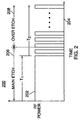
- the method of the present invention as applied to an etch process is illustrated by the timing diagram of FIG. 2.
- RF power 202 is plotted versus time 204.
- the RF power 202 is applied continuously for an initial period of a main etch phase 206 of an integrated circuit process. After the main etch phase has elapsed, the power is pulsed for a transition from the main etch phase to an over etch phase 208 and at least a portion of the over etch phase 208.
- continuous power is applied during a period of time T 1 that encompasses approximately the initial 80% of the main etch phase.
- Pulsed power is applied during a period of time T 2 that encompasses the final 20% of the main etch phase and all of the over etch phase.
- the continuous power, applied during T 1 prevents the formation of undesirable residue, sidewall attack, and process window degradation during the bulk of the etch process.
- the pulsed RF power, applied during T 2 reduces the electron temperature T e and electron density n e of the plasma thereby substantially reducing charging of the wafer 110 and associated damage.
- the duty cycle for the pulsed RF power is typically between about 10% and about 90%.
- the period of the RF pulses is typically between approximately 10 ⁇ s and 1000 ⁇ s.
- the change from continuous power to pulsed power can be triggered by a signal from the process monitor 108 indicating the onset of over etch or other process phase in which the wafer 110 is susceptible to charging damage.
- continuous and pulsed RF power can be applied for empirically predetermined periods of time T 1 and T 2 .
- the process progression is monitored as the wafer is processed using optical emission spectroscopy or another process monitoring technique.
- the routine pulses the RF power supply 105.
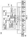
- FIG. 3 shows a block diagram of a processing system 100, such as that depicted in FIG. 1, having such a system controller 140 that can be employed in such a capacity.
- the system controller unit 140 includes a programmable central processing unit (CPU) 302 that is operable with a memory 304, a mass storage device 306, an input control unit 308, and a display unit 310.
- the system controller further includes well-known support circuits 314 such as power supplies 316, clocks 318, cache 320, input/output (I/O) circuits 322 and the like.
- the controller 140 also includes hardware for monitoring wafer processing through sensors (not shown) in the chamber 101. Such sensors measure system parameters such as wafer temperature, chamber atmosphere pressure and the like. All of the above elements are coupled to a control system bus 312.
- the memory 304 contains instructions that the CPU 302 executes to facilitate the performance of the processing system 300.
- the instructions in the memory 304 are in the form of program code such as a program 400 that implements the method of the present invention.
- the program code may conform to any one of a number of different programming languages. For example, the program code can be written in C, C++, BASIC, Pascal, or a number of other languages.
- the mass storage device 306 stores data and instructions and retrieves data and program code instructions from a processor readable storage medium, such as a magnetic disk or magnetic tape.
- a processor readable storage medium such as a magnetic disk or magnetic tape.
- the mass storage device 306 can be a hard disk drive, floppy disk drive, tape drive, or optical disk drive.
- the mass storage device 306 stores and retrieves the instructions in response to directions that it receives from the CPU 302.
- Data and program code instructions that are stored and retrieved by the mass storage device 306 are employed by the processor unit 302 for operating the processing system 100.
- the data and program code instructions are first retrieved by the mass storage device 306 from a medium and then transferred to the memory 304 for use by the CPU 302.
- the input control unit 308 couples a data input device, such as a keyboard, mouse, or light pen, to the processor unit 302 to provide for the receipt of a chamber operator's inputs.
- the display unit 310 provides information to a chamber operator in the form of graphical displays and alphanumeric characters under control of the CPU 302.
- the control system bus 312 provides for the transfer of data and control signals between all of the devices that are coupled to the control system bus 312.
- the control system bus is displayed as a single bus that directly connects the devices in the CPU 302, the control system bus 312 can also be a collection of busses.
- the display unit 310, input control unit 308 and mass storage device 306 can be coupled to an input-output peripheral bus, while the CPU 302 and memory 304 are coupled to a local processor bus.
- the local processor bus and input-output peripheral bus are coupled together to form the control system bus 312.
- the system controller 140 is coupled to the elements of the processing system 100, employed in etch processes in accordance with the present invention via the system bus 312 and the I/O circuits 322. These elements include the following: a plurality of valves 324 (such as valve 124 of FIG. 1), The process monitor 108, the exhaust system 109, the RF power supply 105, the slit valve 114, the gas panel 120, the robot arm 112 and an optional mixer block 326 (not shown in FIG. 1, but may be connected to either the gas panel 120 or chamber 101). The system controller 140 provides signals to the chamber elements that cause these elements to perform operations for etching metal in the chamber 101 of FIG. 1.
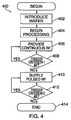
- the CPU 302 forms a general purpose computer that becomes a specific purpose computer when executing programs such as the program 400 of the embodiment of the method of the present invention depicted in the flow diagram of FIG. 4.
- programs such as the program 400 of the embodiment of the method of the present invention depicted in the flow diagram of FIG. 4.
- ASIC application specific integrated circuit
- the program 400 begins, at step 402, with the introduction of a workpiece into the process chamber 101.
- the program 400 executes a first set of instructions that cause the robot arm 112 to insert the wafer 110 through the slit valve 114 and place the wafer 110 on the susceptor 107.
- a second set of instructions retracts the robot arm 112 through the slit valve 114 and closes the slit valve 114.
- step 404 wafer processing begins.
- the program 400 executes a third set of instructions that cause the gas panel 120 to introduce a process gas mixture into the main chamber 101.
- a fourth set of instructions causes the RF power supply 105 to supply RF power to the antenna 102.
- the RF power ignites and sustains the plasma 130 within the chamber 101.
- a gas mixture comprising gases such as Chlorine (Cl 2 ), Boron trichloride (BCl 3 ), and Argon (Ar) is typically provided at a pressure of approximately 9mTorr.
- the gases are provided at a flow rates of about 60 standard cubic centimeters per minute (sccm) for Cl 2 , about 30 sccm for BCl 3 , and about 50 sccm for Ar.
- the RF signal typically has a frequency of approximately 2MHz and a power of about 1300 watts.
- the program 400 monitors conditions within the chamber 101 by, for example, referring to a signal from the process monitor 108.
- the program 400 executes a fourth set of instructions that cause the RF power supply 105 to provide continuous power until a predetermined trigger criterion is reached.
- the program 400 executes a fifth set of instructions that compares the process monitor signal to predetermined signal indicating the onset of the transition from main etch to over etch.
- the program 400 continues to instruct the power supply 105 to provide continuous RF power until the trigger criterion is reached.
- the program 400 can instruct the power supply to provide continuous power for a predetermined period of time T 1 . Such timing can be accomplished by comparing T 1 to a time T measured by the clock 318.
- the program 400 executes, at step 410, a sixth set of instructions that signal RF power supply 105 to supply pulsed RF power to the antenna 102.
- Such instructions can, for example, cause the power supply 105 to turn on and off with a predetermined duty cycle until a second trigger criterion is reached.
- the program 400 executes a seventh set of instructions that compares the process monitor signal to a second predetermined trigger criterion.
- the program 400 continues to instruct the power supply 105 to provide pulsed RF power until the second trigger criterion is reached.
- the program 400 can instruct the power supply 105 to provide pulsed power for a second predetermined period of time T 2 .
- the program ends at step 414.
- the execution of these instructions results in the elements of the processing system 100 being operated to perform a process, such as an etch process, on a semiconductor wafer.
- the system controller 140 may alternatively issue simple "start” and "stop” signals to a dedicated timing circuit built into the RF power supply 105.
- a start signal such a circuit (i.e., a pulse width modulating timer circuit coupled to a power transistor) automatically produces the control signals for driving the power supply 105.
- the control signals cease upon the system controller 140 issuing a stop signal as a result of a trigger criterion or the lapse of a predetermined period of time.
- the advantage of pulsed RF power during the transition to over etch is readily apparent from the graph depicted in FIG. 5.
- the graph 500 shows electron temperature T e 502 and density n e 504 as functions of time in microseconds ( ⁇ s) during a RF pulse.
- the RF power was applied during an over etch portion of an etch process according to the method of the present invention.
- the RF power was pulsed with a period of 200 ⁇ s and a 50% duty cycle.
- RF power was applied during an "on" portion 506 of the pulse lasting approximately 100 ⁇ s.
- the RF power of approximately 1300 watts was turned off during an "off" portion 508 lasting approximately 100 ⁇ s.
- Cl 2 , BCl 3 and Ar were provided at flow rates of 60, 30 and 50 sccm respectively.
- the electron temperature T e 502 remains approximately constant and electron density n e slowly increases.
- both T e and n e drop abruptly to near zero within 20 and 40 ⁇ s respectively.
- the rapid drop in T e decreases the energy with which electrons impinge upon the wafer 110.
- the rapid drop in n e decreases the rate at which electrons impinge upon the wafer 110. Both effects decrease charging of the wafer 110 and avoid charging damage.
- the foregoing embodiment used continuous power followed by pulsed power in an etch reactor to reduce topographical charging.
- the invention also finds use in plasma enhanced deposition processes, such as dielectric deposition, where topographical charging may occur at the beginning of the deposition process. Consequently, pulsed power is used at the beginning of the deposition process followed by continuous power during bulk deposition.
- the foregoing embodiment described two phases of plasma processing.
- the invention may be used in a multiphase process, where the plasma is created using continuous power, then pulsed power, then continuous power, then pulsed power and so on, or the plasma is created using pulsed power, then continuous power, then pulsed power, then continuous power and so on.
- Wafers containing high aspect ratio structures are prone to topography dependent charging. As such, the invention is greatly beneficial in processing of wafers with high aspect ratio structures.
Landscapes
- Physics & Mathematics (AREA)
- Engineering & Computer Science (AREA)
- Plasma & Fusion (AREA)
- Chemical & Material Sciences (AREA)
- Analytical Chemistry (AREA)
- Drying Of Semiconductors (AREA)
Abstract
Description
Claims (35)
- A method for processing a semiconductor wafer, comprising the steps of:forming a plasma proximate the wafer;applying continuous RF power to said plasma while processing the wafer with said plasma for a first phase of a process; andprocessing said wafer with pulsed RF power for a second phase of said process.
- The method of claim 1, wherein said process is an etch process.
- The method of any one of the proceeding claims, wherein said first phase is performed before said second phase.
- The method of any one of claims 1 or 2, wherein said second phase is performed before said first phase.
- The method of any one of the proceeding claims, further comprising performing herein multiple phases of a process, where each phase includes applying either continuous or pulsed RF power to from said plasma.
- The method of any one of the proceedings claims, wherein said first phase includes an initial portion of a main etch process.
- The method of claim 6, wherein said second phase includes a final portion of a main etch process and at least a portion of an over etch process.
- The method of claim 6, wherein said first phase is approximately the initial 80% of said main etch process.
- The method of any one of the proceedings claims, wherein a duty cycle for said pulsed RF power is between approximately 10 percent and 90 percent.
- The method of any one of the proceeding claims, wherein a period for said pulsed RF power is between about 10 µs and about 1000 µs.
- The method of any one of the proceeding claims, wherein said second phase is a beginning of a plasma enhanced deposition process and said first phase is a bulk deposition process.
- The method of any one of the proceeding claims, further comprising the step of monitoring a condition of said process.
- The method of claim 12, wherein said pulsed power is initiated in a response to a change in said condition.
- The method of any of claims 12 to 13, wherein said condition is an optical emission.
- The method of any one of the proceeding claims, wherein the wafer comprises high aspect ratio structures.
- The method of any one of the proceeding claims, wherein said plasma is a high density plasma.
- A method for etching a semiconductor wafer with a system having a chamber and a RF power source, comprising the steps of:providing RF power from the RF power source to form a plasma in the chamberapplying continuous RF power to said plasma while etching the wafer with said plasma during a first phase of a main etch process; andapplying pulsed RF power for a subsequent phase of said etch process.
- The method of claim 17, wherein said subsequent phase includes a final portion of the main etch process and at least a portion of an over etch process.
- The method of any one of claims 17 to 18, wherein said first phase is approximately the initial 80% of said main etch step.
- The method of any one of claim 17 to 19, further comprising the step of monitoring a condition of said process and applying said pulsed power in response to a change in said condition.
- The method of claim 20, wherein said condition is an optical emission.
- A computer readable storage medium having program code embodied therein, said program code for controlling a semiconductor processing system during a wafer fabrication process, wherein said semiconductor processing system includes a chamber and a RF power supply, said program code controlling the semiconductor processing system in accordance with the following steps:applying continuous RF power for a first phase of a process; andapplying pulsed RF power to said plasma for a second phase of said process.
- The computer readable storage medium of claim 22, wherein said first phase includes an initial portion of a duration of a main etch process.
- The computer readable storage medium of claim 23, wherein said second phase includes a final portion of said main etch process and at least a portion of an over etch process.
- The computer readable storage medium of any one of claims 23 to 24, wherein said initial portion is approximately the initial 80% of said main etch process.
- The computer readable storage medium of any one of claims 22 to 25, wherein said program code further comprises the step of monitoring a condition of said process and applying said pulsed power in response to a change in said condition.
- The computer readable storage medium of any one of claims 22 to 26, wherein said first phase occurs before said second phase.
- The computer readable storage medium of any one of claims 22 to 26, wherein said second phase occurs before said first phase.
- Apparatus for processing a wafer (110) comprising:a vacuum chamber comprising a wafer support (107);a plasma generator (105) coupled to said vacuum chamber;a controller (140) coupled to said plasma generator, for controlling the plasma generator, where said plasma generator produces continuous RF power while processing a wafer during a first phase of a process, and produces pulsed RF power during a second phase of said process.
- The apparatus of claim 28, wherein said plasma generator comprises:a coil (102);an RF power supply (105).
- The apparatus of claim 30, wherein the coil is an antenna.
- The apparatus of any one of claims 29 to 31, wherein said process is a plasma process.
- The apparatus of claim 32, wherein said plasma process is a high density plasma process.
- The apparatus of any one of claims 29 to 33, further comprising:a process monitor coupled to said controller.
- The apparatus of claim 34, wherein said process monitor produces a signal that causes said controller to switch from the first phase to the second phase.
Applications Claiming Priority (2)
| Application Number | Priority Date | Filing Date | Title |
|---|---|---|---|
| US09/360,883 US6566272B2 (en) | 1999-07-23 | 1999-07-23 | Method for providing pulsed plasma during a portion of a semiconductor wafer process |
| US360883 | 1999-07-23 |
Publications (2)
| Publication Number | Publication Date |
|---|---|
| EP1071120A2 true EP1071120A2 (en) | 2001-01-24 |
| EP1071120A3 EP1071120A3 (en) | 2001-04-11 |
Family
ID=23419784
Family Applications (1)
| Application Number | Title | Priority Date | Filing Date |
|---|---|---|---|
| EP00115860A Withdrawn EP1071120A3 (en) | 1999-07-23 | 2000-07-24 | Method for providing pulsed plasma during a portion of a semiconductor wafer process |
Country Status (4)
| Country | Link |
|---|---|
| US (1) | US6566272B2 (en) |
| EP (1) | EP1071120A3 (en) |
| JP (1) | JP5197898B2 (en) |
| KR (1) | KR100756737B1 (en) |
Cited By (5)
| Publication number | Priority date | Publication date | Assignee | Title |
|---|---|---|---|---|
| GB2368193A (en) * | 2000-06-29 | 2002-04-24 | Nec Corp | Semiconductor etching method |
| WO2003107382A3 (en) * | 2002-06-12 | 2004-09-23 | Applied Materials Inc | PLASMA PROCESS AND DEVICE FOR PROCESSING A SUBSTRATE |
| KR100461779B1 (en) * | 2001-06-11 | 2004-12-14 | 엔이씨 일렉트로닉스 가부시키가이샤 | Method of manufacturing semiconductor devices and semiconductor manufacturing apparatus |
| US6942813B2 (en) | 2003-03-05 | 2005-09-13 | Applied Materials, Inc. | Method of etching magnetic and ferroelectric materials using a pulsed bias source |
| CN110246743A (en) * | 2014-10-20 | 2019-09-17 | 朗姆研究公司 | The system and method for detection processing point in multi-mode pulse processing |
Families Citing this family (42)
| Publication number | Priority date | Publication date | Assignee | Title |
|---|---|---|---|---|
| US20030003748A1 (en) * | 2001-05-24 | 2003-01-02 | Anisul Khan | Method of eliminating notching when anisotropically etching small linewidth openings in silicon on insulator |
| KR100457742B1 (en) * | 2002-05-16 | 2004-11-18 | 주식회사 하이닉스반도체 | Method for forming a gate of semiconductor device |
| US6673200B1 (en) * | 2002-05-30 | 2004-01-06 | Lsi Logic Corporation | Method of reducing process plasma damage using optical spectroscopy |
| US7357748B2 (en) * | 2004-07-13 | 2008-04-15 | Borgwarner Inc. | Limited slip differential |
| US7141514B2 (en) * | 2005-02-02 | 2006-11-28 | Applied Materials, Inc. | Selective plasma re-oxidation process using pulsed RF source power |
| US7214628B2 (en) * | 2005-02-02 | 2007-05-08 | Applied Materials, Inc. | Plasma gate oxidation process using pulsed RF source power |
| US7985688B2 (en) * | 2005-12-16 | 2011-07-26 | Lam Research Corporation | Notch stop pulsing process for plasma processing system |
| US20080011426A1 (en) * | 2006-01-30 | 2008-01-17 | Applied Materials, Inc. | Plasma reactor with inductively coupled source power applicator and a high temperature heated workpiece support |
| US7718538B2 (en) * | 2007-02-21 | 2010-05-18 | Applied Materials, Inc. | Pulsed-plasma system with pulsed sample bias for etching semiconductor substrates |
| WO2008103453A1 (en) * | 2007-02-21 | 2008-08-28 | Applied Materials, Inc. | Pulsed plasma system with pulsed reaction gas replenish for etching semiconductor structures |
| US7771606B2 (en) * | 2007-02-22 | 2010-08-10 | Applied Materials, Inc. | Pulsed-plasma system with pulsed reaction gas replenish for etching semiconductors structures |
| US7737042B2 (en) * | 2007-02-22 | 2010-06-15 | Applied Materials, Inc. | Pulsed-plasma system for etching semiconductor structures |
| WO2008103454A2 (en) * | 2007-02-21 | 2008-08-28 | Applied Materials, Inc. | Pulsed plasma system for etching semiconductor structures |
| US20080230008A1 (en) * | 2007-03-21 | 2008-09-25 | Alexander Paterson | Plasma species and uniformity control through pulsed vhf operation |
| US20090004873A1 (en) * | 2007-06-26 | 2009-01-01 | Intevac, Inc. | Hybrid etch chamber with decoupled plasma controls |
| JP5221403B2 (en) | 2009-01-26 | 2013-06-26 | 東京エレクトロン株式会社 | Plasma etching method, plasma etching apparatus and storage medium |
| US8659335B2 (en) | 2009-06-25 | 2014-02-25 | Mks Instruments, Inc. | Method and system for controlling radio frequency power |
| JP5461148B2 (en) * | 2009-11-05 | 2014-04-02 | 株式会社日立ハイテクノロジーズ | Plasma etching method and apparatus |
| WO2011068927A2 (en) * | 2009-12-04 | 2011-06-09 | Abbott Laboratories | 11-β-HYDROXYSTEROID DEHYDROGENASE TYPE 1 (11B-HSD1) INHIBITORS AND USES THEREOF |
| US8658541B2 (en) * | 2010-01-15 | 2014-02-25 | Applied Materials, Inc. | Method of controlling trench microloading using plasma pulsing |
| US20130048082A1 (en) * | 2011-08-22 | 2013-02-28 | Mirzafer Abatchev | System, method and apparatus for real time control of rapid alternating processes (rap) |
| US9685297B2 (en) | 2012-08-28 | 2017-06-20 | Advanced Energy Industries, Inc. | Systems and methods for monitoring faults, anomalies, and other characteristics of a switched mode ion energy distribution system |
| JP6114622B2 (en) * | 2013-04-26 | 2017-04-12 | 東京エレクトロン株式会社 | Etching method |
| JP6043852B2 (en) * | 2015-10-01 | 2016-12-14 | 株式会社日立ハイテクノロジーズ | Plasma processing equipment |
| US9978606B2 (en) | 2015-10-02 | 2018-05-22 | Applied Materials, Inc. | Methods for atomic level resolution and plasma processing control |
| US9788405B2 (en) | 2015-10-03 | 2017-10-10 | Applied Materials, Inc. | RF power delivery with approximated saw tooth wave pulsing |
| US9741539B2 (en) | 2015-10-05 | 2017-08-22 | Applied Materials, Inc. | RF power delivery regulation for processing substrates |
| US9754767B2 (en) | 2015-10-13 | 2017-09-05 | Applied Materials, Inc. | RF pulse reflection reduction for processing substrates |
| US9614524B1 (en) | 2015-11-28 | 2017-04-04 | Applied Materials, Inc. | Automatic impedance tuning with RF dual level pulsing |
| GB201705202D0 (en) * | 2017-03-31 | 2017-05-17 | Univ Dublin City | System and method for remote sensing a plasma |
| JP7235761B2 (en) * | 2017-11-17 | 2023-03-08 | エーイーエス グローバル ホールディングス, プライベート リミテッド | Synchronous pulsing of plasma processing source and substrate bias |
| TWI872423B (en) | 2017-11-17 | 2025-02-11 | 新加坡商Aes 全球公司 | Systems and methods for spatially and temporally controlling plasma processing on substrates and related computer-readable medium |
| US12230476B2 (en) | 2017-11-17 | 2025-02-18 | Advanced Energy Industries, Inc. | Integrated control of a plasma processing system |
| US11437221B2 (en) | 2017-11-17 | 2022-09-06 | Advanced Energy Industries, Inc. | Spatial monitoring and control of plasma processing environments |
| US12505986B2 (en) | 2017-11-17 | 2025-12-23 | Advanced Energy Industries, Inc. | Synchronization of plasma processing components |
| US20210343506A1 (en) * | 2020-05-01 | 2021-11-04 | Mattson Technology, Inc. | Methods And Apparatus For Pulsed Inductively Coupled Plasma For Surface Treatment Processing |
| KR102587031B1 (en) * | 2021-06-01 | 2023-10-12 | 충남대학교산학협력단 | Adaptive pulsed process apparatus and method for high aspect ratio contact and recording medium storing program for executing the same, and computer program stored in recording medium for executing the same |
| US12046448B2 (en) | 2022-01-26 | 2024-07-23 | Advanced Energy Industries, Inc. | Active switch on time control for bias supply |
| US11942309B2 (en) | 2022-01-26 | 2024-03-26 | Advanced Energy Industries, Inc. | Bias supply with resonant switching |
| US11670487B1 (en) | 2022-01-26 | 2023-06-06 | Advanced Energy Industries, Inc. | Bias supply control and data processing |
| US11978613B2 (en) | 2022-09-01 | 2024-05-07 | Advanced Energy Industries, Inc. | Transition control in a bias supply |
| US12567572B2 (en) | 2023-07-11 | 2026-03-03 | Advanced Energy Industries, Inc. | Plasma behaviors predicted by current measurements during asymmetric bias waveform application |
Family Cites Families (63)
| Publication number | Priority date | Publication date | Assignee | Title |
|---|---|---|---|---|
| US4163172A (en) | 1977-07-08 | 1979-07-31 | Systems, Science And Software | Sliding spark source cold cathode electron gun and method |
| US4357195A (en) * | 1979-06-25 | 1982-11-02 | Tegal Corporation | Apparatus for controlling a plasma reaction |
| US4263088A (en) * | 1979-06-25 | 1981-04-21 | Motorola, Inc. | Method for process control of a plasma reaction |
| JPS5930130B2 (en) | 1979-09-20 | 1984-07-25 | 富士通株式会社 | Vapor phase growth method |
| US4570106A (en) | 1982-02-18 | 1986-02-11 | Elscint, Inc. | Plasma electron source for cold-cathode discharge device or the like |
| JPS611023A (en) | 1984-06-13 | 1986-01-07 | Teru Saamuko Kk | Batch plasma device |
| DE3733135C1 (en) | 1987-10-01 | 1988-09-22 | Leybold Ag | Device for coating or etching using a plasma |
| GB2212974B (en) | 1987-11-25 | 1992-02-12 | Fuji Electric Co Ltd | Plasma processing apparatus |
| JPH06104898B2 (en) | 1988-01-13 | 1994-12-21 | 忠弘 大見 | Decompression surface treatment equipment |
| US4963239A (en) | 1988-01-29 | 1990-10-16 | Hitachi, Ltd. | Sputtering process and an apparatus for carrying out the same |
| US4837185A (en) | 1988-10-26 | 1989-06-06 | Intel Corporation | Pulsed dual radio frequency CVD process |
| DE3841730C2 (en) | 1988-12-10 | 1997-06-19 | Widia Gmbh | Process for coating a metallic base body with a non-conductive coating material |
| DE3841731C1 (en) | 1988-12-10 | 1990-04-12 | Krupp Widia Gmbh, 4300 Essen, De | Process for coating a tool base, and tool produced by this process |
| EP0395415B1 (en) | 1989-04-27 | 1995-03-15 | Fujitsu Limited | Apparatus for and method of processing a semiconductor device using microwave-generated plasma |
| US4889588A (en) | 1989-05-01 | 1989-12-26 | Tegal Corporation | Plasma etch isotropy control |
| JPH02309631A (en) * | 1989-05-24 | 1990-12-25 | Matsushita Electron Corp | Plasma etching method |
| JP2972227B2 (en) | 1989-05-29 | 1999-11-08 | 株式会社日立製作所 | Plasma processing method and apparatus |
| US5013578A (en) | 1989-12-11 | 1991-05-07 | University Of California | Apparatus for coating a surface with a metal utilizing a plasma source |
| US5160408A (en) | 1990-04-27 | 1992-11-03 | Micron Technology, Inc. | Method of isotropically dry etching a polysilicon containing runner with pulsed power |
| KR930004713B1 (en) | 1990-06-18 | 1993-06-03 | 삼성전자 주식회사 | Plasma Generator and Method Using Modulation |
| US5707486A (en) | 1990-07-31 | 1998-01-13 | Applied Materials, Inc. | Plasma reactor using UHF/VHF and RF triode source, and process |
| US5259922A (en) * | 1990-08-14 | 1993-11-09 | Matsushita Electric Industrial Co., Ltd. | Drying etching method |
| JP2687966B2 (en) | 1990-08-20 | 1997-12-08 | 富士通株式会社 | Method for manufacturing semiconductor device |
| US5273609A (en) | 1990-09-12 | 1993-12-28 | Texas Instruments Incorporated | Method and apparatus for time-division plasma chopping in a multi-channel plasma processing equipment |
| US5057185A (en) | 1990-09-27 | 1991-10-15 | Consortium For Surface Processing, Inc. | Triode plasma reactor with phase modulated plasma control |
| JPH04144992A (en) | 1990-10-01 | 1992-05-19 | Idemitsu Petrochem Co Ltd | Microwave plasma-generating device and method for producing diamond film with the same |
| DE4122452C2 (en) | 1991-07-06 | 1993-10-28 | Schott Glaswerke | Method and device for igniting CVD plasmas |
| JPH0521392A (en) | 1991-07-17 | 1993-01-29 | Fuji Electric Co Ltd | Plasma processing device |
| US5212118A (en) | 1991-08-09 | 1993-05-18 | Saxena Arjun N | Method for selective chemical vapor deposition of dielectric, semiconductor and conductive films on semiconductor and metallic substrates |
| JPH05299378A (en) | 1992-04-21 | 1993-11-12 | I N R Kenkyusho:Kk | Plasma processing device |
| JP2988122B2 (en) | 1992-05-14 | 1999-12-06 | 日本電気株式会社 | Dry etching apparatus and method for manufacturing semiconductor device |
| JP2584389B2 (en) | 1992-06-10 | 1997-02-26 | 栄電子工業 株式会社 | ECR plasma etching method |
| JP2590393B2 (en) | 1992-06-10 | 1997-03-12 | 栄電子工業 株式会社 | ECR plasma etching method |
| JP2941572B2 (en) | 1992-08-11 | 1999-08-25 | 三菱電機株式会社 | Plasma etching apparatus and method for manufacturing semiconductor device |
| JPH06342769A (en) | 1992-08-21 | 1994-12-13 | Nissin Electric Co Ltd | Etching method and apparatus |
| JP2584396B2 (en) | 1992-10-08 | 1997-02-26 | 栄電子工業 株式会社 | ECR plasma processing method |
| JP2693899B2 (en) | 1992-10-09 | 1997-12-24 | 栄電子工業株式会社 | ECR plasma processing method |
| US5346578A (en) | 1992-11-04 | 1994-09-13 | Novellus Systems, Inc. | Induction plasma source |
| US5352324A (en) | 1992-11-05 | 1994-10-04 | Hitachi, Ltd. | Etching method and etching apparatus therefor |
| JPH06181185A (en) | 1992-12-14 | 1994-06-28 | Toshiba Corp | Plasma surface treating system |
| JPH06216047A (en) | 1993-01-12 | 1994-08-05 | Anelva Corp | Method and apparatus for forming microwave plasma CVD film |
| JP3430552B2 (en) | 1993-05-07 | 2003-07-28 | ソニー株式会社 | Manufacturing method of diamond semiconductor |
| KR100302167B1 (en) | 1993-11-05 | 2001-11-22 | 히가시 데쓰로 | Plasma Treatment Equipment and Plasma Treatment Methods |
| US5532495A (en) | 1993-11-16 | 1996-07-02 | Sandia Corporation | Methods and apparatus for altering material using ion beams |
| US5468296A (en) | 1993-12-17 | 1995-11-21 | Lsi Logic Corporation | Apparatus for igniting low pressure inductively coupled plasma |
| US5468341A (en) | 1993-12-28 | 1995-11-21 | Nec Corporation | Plasma-etching method and apparatus therefor |
| JP3365067B2 (en) | 1994-02-10 | 2003-01-08 | ソニー株式会社 | Plasma apparatus and plasma processing method using the same |
| US5460689A (en) * | 1994-02-28 | 1995-10-24 | Applied Materials, Inc. | High pressure plasma treatment method and apparatus |
| JPH07273071A (en) * | 1994-04-01 | 1995-10-20 | Sony Corp | Plasma etching method |
| US5558718A (en) | 1994-04-08 | 1996-09-24 | The Regents, University Of California | Pulsed source ion implantation apparatus and method |
| US5651865A (en) | 1994-06-17 | 1997-07-29 | Eni | Preferential sputtering of insulators from conductive targets |
| JPH0892765A (en) | 1994-09-22 | 1996-04-09 | Tokyo Electron Ltd | Etching method |
| JP3546977B2 (en) * | 1994-10-14 | 2004-07-28 | 富士通株式会社 | Semiconductor device manufacturing method and manufacturing apparatus |
| JP2845163B2 (en) | 1994-10-27 | 1999-01-13 | 日本電気株式会社 | Plasma processing method and apparatus |
| US5597495A (en) * | 1994-11-07 | 1997-01-28 | Keil; Mark | Method and apparatus for etching surfaces with atomic fluorine |
| US5683538A (en) | 1994-12-23 | 1997-11-04 | International Business Machines Corporation | Control of etch selectivity |
| US5614060A (en) | 1995-03-23 | 1997-03-25 | Applied Materials, Inc. | Process and apparatus for etching metal in integrated circuit structure with high selectivity to photoresist and good metal etch residue removal |
| US5696428A (en) | 1995-06-07 | 1997-12-09 | Lsi Logic Corporation | Apparatus and method using optical energy for specifying and quantitatively controlling chemically-reactive components of semiconductor processing plasma etching gas |
| JP2783276B2 (en) | 1995-07-04 | 1998-08-06 | 日本電気株式会社 | Method for manufacturing semiconductor device |
| US5534751A (en) | 1995-07-10 | 1996-07-09 | Lam Research Corporation | Plasma etching apparatus utilizing plasma confinement |
| US5800688A (en) | 1997-04-21 | 1998-09-01 | Tokyo Electron Limited | Apparatus for ionized sputtering |
| US5910011A (en) | 1997-05-12 | 1999-06-08 | Applied Materials, Inc. | Method and apparatus for monitoring processes using multiple parameters of a semiconductor wafer processing system |
| JPH10312899A (en) * | 1997-05-15 | 1998-11-24 | Matsushita Electric Ind Co Ltd | Plasma processing method and plasma processing apparatus |
-
1999
- 1999-07-23 US US09/360,883 patent/US6566272B2/en not_active Expired - Lifetime
-
2000
- 2000-07-24 EP EP00115860A patent/EP1071120A3/en not_active Withdrawn
- 2000-07-24 KR KR1020000042402A patent/KR100756737B1/en not_active Expired - Fee Related
- 2000-07-24 JP JP2000256459A patent/JP5197898B2/en not_active Expired - Fee Related
Cited By (6)
| Publication number | Priority date | Publication date | Assignee | Title |
|---|---|---|---|---|
| GB2368193A (en) * | 2000-06-29 | 2002-04-24 | Nec Corp | Semiconductor etching method |
| KR100461779B1 (en) * | 2001-06-11 | 2004-12-14 | 엔이씨 일렉트로닉스 가부시키가이샤 | Method of manufacturing semiconductor devices and semiconductor manufacturing apparatus |
| WO2003107382A3 (en) * | 2002-06-12 | 2004-09-23 | Applied Materials Inc | PLASMA PROCESS AND DEVICE FOR PROCESSING A SUBSTRATE |
| CN100533651C (en) * | 2002-06-12 | 2009-08-26 | 应用材料有限公司 | Plasma apparatus and method for processing a substrate |
| US6942813B2 (en) | 2003-03-05 | 2005-09-13 | Applied Materials, Inc. | Method of etching magnetic and ferroelectric materials using a pulsed bias source |
| CN110246743A (en) * | 2014-10-20 | 2019-09-17 | 朗姆研究公司 | The system and method for detection processing point in multi-mode pulse processing |
Also Published As
| Publication number | Publication date |
|---|---|
| US6566272B2 (en) | 2003-05-20 |
| JP2002050611A (en) | 2002-02-15 |
| KR100756737B1 (en) | 2007-09-07 |
| EP1071120A3 (en) | 2001-04-11 |
| US20020052111A1 (en) | 2002-05-02 |
| KR20010039749A (en) | 2001-05-15 |
| JP5197898B2 (en) | 2013-05-15 |
Similar Documents
| Publication | Publication Date | Title |
|---|---|---|
| US6566272B2 (en) | Method for providing pulsed plasma during a portion of a semiconductor wafer process | |
| US6599842B2 (en) | Method for rounding corners and removing damaged outer surfaces of a trench | |
| US7138067B2 (en) | Methods and apparatus for tuning a set of plasma processing steps | |
| US9530666B2 (en) | Plasma etching method and plasma etching apparatus | |
| JP2918892B2 (en) | Plasma etching method | |
| US5476182A (en) | Etching apparatus and method therefor | |
| US5618382A (en) | High-frequency semiconductor wafer processing apparatus and method | |
| US9349603B2 (en) | Plasma processing method | |
| US20030132198A1 (en) | Method and apparatus for treating surface of semiconductor | |
| US20140349493A1 (en) | Methods and apparatuses for energetic neutral flux generation for processing a substrate | |
| JP2003234340A (en) | High frequency plasma processing method and high frequency plasma processing apparatus | |
| JP2004507086A (en) | Substrate processing method and processing system | |
| KR102797229B1 (en) | Plasma processing method and plasma processing apparatus | |
| JP2634313B2 (en) | Plasma processing method for semiconductor wafer production | |
| US6303513B1 (en) | Method for controlling a profile of a structure formed on a substrate | |
| JP2001168086A (en) | Semiconductor device manufacturing method and manufacturing apparatus | |
| JP2845199B2 (en) | Dry etching apparatus and dry etching method | |
| WO2008049024A1 (en) | Methods and apparatus for tuning a set of plasma processing steps | |
| KR20160003624A (en) | Etching method | |
| JPH07201814A (en) | Plasma etching method | |
| JPH1064886A (en) | Dry etching apparatus and dry etching method | |
| US20070000869A1 (en) | Etching method in a semiconductor processing and etching system for performing the same | |
| JP3002033B2 (en) | Dry etching method | |
| JPWO1997011207A1 (en) | Dry Etching Method | |
| JP3732079B2 (en) | Sample surface processing method |
Legal Events
| Date | Code | Title | Description |
|---|---|---|---|
| PUAI | Public reference made under article 153(3) epc to a published international application that has entered the european phase |
Free format text: ORIGINAL CODE: 0009012 |
|
| AK | Designated contracting states |
Kind code of ref document: A2 Designated state(s): GB |
|
| AX | Request for extension of the european patent |
Free format text: AL;LT;LV;MK;RO;SI |
|
| PUAL | Search report despatched |
Free format text: ORIGINAL CODE: 0009013 |
|
| AK | Designated contracting states |
Kind code of ref document: A3 Designated state(s): AT BE CH CY DE DK ES FI FR GB GR IE IT LI LU MC NL PT SE |
|
| AX | Request for extension of the european patent |
Free format text: AL;LT;LV;MK;RO;SI |
|
| RIC1 | Information provided on ipc code assigned before grant |
Free format text: 7H 01L 21/3065 A, 7H 01J 37/32 B, 7H 01L 21/3213 B |
|
| RIN1 | Information on inventor provided before grant (corrected) |
Inventor name: YAMARTINO, JOHN M. Inventor name: LOEWENHARDT, PETER K. Inventor name: PATERSON, ALEX Inventor name: ZAWALSKI, WADE |
|
| 17P | Request for examination filed |
Effective date: 20010618 |
|
| AKX | Designation fees paid |
Free format text: GB |
|
| REG | Reference to a national code |
Ref country code: DE Ref legal event code: 8566 |
|
| STAA | Information on the status of an ep patent application or granted ep patent |
Free format text: STATUS: THE APPLICATION HAS BEEN WITHDRAWN |
|
| 18W | Application withdrawn |
Effective date: 20050128 |