EP1070768B1 - Verfahren zur Herstellung von Monolagen aus Silizium-Nanoclustern in Siliziumdioxid - Google Patents
Verfahren zur Herstellung von Monolagen aus Silizium-Nanoclustern in Siliziumdioxid Download PDFInfo
- Publication number
- EP1070768B1 EP1070768B1 EP00114817A EP00114817A EP1070768B1 EP 1070768 B1 EP1070768 B1 EP 1070768B1 EP 00114817 A EP00114817 A EP 00114817A EP 00114817 A EP00114817 A EP 00114817A EP 1070768 B1 EP1070768 B1 EP 1070768B1
- Authority
- EP
- European Patent Office
- Prior art keywords
- silicon
- layer
- sio
- ion
- silicon oxide
- Prior art date
- Legal status (The legal status is an assumption and is not a legal conclusion. Google has not performed a legal analysis and makes no representation as to the accuracy of the status listed.)
- Expired - Lifetime
Links
Images

Classifications
-
- H—ELECTRICITY
- H10—SEMICONDUCTOR DEVICES; ELECTRIC SOLID-STATE DEVICES NOT OTHERWISE PROVIDED FOR
- H10P—GENERIC PROCESSES OR APPARATUS FOR THE MANUFACTURE OR TREATMENT OF DEVICES COVERED BY CLASS H10
- H10P30/00—Ion implantation into wafers, substrates or parts of devices
- H10P30/20—Ion implantation into wafers, substrates or parts of devices into semiconductor materials, e.g. for doping
- H10P30/202—Ion implantation into wafers, substrates or parts of devices into semiconductor materials, e.g. for doping characterised by the semiconductor materials
- H10P30/204—Ion implantation into wafers, substrates or parts of devices into semiconductor materials, e.g. for doping characterised by the semiconductor materials into Group IV semiconductors
-
- C—CHEMISTRY; METALLURGY
- C23—COATING METALLIC MATERIAL; COATING MATERIAL WITH METALLIC MATERIAL; CHEMICAL SURFACE TREATMENT; DIFFUSION TREATMENT OF METALLIC MATERIAL; COATING BY VACUUM EVAPORATION, BY SPUTTERING, BY ION IMPLANTATION OR BY CHEMICAL VAPOUR DEPOSITION, IN GENERAL; INHIBITING CORROSION OF METALLIC MATERIAL OR INCRUSTATION IN GENERAL
- C23C—COATING METALLIC MATERIAL; COATING MATERIAL WITH METALLIC MATERIAL; SURFACE TREATMENT OF METALLIC MATERIAL BY DIFFUSION INTO THE SURFACE, BY CHEMICAL CONVERSION OR SUBSTITUTION; COATING BY VACUUM EVAPORATION, BY SPUTTERING, BY ION IMPLANTATION OR BY CHEMICAL VAPOUR DEPOSITION, IN GENERAL
- C23C14/00—Coating by vacuum evaporation, by sputtering or by ion implantation of the coating forming material
- C23C14/22—Coating by vacuum evaporation, by sputtering or by ion implantation of the coating forming material characterised by the process of coating
- C23C14/48—Ion implantation
-
- H—ELECTRICITY
- H10—SEMICONDUCTOR DEVICES; ELECTRIC SOLID-STATE DEVICES NOT OTHERWISE PROVIDED FOR
- H10D—INORGANIC ELECTRIC SEMICONDUCTOR DEVICES
- H10D30/00—Field-effect transistors [FET]
- H10D30/01—Manufacture or treatment
- H10D30/021—Manufacture or treatment of FETs having insulated gates [IGFET]
- H10D30/0223—Manufacture or treatment of FETs having insulated gates [IGFET] having source and drain regions or source and drain extensions self-aligned to sides of the gate
-
- H—ELECTRICITY
- H10—SEMICONDUCTOR DEVICES; ELECTRIC SOLID-STATE DEVICES NOT OTHERWISE PROVIDED FOR
- H10D—INORGANIC ELECTRIC SEMICONDUCTOR DEVICES
- H10D64/00—Electrodes of devices having potential barriers
- H10D64/01—Manufacture or treatment
- H10D64/013—Manufacture or treatment of electrodes having a conductor capacitively coupled to a semiconductor by an insulator
- H10D64/01302—Manufacture or treatment of electrodes having a conductor capacitively coupled to a semiconductor by an insulator the insulator being formed after the semiconductor body, the semiconductor being silicon
- H10D64/01332—Making the insulator
- H10D64/01336—Making the insulator on single crystalline silicon, e.g. chemical oxidation using a liquid
- H10D64/01338—Making the insulator on single crystalline silicon, e.g. chemical oxidation using a liquid with a treatment, e.g. annealing, after the formation of the conductor
-
- H—ELECTRICITY
- H10—SEMICONDUCTOR DEVICES; ELECTRIC SOLID-STATE DEVICES NOT OTHERWISE PROVIDED FOR
- H10D—INORGANIC ELECTRIC SEMICONDUCTOR DEVICES
- H10D64/00—Electrodes of devices having potential barriers
- H10D64/01—Manufacture or treatment
- H10D64/013—Manufacture or treatment of electrodes having a conductor capacitively coupled to a semiconductor by an insulator
- H10D64/01302—Manufacture or treatment of electrodes having a conductor capacitively coupled to a semiconductor by an insulator the insulator being formed after the semiconductor body, the semiconductor being silicon
- H10D64/01332—Making the insulator
- H10D64/01336—Making the insulator on single crystalline silicon, e.g. chemical oxidation using a liquid
- H10D64/0134—Making the insulator on single crystalline silicon, e.g. chemical oxidation using a liquid with a treatment, e.g. annealing, after the formation of the insulator and before the formation of the conductor
-
- H—ELECTRICITY
- H10—SEMICONDUCTOR DEVICES; ELECTRIC SOLID-STATE DEVICES NOT OTHERWISE PROVIDED FOR
- H10D—INORGANIC ELECTRIC SEMICONDUCTOR DEVICES
- H10D64/00—Electrodes of devices having potential barriers
- H10D64/01—Manufacture or treatment
- H10D64/031—Manufacture or treatment of data-storage electrodes
- H10D64/037—Manufacture or treatment of data-storage electrodes comprising charge-trapping insulators
-
- H—ELECTRICITY
- H10—SEMICONDUCTOR DEVICES; ELECTRIC SOLID-STATE DEVICES NOT OTHERWISE PROVIDED FOR
- H10D—INORGANIC ELECTRIC SEMICONDUCTOR DEVICES
- H10D64/00—Electrodes of devices having potential barriers
- H10D64/60—Electrodes characterised by their materials
- H10D64/66—Electrodes having a conductor capacitively coupled to a semiconductor by an insulator, e.g. MIS electrodes
- H10D64/68—Electrodes having a conductor capacitively coupled to a semiconductor by an insulator, e.g. MIS electrodes characterised by the insulator, e.g. by the gate insulator
- H10D64/693—Electrodes having a conductor capacitively coupled to a semiconductor by an insulator, e.g. MIS electrodes characterised by the insulator, e.g. by the gate insulator the insulator comprising nitrogen, e.g. nitrides, oxynitrides or nitrogen-doped materials
-
- H—ELECTRICITY
- H10—SEMICONDUCTOR DEVICES; ELECTRIC SOLID-STATE DEVICES NOT OTHERWISE PROVIDED FOR
- H10P—GENERIC PROCESSES OR APPARATUS FOR THE MANUFACTURE OR TREATMENT OF DEVICES COVERED BY CLASS H10
- H10P30/00—Ion implantation into wafers, substrates or parts of devices
- H10P30/20—Ion implantation into wafers, substrates or parts of devices into semiconductor materials, e.g. for doping
- H10P30/208—Ion implantation into wafers, substrates or parts of devices into semiconductor materials, e.g. for doping of electrically inactive species
-
- H—ELECTRICITY
- H10—SEMICONDUCTOR DEVICES; ELECTRIC SOLID-STATE DEVICES NOT OTHERWISE PROVIDED FOR
- H10P—GENERIC PROCESSES OR APPARATUS FOR THE MANUFACTURE OR TREATMENT OF DEVICES COVERED BY CLASS H10
- H10P30/00—Ion implantation into wafers, substrates or parts of devices
- H10P30/20—Ion implantation into wafers, substrates or parts of devices into semiconductor materials, e.g. for doping
- H10P30/22—Ion implantation into wafers, substrates or parts of devices into semiconductor materials, e.g. for doping using masks
-
- H—ELECTRICITY
- H10—SEMICONDUCTOR DEVICES; ELECTRIC SOLID-STATE DEVICES NOT OTHERWISE PROVIDED FOR
- H10P—GENERIC PROCESSES OR APPARATUS FOR THE MANUFACTURE OR TREATMENT OF DEVICES COVERED BY CLASS H10
- H10P36/00—Gettering within semiconductor bodies
- H10P36/03—Gettering within semiconductor bodies within silicon bodies
Definitions
- the invention relates to a method for producing very thin Monolayers of silicon nanoclusters in silicon dioxide at a very small distance from the silicon dioxide / silicon interface.
- the application of the method is special given for microelectronic memory devices.
- the methods that have been tested or are under investigation are the ion beam synthesis of nanoclusters in SiO 2 layers, the chemical vapor deposition of nanocluster-containing SiO 2 layers (CVD method) and the deposition of such layers by sputtering. ,
- Si nanoclusters are generated by implanting silicon ions in an SiO 2 layer (d ox ⁇ 20 ... 50 nm) on a silicon substrate.
- the subsequent annealing step serves to grow the clusters and at the same time to heal the implant-induced radiation damage in the SiO 2 layer and possibly also in the substrate.
- germanium a thin layer of nanoclusters at the SiO 2 / Si interface can be generated [J. by Borany, R. Grötzschel, KH Heinig, A. Markwitz, B. Schmidt, W.
- SiO 2 layer 5 nm
- silane SiH 4
- SiH 4 silane
- the production of the complete SiO 2 layer is completed with the deposition of a thin amorphous silicon layer and its oxidation.
- sputtering H. Seifarth, R. Grötzschel, A. Markwitz, W. Matz, P. Nitzsche, L. Rebohle, Thin Solid Films, 330 (1998) 202] is also on thermally grown tunnel oxide, a 2 to 5 nm thick SiO 2 layer with a Excess concentration of silicon and then deposited a stoichiometric SiO 2 layer of appropriate thickness.
- the formation of the silicon cluster layer is carried out in a subsequent annealing step.
- the object is achieved in that up to 100 nm thick SiO 2 layer on a silicon substrate with high-energy ions with an ion energy of 10 keV to 10 MeV and an ion dose of 10 15 to 10 18 cm -2 at usually opposite Room temperature of the elevated temperature of the SiO 2 layer, which is below a critical temperature T c, is irradiated and is generated by ion beam mixing of the near-surface region in the SiO 2 layer, a layer of silicon nanoclusters.
- T c is in the range 300 ... 800 ° C.
- the size of the critical temperature is determined by:
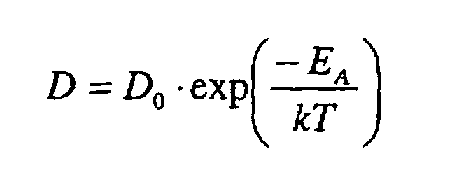
- ⁇ means here the mean way by which the Si atoms of the substrate are displaced when involved in the collision cascade. ⁇ is between 0.2 and 1.0 nm and can be accurately determined using standard programs [eg JF Ziegler (Ed.), SRIM: The Stopping and Range of Ions in Matter, Program Manual, (1996)]. For given ion dose and ion energy, q is the probability per unit time that Si atoms are misplaced in a unit volume of the substrate. q can also be calculated exactly with the standard program mentioned above. E S and E A and C 0 and D 0 are the usual material parameters for the solubility C and diffusion D of the silicon atoms in the SiO 2 layer, where C and D are described in the form of Arrhenius laws:
- the energy of the ions is chosen so that the central location at which the ions come to rest after penetrating the SiO 2 layer is sufficiently far away from the Si / SiO 2 interface in the silicon substrate.
- the ions are selected to have the same or approximately the same mass as the atoms of the silicon substrate in order to maximize the desirable effect of ion beam mixing the silicon from the surface of the silicon substrate into the SiO 2 layer, thereby reducing the ion beam dose while reducing the ion beam -induced radiation damage in the SiO 2 layer, in the silicon substrate and in possibly existing cover layers.
- the self-heating by the ion beam can be utilized for the heating of the silicon substrate and the SiO 2 layer, and thus an external substrate heating can be dispensed with.
- the SiO 2 layer may be covered by one or more layers when these layers are so thin in their entirety that the high energy ions can completely penetrate both the top layer (s) and the SiO 2 layer.
- the cover layer may be a silicon nitride layer, another chemically inert insulator layer or a metal layer chemically inert to silicon and oxygen, or a semiconducting amorphous or polycrystalline silicon layer. In the latter case, a second layer of silicon nanoclusters is produced by the ion beam mixing of the interface between the cover layer and the SiO 2 layer in the vicinity of this interface.
- the advantage of the method over the previous method of ion beam synthesis of silicon nanoclusters in SiO 2 layers is that, when the SiO 2 layer is irradiated, the highest concentration of ion-induced defects does not occur in the SiO 2 layer or in the vicinity of the SiO 2 /. Si interface, but in the so-called end-of-range (EoR) depth, far enough away from the SiO 2 / Si interface arises. Furthermore, the choice of the size of the ion energy is much less critical compared to the choice of ion energy when implanting the ions directly into the SiO 2 layer.
- the thickness of the SiO 2 layer can vary within a range of 5 to 50 nm without the ion energy having to be changed and thus having to be adapted to the specific SiO 2 layer thickness.
- Another advantage of the method over all other methods for producing Si nanocluster monolayers in SiO 2 layers is that by using the ion beam-induced substrate heating at high ion current densities and ion energies on the always necessary in all other methods and the ion beam synthesis or The deposition process following tempering can be dispensed with.
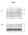
- the SiO 2 layer 1 on the silicon substrate 2 in FIG. 1 is preferably coated with silicon ions 3 having an energy of 300 keV to 800 keV and a dose of (0.1 .mu.m ) at an SiO.sub.2 layer thickness of 20 nm to 100 nm. ..10,0) ⁇ 10 16 cm -2 .
- the temperature of the SiO 2 layer during the ion irradiation is 600 to 800 ° C.
- a monolayer 4 of silicon nanoclusters is produced at a distance of 2 to 5 nm from the SiO 2 / Si interface by the ion mixing process.
- the layer 5 is located approximately where the ions come to rest (average range of the ions in the silicon substrate) and is in the present case at a depth of 0.5 microns to 1.0 microns in the silicon substrate. 2
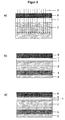
- a cover layer 6 of silicon nitride with a thickness of 100 nm is provided on the SiO 2 layer 1 with the thickness of approx. 100 nm, the energy of the silicon ions 3 is increased to 500 keV up to Increased 900 keV to fully penetrate the two layers 1 and 6.
- the layer 5 with crystal lattice damage in the silicon substrate 2 is again in a corresponding silicon substrate depth of 0.5 .mu.m to 1.0 .mu.m.
- a monolayer 7 of silicon nanoclusters is also produced in this case by the ion mixing process.
- the cover layer 8 consists of amorphous or polycrystalline silicon having a thickness of 100 nm, the ion mixing process in the vicinity of the two boundary surfaces of the SiO 2 layer 1 for the amorphous or polycrystalline silicon cover layer 8 and for the silicon substrate 2 forms a further one next to the monolayer 7 Monolayer 9 of silicon nanoclusters.
- a further modification is carried out.
- the irradiation of the SiO 2 layer 1 - here called gate oxide layer - and a polycrystalline silicon cover layer 8 - here called poly-Si gate electrode - a MOS Feldconceransistor structure is carried out with high-energy silicon ions 3.
- a layer thickness of the gate oxide of greater as 15 nm two monolayers 7 and 9 of silicon nanoclusters are produced by the ion mixing process near the two interfaces to the poly-Si gate electrode and the silicon substrate 2, respectively. If the thickness of the gate oxide layer 1 is reduced to less than 10 nm, the two monolayers 7 and 9 merge to form a monolayer 10 of silicon nanoclusters which are located approximately in the middle of the SiO 2 layer and in sufficient proximity to the SiO 2 / Si.
- the radiation of the SiO 2 layer with silicon ions with an energy of 0.7 MeV to 1.0 MeV and a Dose of (0.1 ... 10.0) x 10 16 cm -2 at a temperature of the SiO 2 layer of 600 to 800 ° C instead.
- the process step can take place with virtually unchanged process parameters even after the deposition of the poly-silicon cap layer 8, before the lithographic structuring of the two layers 1 and 8.
- the ion energy can be reduced to 500 to 700 keV.
- crystal lattice damage is also generated in the silicon substrate 2 in the situation 5.
- the layer 5 is located approximately where the silicon ions 3 are stuck in the silicon substrate 2.
Landscapes
- Chemical & Material Sciences (AREA)
- Chemical Kinetics & Catalysis (AREA)
- Engineering & Computer Science (AREA)
- Materials Engineering (AREA)
- Mechanical Engineering (AREA)
- Metallurgy (AREA)
- Organic Chemistry (AREA)
- Insulated Gate Type Field-Effect Transistor (AREA)
- Formation Of Insulating Films (AREA)
- Silicon Compounds (AREA)
- Non-Volatile Memory (AREA)
- Semiconductor Memories (AREA)
Description
Für elektrisch geladene Nanocluster in einem Dielektrikum wächst die elektrostatische Energie umgekehrt proportional mit der Clustergröße. Bei Clustergrößen von etwa 5 nm reicht daher schon die Beladung mit einem Elektron zur sicheren Informationsspeicherung bei Raumtemperatur [ S. Tawari, F. Rana, H. Hanafi, A. Hartstein, E.F. Crabbe, K. Chan, Appl. Phys. Lett. 68 (1996),1377]. Bisher ist ein gut kontrollierbares und hinreichend reproduzierbares Verfahren zur Herstellung von Nanocluster-Monolagen für höchstintegrierte Schaltkreise sowie für Einzelektronen-Transistoren nicht bekannt. Die erprobten oder sich in Untersuchung befindlichen Verfahren sind die Ionenstrahlsynthese von Nanoclustern in SiO2-Schichten, die chemische Abscheidung von Nanocluster-haltigen SiO2-Schichten aus der Dampfphase (CVD-Verfahren) und die Abscheidung derartiger Schichten durch Kathodenzerstäubung (Sputter-Verfahren).
Beim CVD-Verfahren [S. Tiwari, F. Rana, H. Hanafi, A. Hartstein, E.F. Crabbe, K. Chan, Appl. Phys. Lett., 68 (1996) 1377] wird eine SiO2-Schicht mit einer Überschußkonzentration von Silizium in einem komplizierten Mehrschrittverfahren auf ein dünnes thermisches Oxid (Tunneloxid, dox = 2...5 nm) unter Verwendung von Silan (SiH4) bei einer Temperatur von 500 bis 600 °C mit jeweils zwischenzeitlicher Oxydation zur Separation der Silizium-Cluster abgeschieden. Die Herstellung der kompletten SiO2-Schicht wird mit der Abscheidung einer dünnen amorphen Silizium-Schicht und deren Aufoxydation abgeschlossen.
Bei der Abscheidung durch Kathodenzerstäubung [H. Seifarth, R. Grötzschel, A. Markwitz, W. Matz, P. Nitzsche, L. Rebohle, Thin Solid Films, 330 (1998) 202] wird ebenfalls auf thermisch gewachsenes Tunneloxid eine 2 bis 5 nm dicke SiO2-Schicht mit einer Überschußkonzentration von Silizium und darüber anschließend eine stöchiometrische SiO2-Schicht entsprechender Dicke abgeschieden. Die Formierung der Silizium-Clusterschicht wird in einem nachfolgenden Temperschritt durchgeführt.


Bei geeigneter Wahl einer hinreichend hohen Ionenstromdichte und Ionenenergie kann für die Heizung des Siliziumsubstrates und der SiO2-Schicht die Eigenerhitzung durch den Ionenstrahl ausgenutzt werden und somit auf eine externe Substratheizung verzichtet werden.
Die SiO2-Schicht kann durch eine oder mehrere Schichten abgedeckt sein, wenn diese Schichten in ihrer Gesamtheit so dünn sind, daß die hochenergetischen Ionen sowohl die Deckschichte(n) als auch die SiO2-Schicht vollständig durchdringen können.
Die Deckschicht kann eine Siliziumnitridschicht, eine andere chemisch inerte Isolatorschicht oder eine gegenüber Silizium und Sauerstoff chemisch inerte Metallschicht oder aber eine halbleitende amorphe oder polykristalline Siliziumschicht sein. In letzterem Fall wird durch das Ionenstrahlmischen der Grenzfläche zwischen der Deckschicht und der SiO2-Schicht in Nähe dieser Grenzfläche eine zweite Lage aus Silizium-Nanoclustern erzeugt.
Ein weiterer Vorteil des Verfahrens gegenüber allen anderen Verfahren zur Herstellung von Si-Nanocluster-Monolagen in SiO2-Schichten ist, daß durch Nutzung der Ionenstrahl-induzierten Substratheizung bei hohen Ionenstromdichten und Ionenenergien auf den bei allen anderen Verfahren immer notwendigen und der Ionenstrahlsynthese bzw. den Abscheideverfahren folgenden Temperprozeß verzichtet werden kann.
- Fig. 1 a
- die Durchstrahlung einer SiO2-Schicht auf einem Siliziumsubstrat,
- Fig. 1 b
- den nach der Durchstrahlung modifizierten Schichtaufbau nach Fig. 1 a,
- Fig. 2 a
- die Durchstrahlung der mit einer Deckschicht versehenen SiO2-Schicht auf einem Siliziumsubstrat,
- Fig. 2 b
- den nach der Durchstrahlung modifizierten Schichtaufbau nach Fig. 2 a mit einer Siliziumnitrid-Deckschicht,
- Fig. 2 c
- den nach der Durchstrahlung modifizierten Schichtaufbau nach Fig. 2 a mit einer amorphen oder polykristallinen Deckschicht,
- Fig. 3 a
- die Durchstrahlung einer MOS-Feldeffekttransistor-Struktur mit einem dünnen Gateoxid und einer poly-Si-Gateelektrode,
- Fig. 3 b
- die nach der Bestrahlung modifizierte MOS-Feldeffekttransistor-Struktur mit einer Gateoxiddicke > 15 nm,
- Fig. 3 c
- die nach der Bestrahlung modifizierte MOS-Feldeffekttransistor-Struktur mit einer Gateoxiddicke < 10 nm.
Eine Modifikation des obigen Beispiels wird nachstehend beschrieben. Befindet sich - wie in Figur 2 dargestellt - auf der SiO2-Schicht 1 mit der Dicke von ca. 100 nm eine Deckschicht 6 aus Silziumnitrid mit einer Dicke von 100 nm, so wird die Energie der Silizium-Ionen 3 auf entsprechend 500 keV bis 900 keV erhöht, um die beiden Schichten 1 und 6 vollständig zu durchstrahlen. Die Lage 5 mit Kristallgitterschäden im Siliziumsubstrat 2 liegt wieder in einer entsprechenden Silizium-Substrattiefe von 0,5 µm bis 1,0 µm. In Nähe der Grenzfläche der SiO2-Schicht 1 zum Siliziumsubstrat 2 wird durch den Ionenmischprozeß auch in diesem Fall eine Monolage 7 aus Silizium-Nanoclustern erzeugt.
Besteht die Deckschicht 8 aus amorphem oder polykristallinem Silizium mit einer Dicke von 100 nm, so entsteht durch den Ionenmischprozeß in Nähe der beiden Grenzflächen der SiO2-Schicht 1 zur amorphen oder polykristallinen Silizium-Deckschicht 8 und zum Siliziumsubstrat 2 neben der Monolage 7 eine weitere Monolage 9 aus Silizium-Nanoclustern.
In den Figuren 3 ist eine weitere Modifikation ausgeführt.
Die Durchstrahlung der SiO2-Schicht 1 - hier Gateoxidschicht genannt - und einer polykristallinen Silizium-Deckschicht 8 - hier poly-Si-Gateelektrode genannt - einer MOS-Feldeffektransistor-Struktur erfolgt mit hochenergetischen Silizium-Ionen 3. Bei einer Schichtdicke des Gateoxids von größer als 15 nm werden in Nähe der beiden Grenzflächen zur poly-Si-Gateelektrode bzw. zum Siliziumsubstrat 2 zwei Monolagen 7 und 9 aus Silizium-Nanoclustern durch den Ionenmischprozeß erzeugt. Wird die Dicke der Gateoxidschicht 1 auf weniger als 10 nm reduziert, verschmelzen die beiden Monolagen 7 und 9 zu einer Monolage 10 aus Silizium-Nanoclustern, die sich ungefähr in der Mitte der SiO2-Schicht und in hinreichender Nähe zur SiO2/Si-Grenzfläche befindet.
Für MOS-Feldeffekttransistorstrukturen mit einer Gateoxiddicke von 5 nm bis 20 nm und einer Dicke der poly-Si-Gateelektrode von 300 nm findet die Durchstrahlung der SiO2-Schicht mit Siliziumionen mit einer Energie von 0,7 MeV bis 1,0 MeV und einer Dosis von (0,1...10,0)·1016 cm-2 bei einer Temperatur der SiO2-Schicht von 600 bis 800 °C statt. In Abhängigkeit von den technologischen Randbedingungen im Herstellungsprozeß von MOS-Feldeffekttransistoren kann der Verfahrensschritt mit praktisch unveränderten Prozeßparametern auch nach der Abscheidung der poly-Silizium-Deckschicht 8, noch vor der lithografischen Strukturierung der beiden Schichten 1 und 8 erfolgen. Bei Ionenbestrahlung nur der thermisch gewachsenen Gateoxid-Schicht 1 ohne Deckschicht kann die Ionenenergie auf 500 bis 700 keV reduziert werden.
Während der Ionenbestrahlung werden außerdem im Siliziumsubstrat 2 in der Lage 5 Kristallgitterschäden erzeugt. Die Lage 5 befindet sich etwa dort, wo die Silizium-Ionen 3 im Siliziumsubstrat 2 steckengeblieben sind. Die Kristallgitterschäden in der Tiefe des Siliziumsubstrats 2 können bei entsprechender Temperaturbehandlung vorhandene Verunreinigungen, besonders Schwermetalle, im Siliziumsubstrat 2 aus dem oberflächennahen Bereich des Siliziumsubstrats 2 gettern und somit die Funktionseigenschaften des MOS-Feleffekttransistorstruktur an der Oberfläche des Siliziumsubstrats 2 verbessern.
Claims (5)
- Verfahren zur Herstellung von Monolagen aus Silizium-Nanoclustern in Siliziumdioxidschichten, dadurch gekennzeichnet, daß eine wenige Nanometer bis 100 nm dicke Siliziumdioxidschicht (1) auf einem Siliziumsubstrat (2) mit Ionen (3), vorzugsweise Sauerstoff-, Silizium- oder Germaniumionen, mit einer Ionenenergie von 10 keV bis 10 MeV und einer Ionendosis von 1015 bis 1018 cm-2, bei einer Temperatur der Siliziumdioxidschicht (1) von 300 bis 800 °C durchstrahlt wird.
- Verfahren nach Anspruch 1, dadurch gekennzeichnet, daß die Siliziumdioxidschicht (1) mit Silizium-Ionen (3) durchstrahlt wird, die die gleiche atomare Masse wie die Atome des Siliziumsubstrates (2) besitzen.
- Verfahren nach Anspruch 1, dadurch gekennzeichnet, daß die Ionenbestrahlung der Siliziumdioxidschicht (1) durch eine oder mehrere darüberliegende dünne Deckschichten (6) erfolgt, wobei die Ionenenergie soweit erhöht wird, daß die Siliziumdioxidschicht (1) und die Deckschicht (6) durchstrahlt werden.
- Verfahren nach Anspruch 1 und 3, dadurch gekennzeichnet, daß bei Ionenbestrahlung von poly-Silizium- und Siliziumdioxidschichten (1) auf Siliziumsubstrat (2) die Ionenenergie bei größer oder gleich 0,5 MeV gewählt wird.
- Verfahren nach Anspruch 1, dadurch gekennzeichnet, daß die Ionenstromdichte und Ionenenergie während der Bestrahlung so gewählt werden, daß eine Ionenstrahl-induzierte Heizung des Siliziumsubstrates (2) und der Siliziumdioxidschicht (1) von 300 bis 800 °C erreicht wird.
Applications Claiming Priority (2)
| Application Number | Priority Date | Filing Date | Title |
|---|---|---|---|
| DE19933632A DE19933632C2 (de) | 1999-07-17 | 1999-07-17 | Verfahren zur Herstellung von Monolagen aus Silizium-Nanoclustern in Siliziumdioxid |
| DE19933632 | 1999-07-17 |
Publications (2)
| Publication Number | Publication Date |
|---|---|
| EP1070768A1 EP1070768A1 (de) | 2001-01-24 |
| EP1070768B1 true EP1070768B1 (de) | 2005-05-04 |
Family
ID=7915170
Family Applications (1)
| Application Number | Title | Priority Date | Filing Date |
|---|---|---|---|
| EP00114817A Expired - Lifetime EP1070768B1 (de) | 1999-07-17 | 2000-07-11 | Verfahren zur Herstellung von Monolagen aus Silizium-Nanoclustern in Siliziumdioxid |
Country Status (3)
| Country | Link |
|---|---|
| EP (1) | EP1070768B1 (de) |
| AT (1) | ATE294878T1 (de) |
| DE (2) | DE19933632C2 (de) |
Families Citing this family (3)
| Publication number | Priority date | Publication date | Assignee | Title |
|---|---|---|---|---|
| EP1389799A1 (de) * | 2002-08-13 | 2004-02-18 | Aarhus University | Verfahren zur Herstellung von Schichtstrukturen mit Nanokristalliten in einer dielektrischen Schicht |
| RU2214359C1 (ru) * | 2002-09-05 | 2003-10-20 | Санкт-Петербургский государственный институт точной механики и оптики (технический университет) | Способ формирования решетки нанокластеров кремния на структурированной подложке |
| RU2292606C2 (ru) * | 2004-12-14 | 2007-01-27 | Институт микроэлектроники и информатики РАН | Способ получения квантоворазмерных структур на основе аморфных кремниевых нанокластеров, встроенных в диэлектрическую матрицу |
Family Cites Families (1)
| Publication number | Priority date | Publication date | Assignee | Title |
|---|---|---|---|---|
| JPH0750693B2 (ja) * | 1985-12-02 | 1995-05-31 | 日本テキサス・インスツルメンツ株式会社 | 酸化シリコン膜の製造方法 |
-
1999
- 1999-07-17 DE DE19933632A patent/DE19933632C2/de not_active Expired - Fee Related
-
2000
- 2000-07-11 DE DE50010207T patent/DE50010207D1/de not_active Expired - Lifetime
- 2000-07-11 EP EP00114817A patent/EP1070768B1/de not_active Expired - Lifetime
- 2000-07-11 AT AT00114817T patent/ATE294878T1/de not_active IP Right Cessation
Also Published As
| Publication number | Publication date |
|---|---|
| DE50010207D1 (de) | 2005-06-09 |
| DE19933632A1 (de) | 2001-01-18 |
| EP1070768A1 (de) | 2001-01-24 |
| DE19933632C2 (de) | 2002-11-21 |
| ATE294878T1 (de) | 2005-05-15 |
Similar Documents
| Publication | Publication Date | Title |
|---|---|---|
| DE69133183T2 (de) | Silizium auf porösen silizium, verfahren zur herstellung und produkt | |
| DE60130205T2 (de) | Implantierungsverfahren unter verwendung substöchiometrischer sauerstoffdosen bei verschiedenen energien | |
| DE68919561T2 (de) | Verfahren zur Oberflächenpassivierung eines zusammengesetzten Halbleiters. | |
| DE4226888C2 (de) | Diamant-Feldeffekt-Transistor und Verfahren zu dessen Herstellung | |
| DE3311635A1 (de) | Halbleiterbauelement und verfahren zu dessen herstellung | |
| DE19627017A1 (de) | Verfahren zur selektiven Ablagerung eines Metallfilms | |
| DE10034942A1 (de) | Verfahren zur Erzeugung eines dotierten Halbleitersubstrats | |
| DE4229628A1 (de) | Halbleitereinrichtung vom stapeltyp und verfahren zur herstellung einer solchen | |
| DE2845460A1 (de) | Verfahren zur herstellung einer halbleitervorrichtung | |
| DE69033879T2 (de) | Herstellung eines elektronischen Bauteiles unter Verwendung eines Schrittes zur Strukturerzeugung | |
| DE102014210406B4 (de) | Verfahren zur Herstellung eines Transistors mit einem verspannten Kanalgebiet | |
| DE69432604T2 (de) | Verfahren für die herstellung eines halbleitersubstrates | |
| DE102015102225A1 (de) | Verfahren zur Verarbeitung einer Schicht und Verfahren zur Herstellung einer elektronischen Vorrichtung | |
| DE112015000137T5 (de) | Verfahren zum Herstellen einer Halbleitervorrichtung | |
| DE4313042C2 (de) | Diamantschichten mit hitzebeständigen Ohmschen Elektroden und Herstellungsverfahren dafür | |
| DE102014107105A1 (de) | Verfahren zur verarbeitung eines trägers und eine elektronische komponente | |
| DE69720441T2 (de) | Bauelement mit gesteuerter Leitung | |
| DE102004031453B4 (de) | Verfahren zur Erzeugung eines Dielektrikums und Halbleiterstruktur | |
| DE102013205068B4 (de) | Verfahren zur Herstellung eines Gatedielektrikums einer Gateelektrode | |
| DE69800026T2 (de) | GaAs-basierender MOSFET und Verfahren zur Herstellung | |
| DE102016122217B4 (de) | Verfahren zum dünnen von substraten | |
| DE102009046241B4 (de) | Verformungsverstärkung in Transistoren, die eine eingebettete verformungsinduzierende Halbleiterlegierung besitzen, durch Kantenverrundung an der Oberseite der Gateelektrode | |
| DE19933632C2 (de) | Verfahren zur Herstellung von Monolagen aus Silizium-Nanoclustern in Siliziumdioxid | |
| DE10350354A1 (de) | Orientierungs-unabhängige Oxidation von nitriertem Silizium | |
| DE10214065B4 (de) | Verfahren zur Herstellung eines verbesserten Metallsilizidbereichs in einem Silizium enthaltenden leitenden Gebiet in einer integrierten Schaltung |
Legal Events
| Date | Code | Title | Description |
|---|---|---|---|
| PUAI | Public reference made under article 153(3) epc to a published international application that has entered the european phase |
Free format text: ORIGINAL CODE: 0009012 |
|
| AK | Designated contracting states |
Kind code of ref document: A1 Designated state(s): AT BE CH CY DE DK ES FI FR GB GR IE IT LI LU MC NL PT SE |
|
| AX | Request for extension of the european patent |
Free format text: AL;LT;LV;MK;RO;SI |
|
| 17P | Request for examination filed |
Effective date: 20010504 |
|
| AKX | Designation fees paid |
Free format text: AT BE CH CY DE DK ES FI FR GB GR IE IT LI LU MC NL PT SE |
|
| RAP1 | Party data changed (applicant data changed or rights of an application transferred) |
Owner name: FORSCHUNGSZENTRUM ROSSENDORF E.V. |
|
| GRAP | Despatch of communication of intention to grant a patent |
Free format text: ORIGINAL CODE: EPIDOSNIGR1 |
|
| GRAS | Grant fee paid |
Free format text: ORIGINAL CODE: EPIDOSNIGR3 |
|
| GRAA | (expected) grant |
Free format text: ORIGINAL CODE: 0009210 |
|
| AK | Designated contracting states |
Kind code of ref document: B1 Designated state(s): AT BE CH CY DE DK ES FI FR GB GR IE IT LI LU MC NL PT SE |
|
| PG25 | Lapsed in a contracting state [announced via postgrant information from national office to epo] |
Ref country code: IT Free format text: LAPSE BECAUSE OF FAILURE TO SUBMIT A TRANSLATION OF THE DESCRIPTION OR TO PAY THE FEE WITHIN THE PRESCRIBED TIME-LIMIT;WARNING: LAPSES OF ITALIAN PATENTS WITH EFFECTIVE DATE BEFORE 2007 MAY HAVE OCCURRED AT ANY TIME BEFORE 2007. THE CORRECT EFFECTIVE DATE MAY BE DIFFERENT FROM THE ONE RECORDED. Effective date: 20050504 Ref country code: IE Free format text: LAPSE BECAUSE OF FAILURE TO SUBMIT A TRANSLATION OF THE DESCRIPTION OR TO PAY THE FEE WITHIN THE PRESCRIBED TIME-LIMIT Effective date: 20050504 Ref country code: NL Free format text: LAPSE BECAUSE OF FAILURE TO SUBMIT A TRANSLATION OF THE DESCRIPTION OR TO PAY THE FEE WITHIN THE PRESCRIBED TIME-LIMIT Effective date: 20050504 Ref country code: GB Free format text: LAPSE BECAUSE OF FAILURE TO SUBMIT A TRANSLATION OF THE DESCRIPTION OR TO PAY THE FEE WITHIN THE PRESCRIBED TIME-LIMIT Effective date: 20050504 Ref country code: FI Free format text: LAPSE BECAUSE OF FAILURE TO SUBMIT A TRANSLATION OF THE DESCRIPTION OR TO PAY THE FEE WITHIN THE PRESCRIBED TIME-LIMIT Effective date: 20050504 |
|
| REG | Reference to a national code |
Ref country code: GB Ref legal event code: FG4D Free format text: NOT ENGLISH |
|
| REG | Reference to a national code |
Ref country code: CH Ref legal event code: EP |
|
| REG | Reference to a national code |
Ref country code: IE Ref legal event code: FG4D Free format text: LANGUAGE OF EP DOCUMENT: GERMAN |
|
| REF | Corresponds to: |
Ref document number: 50010207 Country of ref document: DE Date of ref document: 20050609 Kind code of ref document: P |
|
| PG25 | Lapsed in a contracting state [announced via postgrant information from national office to epo] |
Ref country code: AT Free format text: LAPSE BECAUSE OF NON-PAYMENT OF DUE FEES Effective date: 20050711 Ref country code: CY Free format text: LAPSE BECAUSE OF FAILURE TO SUBMIT A TRANSLATION OF THE DESCRIPTION OR TO PAY THE FEE WITHIN THE PRESCRIBED TIME-LIMIT Effective date: 20050711 Ref country code: LU Free format text: LAPSE BECAUSE OF NON-PAYMENT OF DUE FEES Effective date: 20050711 |
|
| PG25 | Lapsed in a contracting state [announced via postgrant information from national office to epo] |
Ref country code: LI Free format text: LAPSE BECAUSE OF NON-PAYMENT OF DUE FEES Effective date: 20050731 Ref country code: MC Free format text: LAPSE BECAUSE OF NON-PAYMENT OF DUE FEES Effective date: 20050731 Ref country code: BE Free format text: LAPSE BECAUSE OF NON-PAYMENT OF DUE FEES Effective date: 20050731 Ref country code: CH Free format text: LAPSE BECAUSE OF NON-PAYMENT OF DUE FEES Effective date: 20050731 |
|
| PG25 | Lapsed in a contracting state [announced via postgrant information from national office to epo] |
Ref country code: SE Free format text: LAPSE BECAUSE OF FAILURE TO SUBMIT A TRANSLATION OF THE DESCRIPTION OR TO PAY THE FEE WITHIN THE PRESCRIBED TIME-LIMIT Effective date: 20050804 Ref country code: GR Free format text: LAPSE BECAUSE OF FAILURE TO SUBMIT A TRANSLATION OF THE DESCRIPTION OR TO PAY THE FEE WITHIN THE PRESCRIBED TIME-LIMIT Effective date: 20050804 Ref country code: DK Free format text: LAPSE BECAUSE OF FAILURE TO SUBMIT A TRANSLATION OF THE DESCRIPTION OR TO PAY THE FEE WITHIN THE PRESCRIBED TIME-LIMIT Effective date: 20050804 |
|
| PG25 | Lapsed in a contracting state [announced via postgrant information from national office to epo] |
Ref country code: ES Free format text: LAPSE BECAUSE OF FAILURE TO SUBMIT A TRANSLATION OF THE DESCRIPTION OR TO PAY THE FEE WITHIN THE PRESCRIBED TIME-LIMIT Effective date: 20050815 |
|
| PG25 | Lapsed in a contracting state [announced via postgrant information from national office to epo] |
Ref country code: PT Free format text: LAPSE BECAUSE OF FAILURE TO SUBMIT A TRANSLATION OF THE DESCRIPTION OR TO PAY THE FEE WITHIN THE PRESCRIBED TIME-LIMIT Effective date: 20051017 |
|
| NLV1 | Nl: lapsed or annulled due to failure to fulfill the requirements of art. 29p and 29m of the patents act | ||
| GBV | Gb: ep patent (uk) treated as always having been void in accordance with gb section 77(7)/1977 [no translation filed] |
Effective date: 20050504 |
|
| REG | Reference to a national code |
Ref country code: IE Ref legal event code: FD4D |
|
| PLBE | No opposition filed within time limit |
Free format text: ORIGINAL CODE: 0009261 |
|
| STAA | Information on the status of an ep patent application or granted ep patent |
Free format text: STATUS: NO OPPOSITION FILED WITHIN TIME LIMIT |
|
| REG | Reference to a national code |
Ref country code: CH Ref legal event code: PL |
|
| 26N | No opposition filed |
Effective date: 20060207 |
|
| EN | Fr: translation not filed | ||
| BERE | Be: lapsed |
Owner name: FORSCHUNGSZENTRUM ROSSENDORF E.V. Effective date: 20050731 |
|
| PG25 | Lapsed in a contracting state [announced via postgrant information from national office to epo] |
Ref country code: FR Free format text: LAPSE BECAUSE OF NON-PAYMENT OF DUE FEES Effective date: 20050731 |
|
| PG25 | Lapsed in a contracting state [announced via postgrant information from national office to epo] |
Ref country code: FR Free format text: LAPSE BECAUSE OF NON-PAYMENT OF DUE FEES Effective date: 20050504 |
|
| PGFP | Annual fee paid to national office [announced via postgrant information from national office to epo] |
Ref country code: DE Payment date: 20110719 Year of fee payment: 12 |
|
| PG25 | Lapsed in a contracting state [announced via postgrant information from national office to epo] |
Ref country code: DE Free format text: LAPSE BECAUSE OF NON-PAYMENT OF DUE FEES Effective date: 20130201 |
|
| REG | Reference to a national code |
Ref country code: DE Ref legal event code: R119 Ref document number: 50010207 Country of ref document: DE Effective date: 20130201 |