EP1069655A2 - Connecteur électrique à diaphonie réduite - Google Patents
Connecteur électrique à diaphonie réduite Download PDFInfo
- Publication number
- EP1069655A2 EP1069655A2 EP00114190A EP00114190A EP1069655A2 EP 1069655 A2 EP1069655 A2 EP 1069655A2 EP 00114190 A EP00114190 A EP 00114190A EP 00114190 A EP00114190 A EP 00114190A EP 1069655 A2 EP1069655 A2 EP 1069655A2
- Authority
- EP
- European Patent Office
- Prior art keywords
- talk
- cross
- trace
- layer
- compensating
- Prior art date
- Legal status (The legal status is an assumption and is not a legal conclusion. Google has not performed a legal analysis and makes no representation as to the accuracy of the status listed.)
- Withdrawn
Links
Images


Classifications
-
- H—ELECTRICITY
- H01—ELECTRIC ELEMENTS
- H01R—ELECTRICALLY-CONDUCTIVE CONNECTIONS; STRUCTURAL ASSOCIATIONS OF A PLURALITY OF MUTUALLY-INSULATED ELECTRICAL CONNECTING ELEMENTS; COUPLING DEVICES; CURRENT COLLECTORS
- H01R13/00—Details of coupling devices of the kinds covered by groups H01R12/70 or H01R24/00 - H01R33/00
- H01R13/46—Bases; Cases
- H01R13/514—Bases; Cases composed as a modular blocks or assembly, i.e. composed of co-operating parts provided with contact members or holding contact members between them
-
- H—ELECTRICITY
- H05—ELECTRIC TECHNIQUES NOT OTHERWISE PROVIDED FOR
- H05K—PRINTED CIRCUITS; CASINGS OR CONSTRUCTIONAL DETAILS OF ELECTRIC APPARATUS; MANUFACTURE OF ASSEMBLAGES OF ELECTRICAL COMPONENTS
- H05K1/00—Printed circuits
- H05K1/02—Details
- H05K1/0213—Electrical arrangements not otherwise provided for
- H05K1/0216—Reduction of cross-talk, noise or electromagnetic interference
- H05K1/0228—Compensation of cross-talk by a mutually correlated lay-out of printed circuit traces, e.g. for compensation of cross-talk in mounted connectors
-
- H—ELECTRICITY
- H01—ELECTRIC ELEMENTS
- H01R—ELECTRICALLY-CONDUCTIVE CONNECTIONS; STRUCTURAL ASSOCIATIONS OF A PLURALITY OF MUTUALLY-INSULATED ELECTRICAL CONNECTING ELEMENTS; COUPLING DEVICES; CURRENT COLLECTORS
- H01R13/00—Details of coupling devices of the kinds covered by groups H01R12/70 or H01R24/00 - H01R33/00
- H01R13/646—Details of coupling devices of the kinds covered by groups H01R12/70 or H01R24/00 - H01R33/00 specially adapted for high-frequency, e.g. structures providing an impedance match or phase match
- H01R13/6461—Means for preventing cross-talk
- H01R13/6464—Means for preventing cross-talk by adding capacitive elements
- H01R13/6466—Means for preventing cross-talk by adding capacitive elements on substrates, e.g. printed circuit boards [PCB]
-
- H—ELECTRICITY
- H01—ELECTRIC ELEMENTS
- H01R—ELECTRICALLY-CONDUCTIVE CONNECTIONS; STRUCTURAL ASSOCIATIONS OF A PLURALITY OF MUTUALLY-INSULATED ELECTRICAL CONNECTING ELEMENTS; COUPLING DEVICES; CURRENT COLLECTORS
- H01R13/00—Details of coupling devices of the kinds covered by groups H01R12/70 or H01R24/00 - H01R33/00
- H01R13/646—Details of coupling devices of the kinds covered by groups H01R12/70 or H01R24/00 - H01R33/00 specially adapted for high-frequency, e.g. structures providing an impedance match or phase match
- H01R13/6473—Impedance matching
- H01R13/6474—Impedance matching by variation of conductive properties, e.g. by dimension variations
-
- H—ELECTRICITY
- H05—ELECTRIC TECHNIQUES NOT OTHERWISE PROVIDED FOR
- H05K—PRINTED CIRCUITS; CASINGS OR CONSTRUCTIONAL DETAILS OF ELECTRIC APPARATUS; MANUFACTURE OF ASSEMBLAGES OF ELECTRICAL COMPONENTS
- H05K1/00—Printed circuits
- H05K1/16—Printed circuits incorporating printed electric components, e.g. printed resistors, capacitors or inductors
- H05K1/162—Printed circuits incorporating printed electric components, e.g. printed resistors, capacitors or inductors incorporating printed capacitors
-
- H—ELECTRICITY
- H05—ELECTRIC TECHNIQUES NOT OTHERWISE PROVIDED FOR
- H05K—PRINTED CIRCUITS; CASINGS OR CONSTRUCTIONAL DETAILS OF ELECTRIC APPARATUS; MANUFACTURE OF ASSEMBLAGES OF ELECTRICAL COMPONENTS
- H05K2201/00—Indexing scheme relating to printed circuits covered by H05K1/00
- H05K2201/09—Shape and layout
- H05K2201/09209—Shape and layout details of conductors
- H05K2201/09218—Conductive traces
- H05K2201/09236—Parallel layout
-
- H—ELECTRICITY
- H05—ELECTRIC TECHNIQUES NOT OTHERWISE PROVIDED FOR
- H05K—PRINTED CIRCUITS; CASINGS OR CONSTRUCTIONAL DETAILS OF ELECTRIC APPARATUS; MANUFACTURE OF ASSEMBLAGES OF ELECTRICAL COMPONENTS
- H05K2201/00—Indexing scheme relating to printed circuits covered by H05K1/00
- H05K2201/10—Details of components or other objects attached to or integrated in a printed circuit board
- H05K2201/10007—Types of components
- H05K2201/10189—Non-printed connector
Definitions
- the present invention relates to electrical connector systems. More specifically, the present invention relates to electrical connector systems that minimize cross-talk.
- Cross-talk occurs when electromagnetic energy transmitted through a conductor in the connector causes electrical currents in the another conductor in the electrical connector.
- Near-end cross-talk travels in a direction opposite to the signal in the conductor.
- ANSI/EIA/TIA/568A Category 5 requirements limit pair-to-pair NEXT to -40 dB at 100 MHz.
- U.S. Patent number 5,562,479 describes an electrical connector in which a mating portion of the connector produces a "positive" cross-talk. Another portion of the connector arranges the conductors side-by-side in a plane to produce a "negative” cross-talk. The "negative" cross-talk cancels out the "positive" cross-talk.
- U.S. Patent number 5,647,770 describes a modular jack in which adjacent conductor wires are crossed over for a portion of a length along an insert. The cross-talk produced in the cross-over portion cancels out the cross-talk produced in the portions of the conductor wire that are not crossed-over.
- British Patent Application GB 2 314 466 describes a compensation pattern on a multi-layer board (MLB) to which contacts from an electrical connector secure.
- the pattern uses vertically aligned arrays of conductive paths. Capacitive coupling between adjacent unlike paths produces a cross-talk that reduces the cross-talk produced by the connector.
- the pattern also staggers adjacent paths on a layer in order to allow coupling between non-adjacent paths.
- European Patent Application number EP 0 854 664 also describes a compensation pattern on an MLB to which the electrical connector contacts connect. A portion of the conductive paths extend along one layer, while the remainder extends along another layer vertically spaced therefrom. The arrangement of the paths ensures that one path of a pair overlies at least two paths, each from a different pair.
- an electrical connector system comprising: an electrical connector having a plurality of signal contacts and in which the signal contacts exhibit unwanted cross-talk; and a circuit substrate engaging said connector.
- the substrate has a plurality of layers; and at least first, second and third traces on the circuit substrate, each corresponding to a respective signal contact.
- the first trace includes: a first portion on at least one of the plurality of layers and adjacent a portion of the second trace in order to produce a first compensating cross-talk; a second portion on at least one other of the plurality of layers and adjacent a portion of the third trace in order to produce a second compensating cross-talk.
- the first and second compensating cross-talks offset the unwanted cross-talk to provide an acceptable cross-talk.
- a circuit substrate for creating compensating cross-talk that minimizes unwanted cross-talk in signal contacts of an electrical connector.
- the substrate comprises a board having a first layer, a second layer, a plurality of inner layers between said first and second layers, and a ground plane on at least a lower surface of said board; at least first, second and third traces on the inner layers, the first trace having portions adjacent the second and third traces in order to produce a first and a second compensating cross-talk, respectively.
- the first and second compensating cross-talks offset the unwanted cross-talk to produce an acceptable cross-talk.
- a method of reducing unwanted cross-talk in an array of at least three conductors comprising the steps of: introducing a first compensating cross-talk by inductively and capacitively coupling a first conductor and a second conductor adjacent the first conductor; and introducing a second compensating cross-talk by capacitively coupling the first conductor and a third conductor once removed from the first conductor.
- the compensating cross-talks offset the unwanted cross-talk to produce an acceptable cross-talk.
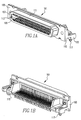
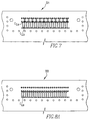
- FIGS 1A and 1B display an electrical connector 101, which could be a Category 5, 25 pair PCB receptacle connector such as part number 92509 available from FCI. Since a detailed recitation of the features of receptacle 101 is unnecessary for an understanding of the present invention, only a brief summary follows.
- Receptacle 101 has an insulative housing 103 made from a suitable material such as 40% glass fiber reinforced polyphenylene sulfide (PPS).
- a series of contacts 105 extend through housing 103.
- Contacts 105 can be made from any suitable conductive material, including phosphor-bronze, with a suitable plating finish, such as gold over nickel.
- Receptacle 101 includes a mating portion 107 extending from a front face 109.
- a metal shell 111 covers front face 109 and surrounds the perimeter of mating portion 107.
- Mating portion 107 has a central opening 113 that accepts a mating electrical connector therein.
- contacts 105 reside within mating portion 107 in two opposed rows.
- the mating ends of contacts 105 could be cantilever beams or propped cantilever beams which engage contacts in the mating electrical connector.
- superimposed contacts 105a, 105b within mating portion 107 define the differential pairs.
- Contacts 105 extend past a mounting portion 115 of receptacle 101, for example, to engage through holes in a circuit substrate.
- the tails of contacts 105 extend from receptacle 101 in two rows.
- Mounting portion 113 could also include hold downs 117 that engage through holes in the circuit substrate to secure receptacle 101 temporarily to the circuit substrate before soldering.
- receptacle 101 could also have an outer shield 119 to shield any electrical components surrounding receptacle 101 from electromagnetic interference (EMI) which could induce common mode noise in the cable.
- Shield 119 is preferably formed from a sheet of conductive material, such as phosphor bronze with a hot dip tin finish. Aside from an opening 121 through which mating portion 107 and shell 111 extend and the side abuts the circuit substrate, shield 119 surrounds receptacle 101.
- Shield 119 can include terminals 123 that enter through holes in the circuit substrate.
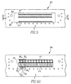
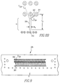
- Receptacle 101 mates with a suitable electrical connector, such as a Category 5, 25 pair cable plug 201 shown in Figures 3A and 3B.
- Plug 201 could, for example, be part number 86005 available from FCI.
- receptacle 101 a detailed recitation of the features of plug 201 is unnecessary for an understanding of the present invention. Thus, only a brief summary follows.
- Plug 201 includes a cable 203 that terminates within a housing 205 made from a suitable insulative material, such as a thermoplastic.
- Housing 205 has a plate 207 extending from a mating face 209. Plate 209 enters opening 113 in mating portion 107 of receptacle 101 during mating.
- a plurality contacts 211 extend through housing 205.
- Contacts 211 are preferably phosphor bronze with a gold over nickel finish in the contact area and a tin-lead over nickel finish in the terminal area.
- each contact 211 terminates to a respective wire 213 in the cable 203.
- the mating ends of each contact 213 extends along plate 207.
- the mating ends of contacts 213 are arranged in two rows, each on an opposite side of plate 207.
- superimposed contacts 211a, 211b extending from housing 205 define the differential pairs.
- cross-talk occurs between conductors in receptacle 101 and plug 201 (hereinafter referred to as unwanted cross-talk).
- the present invention introduces a cross-talk (hereinafter referred to as a compensating cross-talk) to each differential pair of the electrical connector system in order to reduce, or even cancel, the unwanted cross-talk.
- the present invention uses a predetermined pattern of traces on a portion of a multi-layer circuit substrate to introduce the compensating cross-talk.
- the compensating cross-talk described throughout may be in addition to any compensating cross-talk introducing within the connectors (not shown).
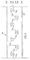
- FIGs 4-9 demonstrate a first alternative embodiment of a circuit substrate to which receptacle 101 mounts.
- the circuit substrate is made from a suitable dielectric material, such as a glass reinforced epoxy resin like FR4.
- the substrate comprises a plurality of layers formed by conventional techniques and sandwiched together by, for example, adhesive.
- multi-layer board (MLB) 301 should include at least 6 conductor layers.
- Figure 5 displays an upper surface 303 of MLB 301, which is a part of a first layer 305.
- Receptacle 101 mounts to upper surface 303 of MLB 301.
- first layer 303 has plated through holes 307, 309 which correspond to and receive terminals 123 of shield 119 and hold downs 117 of receptacle 101, respectively, and which connect terminals 123 and hold downs 117 to the ground planes of MLB 301.
- First layer 303 also includes plated through holes 311 that receive the tails of contacts 105 of receptacle 101 and vias 313 to which the other circuitry (not shown) on MLB 301 are routed. In one possible arrangement and as shown in Figure 5, through holes 311 could be arranged in two rows, while vias 313 are arranged in a single row. Other arrangements, however, are possible.
- first layer 303 could be a ground plane as illustrated in Figure 5.
- a sixth layer 317 also preferably has a ground plane at locations other than those locations necessary for creating a clearance with a plated through hole carrying a signal.
- Sixth layer 317 is preferably a lower surface 315 of MLB 301. If more than six layers were necessary, then the additional areas would reside between first and sixth layers 303, 317. In a preferred embodiment, a 0.030" spacing exists between the ground plane on sixth layer 317 and the conductors on the fifth layer. As discussed above, should MLB 301 require more than six layers, the spacing between the conductors on the fifth layer and the ground plane on sixth layer 317 would be greater.
- a predetermined arrangement of conductive paths extending between through holes 311 and vias 313 and on the various layers of MLB 301 to form the compensation pattern used to offset the unwanted cross-talk is formed on the layers using conventional techniques such as photolithography.
- each differential pair of conductors DP n comprises two conductors C n,a and C n,b .
- Figure 6A shows that a first differential pair DP 1 has a first conductor C 1,a and a second conductor C 1,b .
- a second layer 319 and an adjacent third layer 321 are preferably used to create a compensating cross-talk that offsets unwanted cross-talk between adjacent conductors.
- first layer 303 maintains a distance of approximately 0.030" from the conductors on second layer 319.
- Second and third layers 319, 321 preferably utilize inductive and capacitive coupling between adjacent differential pairs DP n , DP n+1 to create the compensating cross-talk.
- Inductive coupling occurs because the conductors carry current between through holes 311 and vias 313.
- conductors from adjacent differential pairs reside on alternating layers.
- Figure 6A displays second layer 319 having conductors thereon from a first differential pair DP 1 , a third differential pair DP 3 and a fifth differential pair DP 5 .
- Figure 7 displays third layer 321 having conductors thereon from a second differential pair DP 2 and a fourth differential pair DP 4 .
- conductors on second and third layer 319, 321 are vertically spaced approximately 0.005".
- each conductor of alternating differential pairs extend from through hole 311 to via 313 on second layer 319.
- conductor C 3,a includes a longitudinally extending portion 323 flanked by laterally extending portions 325, 327. Lateral portions 325, 327 ensure that longitudinal portion 323 generally extends to via 313 from a location generally between adjacent through holes 311.
- Conductor C 3,b includes a laterally extending portion 329 and a longitudinally extending portion 331.
- Lateral portion 329 ensures that longitudinal portion 331 generally extends to via 313 from a location generally between adjacent through holes, but on an opposite side of through hole 311 from conductor C 3,a .
- Third layer 321 has the same conductor pattern as second layer 319.
- the only difference between third layer 321 and second layer 319 is that each layer accommodates different differential pairs.
- Figure 7 shows, for example, that conductors C 2,a and C 2,b on third layer 321 follow the same pattern as conductors C 3,a and C 3,b on second layer 319.
- lateral portions 325, 327, 329 also position longitudinal portions 323, 331 relative to the longitudinal portions of the conductors on third layer 321.
- an overlap O occurs between certain conductors on second layer 319 and third layer 321. This overlap O creates the compensating cross-talk to offset unwanted cross-talk between adjacent pairs ( e.g . DP n , DP n+1 ).
- the geometry of the conductors and the spacing between second layer 319 and third layer 321 determines the amount of compensating cross-talk.
- Each conductor on second and third layer 319, 321 has a narrow interconnection portion and a wide compensation portion. The compensation discussed herein generally occurs in the wide portion of the conductors.
- Figure 6B demonstrates that lateral portion 325 of conductor C 3,a forms the narrow portion arid longitudinal portion 323 and lateral portion 327 form the wide portions.
- Figure 6B also demonstrates that lateral portion 329 and a portion of longitudinal portion 331 of conductor C 3,b form the narrow portion and the remainder of longitudinal portion 331 forms the wide portion.
- the wide portions of the conductors occupy the overlaps O with the conductors on the adjacent layer of MLB 301.
- Width W of the wide portions of the conductors is selected to produce the desired amount of compensating cross-talk.
- the width W suitable to form the desired amount of compensating cross-talk depends upon a length L between through holes 311 and vias 313. Generally speaking, for wider widths W, the optimum length L is shorter, but the resulting power sum cross-talk is larger.
- a 0.001" thick conductor should have a wide portion width of 0.016".
- the narrow portion width could be approximately 0.008".
- Subsequent layers of MLB 301 are preferably used to create a compensating cross-talk that offsets unwanted cross-talk between non-adjacent conductors.
- the remaining layers preferably use capacitive coupling between non-adjacent differential pairs to create the compensating cross-talk.
- the conductors of the subsequent layers are spaced approximately 0.011" from the conductors in third layer 321.
- Figure 6A shows that third differential pair DP 3 is "once removed" from first differential pair DP 1 .
- second differential pair DP 2 resides between first differential pair DP 1 and third differential pair DP 3 .
- fourth differential pair DP 4 is "twice removed” from differential pair DP 1 .
- second and third differential pairs DP 2 , DP 3 reside between first differential pair DP 1 and fourth differential pair DP 4 .
- a fourth layer 333 and an adjacent fifth layer 335 create a compensating cross-talk to offset unwanted cross-talk between once removed conductors.
- each conductor C n,a , C n,b from a differential pair DP n reside on alternating layers.
- Figure 8A displays fourth layer 333 having conductor C 3,a from differential pair DP 3 .
- the other conductor C 3,b from differential pair DP 3 resides on fifth layer 335.
- conductors on fourth and fifth layer 333, 335 are vertically spaced approximately 0.005".
- conductor C 3,a is a stub, not fully extending between through hole 311 and via 313.
- Conductor C 3,a has a laterally extending portion 337 and a longitudinally extending portion 339. Laterally extending portion 337 aligns longitudinal portion 339 with an adjacent via 313.
- Fifth layer 335 has a somewhat similar arrangement.
- conductor C 2,b is a stub, not fully extending between through hole 311 and via 313.
- Conductor C 2,b has a laterally extending portion 341 and a longitudinally extending portion 343.
- Laterally extending portion 341 aligns longitudinal portion 343 with an adjacent via 313.
- lateral portions 337, 341 position their respective longitudinal portions 339, 343 so as to overlap O. This overlap creates the compensating cross-talk to offset unwanted cross-talk between once removed pairs ( e.g . DP n , DP n+2 ).
- Each conductor on fourth and fifth layers 333, 335 has a narrow portion and a wide portion.
- Figures 8A and 9 demonstrate that lateral portions 337, 341 of conductors C 3,a , C 2,b form the narrow portions and longitudinal portions 339, 343 form the wide portions.
- Width W s of the wide portions of the conductors is selected to form the desired amount of compensating cross-talk.
- the width W s suitable to form the desired amount of compensating cross-talk depends upon a stub length L s .
- width W should be smaller.
- a 0.001" thick conductor with a stub length L s of 0.249" should have a wide portion width of 0.016".
- the narrow portion width could be approximately 0.008".
- Figures 10-12 display a second alternative embodiment of a circuit substrate to which receptacle 101 mounts.
- the substrate comprises a plurality of layers.
- a multi-layer board (MLB) 401 of the second alternative embodiment has at least two more layers.
- MLB 401 has a first layer 405, second layer 419, third layer 421, fourth layer 433 and fifth layer 435.
- First layer 405 includes an upper surface of MLB 401 and interacts with receptacle 101.
- Second and third layers 419, 421 create a compensating cross-talk between adjacent conductors (such as second and third differential pairs DP 2 , DP 3 ).
- Fourth and fifth layers 433, 435 create a compensating cross-talk between once removed conductors (such as second and fourth differential pairs DP 2 , DP 4 ).
- MLB 401 includes at least two additional layers that create compensating cross-talk in the conductors.
- MLB 401 includes a sixth layer 445 and an adjacent seventh layer 447.
- conductors on sixth and seventh layers 445, 447 are vertically spaced approximately 0.005".
- First layer 405 and an eighth layer 449 flank second, third, fourth, fifth, sixth and seventh layers 419, 421, 433, 435, 445, 447.
- first and eighth layers 405, 449 comprise ground planes.
- no ground plane may be necessary on first layer 405 in the region of the compensation pattern should receptacle 101 include shield 119.
- Sixth and seventh layers 445, 447 preferably create a compensating cross-talk that offsets unwanted cross-talk between twice removed conductors.
- each conductor C n,a , C n,b from a differential pair DP n resides on alternating layers.
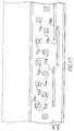
- Figure 11A displays sixth layer 445 having conductor C 13,b from thirteenth differential pair DP 13 .
- the other conductor C 13,a from thirteenth differential pair DP 13 resides on seventh layer 447.
- conductor C 13,b is a stub, not fully extending between the rows of through holes 411.
- Conductor C 13,b extends diagonally from through hole 411 associated with thirteenth differential pair DP 13 towards through hole 411 associated with a sixteenth differential pair DP 16 .
- Seventh layer 447 has a similar arrangement.
- conductor C 16,a is a stub, not fully extending between the rows of through holes 411.
- Conductor C 16,a extends diagonally from through hole 411 associated with sixteenth differential pair DP 16 towards through hole 411 associated with a thirteenth differential pair DP 13 .
- the positioning of the conductors provides an overlap O between twice removed conductors as seen in Figure 11B. This overlap O creates the compensating cross-talk to offset the unwanted cross-talk between twice removed pairs ( e.g . DP n , DP n+3 ).
- the geometry of the conductors and the spacing between the sixth and seventh layers 445, 447 determines the amount of compensating cross-talk.
- Each conductor on sixth and seventh layers 445, 447 preferably has a generally uniform width.
- the width of the conductors is selected to form the desired amount of compensating cross-talk.
- the width suitable to form the desired amount of compensating cross-talk depends on the length of overlap O. Generally speaking, for longer lengths of overlap O, the smaller the width of the conductor can be. For shorter lengths of overlap O, the greater the width of the conductor can be.
- a 0.001" thick conductor should have a width of approximately 0.016".
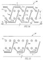
- FIGS 13-15 display a third alternative embodiment of a circuit substrate to which receptacle 101 mounts.
- the substrate comprises a multi-layer board (MLB) 501.
- MLB 501 closely resembles MLB 401, save the sixth and seventh layers.
- a sixth layer 545 and an adjacent seventh layer 547 have conductors thereon.
- sixth and seventh layers 445, 447 preferably create a compensating cross-talk that offsets unwanted cross-talk between twice removed conductors.
- Figures 14 and 15 demonstrate the particular arrangement of conductors on the sixth and seventh layers 445, 447.
- sixth layer 545 displays conductor C 16,b from sixteenth differential pair DP 16 extending forwardly to a position adjacent conductor C 13,a from thirteenth differential pair DP 13 .
- Conductors C 16,b , C 13,a extend adjacently at an area A to create the necessary compensating cross-talk between twice removed conductors.
- the other conductor C 16,a from sixteenth differential pair DP 16 extends forwardly to a position adjacent conductor C 19,b from nineteenth differential pair DP 19 .
- Conductors C 16,a , C 19,b extend adjacently at an area A to create the necessary compensating cross-talk between twice removed conductors.
- conductors from an adjacent differential pair extend rearwardly to overlap with their corresponding twice removed conductors.
- conductor C 17,b from seventeenth differential pair DP 17 extends rearwardly to a position adjacent conductor C 14,a from fourteenth differential pair DP 14 .
- the other conductor C 17,a from seventeenth differential pair DP 17 extends rearwardly to a position adjacent conductor C 20,b from twentieth differential pair DP 20 .
- seventh layer 547 displays conductor C 15,b from fifteenth differential pair DP 15 extending forwardly to a position adjacent conductor C 12,a from twelfth differential pair DP 12 .
- An overlap O between conductors C 15,b , C 12,a extend adjacently at area A to create the necessary compensating cross-talk between twice removed conductors.
- the other conductor C 15,a from fifteenth differential pair DP 15 extends forwardly to a position adjacent conductor C 18,b from eighteenth differential pair DP 18 .
- Conductors C 15,a , C 18,b c extend adjacently at area A to create the necessary compensating cross-talk between twice removed conductors.
- the conductors on seventh layer 547 extend further from through holes 511 than the conductors on sixth layer 545. This prevents any adverse cross-talk between the conductors on the adjacent sixth and seventh layers 545, 547.
- the conductors on seventh layer 547 could extend to a position medial the rows of through holes 511 (not shown). This location would also prevent adverse cross-talk between conductors on the adjacent sixth and seventh layers 545, 547.
- the conductors are stubs, not electrically connecting through holes 411.
- the geometry of the conductors and the spacing between the sixth and seventh layers 545, 547 and between adjacent conductors determines the amount of compensating cross-talk.
- Each conductor on sixth and seventh layers 545, 547 preferably has a generally uniform width. The width of the conductors and a gap G between the conductors is selected to form the desired amount of compensating cross-talk.
- the width suitable to form the desired amount of compensating cross-talk depends on the length of an overlap A. Generally speaking, for smaller gaps G, the smaller the length of overlap A can be. For greater lengths of gaps G, the greater the length of overlap A can be.
Landscapes
- Physics & Mathematics (AREA)
- Electromagnetism (AREA)
- Engineering & Computer Science (AREA)
- Microelectronics & Electronic Packaging (AREA)
- Details Of Connecting Devices For Male And Female Coupling (AREA)
- Coupling Device And Connection With Printed Circuit (AREA)
- Production Of Multi-Layered Print Wiring Board (AREA)
- Structure Of Printed Boards (AREA)
Applications Claiming Priority (2)
| Application Number | Priority Date | Filing Date | Title |
|---|---|---|---|
| US09/353,184 US6250968B1 (en) | 1999-07-14 | 1999-07-14 | Electrical connector system with cross-talk compensation |
| US353184 | 1999-07-14 |
Publications (2)
| Publication Number | Publication Date |
|---|---|
| EP1069655A2 true EP1069655A2 (fr) | 2001-01-17 |
| EP1069655A3 EP1069655A3 (fr) | 2002-04-17 |
Family
ID=23388094
Family Applications (1)
| Application Number | Title | Priority Date | Filing Date |
|---|---|---|---|
| EP00114190A Withdrawn EP1069655A3 (fr) | 1999-07-14 | 2000-07-13 | Connecteur électrique à diaphonie réduite |
Country Status (5)
| Country | Link |
|---|---|
| US (1) | US6250968B1 (fr) |
| EP (1) | EP1069655A3 (fr) |
| JP (1) | JP2001057259A (fr) |
| KR (1) | KR100778215B1 (fr) |
| CA (1) | CA2313679C (fr) |
Cited By (6)
| Publication number | Priority date | Publication date | Assignee | Title |
|---|---|---|---|---|
| US7549897B2 (en) | 2006-08-02 | 2009-06-23 | Tyco Electronics Corporation | Electrical connector having improved terminal configuration |
| US7591655B2 (en) | 2006-08-02 | 2009-09-22 | Tyco Electronics Corporation | Electrical connector having improved electrical characteristics |
| US7670196B2 (en) | 2006-08-02 | 2010-03-02 | Tyco Electronics Corporation | Electrical terminal having tactile feedback tip and electrical connector for use therewith |
| US7753742B2 (en) | 2006-08-02 | 2010-07-13 | Tyco Electronics Corporation | Electrical terminal having improved insertion characteristics and electrical connector for use therewith |
| EP2209172A1 (fr) * | 2009-01-15 | 2010-07-21 | 3M Innovative Properties Company | Connecteur de télécommunications doté d'une carte à circuit imprimé multicouche |
| US8142236B2 (en) | 2006-08-02 | 2012-03-27 | Tyco Electronics Corporation | Electrical connector having improved density and routing characteristics and related methods |
Families Citing this family (25)
| Publication number | Priority date | Publication date | Assignee | Title |
|---|---|---|---|---|
| US6614325B1 (en) * | 2000-08-31 | 2003-09-02 | Northrop Grumman Corporation | RF/IF signal distribution network utilizing broadside coupled stripline |
| US6511344B2 (en) * | 2001-07-02 | 2003-01-28 | Fci Americas Technology, Inc. | Double-deck electrical connector with cross-talk compensation |
| US20030150643A1 (en) * | 2002-02-13 | 2003-08-14 | Eric Juntwait | Layout for noise reduction on a printed circuit board and connectors using it |
| BR0315712A (pt) * | 2002-11-20 | 2005-09-06 | Siemon Co | Placa de circuito impresso que fornece compensação de linha cruzada e conector de telecomunicação |
| US7265300B2 (en) | 2003-03-21 | 2007-09-04 | Commscope Solutions Properties, Llc | Next high frequency improvement using hybrid substrates of two materials with different dielectric constant frequency slopes |
| US7153168B2 (en) * | 2004-04-06 | 2006-12-26 | Panduit Corp. | Electrical connector with improved crosstalk compensation |
| US7179115B2 (en) * | 2004-04-26 | 2007-02-20 | Commscope Solutions Properties, Llc | Alien next compensation for adjacently placed connectors |
| US7190594B2 (en) * | 2004-05-14 | 2007-03-13 | Commscope Solutions Properties, Llc | Next high frequency improvement by using frequency dependent effective capacitance |
| US7980900B2 (en) * | 2004-05-14 | 2011-07-19 | Commscope, Inc. Of North Carolina | Next high frequency improvement by using frequency dependent effective capacitance |
| US7571408B1 (en) * | 2005-03-09 | 2009-08-04 | Cadence Design Systems, Inc. | Methods and apparatus for diagonal route shielding |
| JP4816007B2 (ja) * | 2005-10-31 | 2011-11-16 | ソニー株式会社 | フレキシブル基板用コネクタ、基板接続構造、光送受信モジュール及び光送受信装置 |
| JP2009527079A (ja) * | 2006-02-13 | 2009-07-23 | パンデュイット・コーポレーション | 漏話補償機能付きコネクタ |
| US7488206B2 (en) * | 2006-02-14 | 2009-02-10 | Panduit Corp. | Method and apparatus for patch panel patch cord documentation and revision |
| US20070275607A1 (en) * | 2006-05-04 | 2007-11-29 | Kwark Young H | Compensation for far end crosstalk in data buses |
| US7874878B2 (en) | 2007-03-20 | 2011-01-25 | Panduit Corp. | Plug/jack system having PCB with lattice network |
| US20090283318A1 (en) * | 2008-05-13 | 2009-11-19 | Honeywell International Inc. | Integrated EMI Shield Termination and Cable Support Apparatus |
| US9627816B2 (en) | 2012-02-13 | 2017-04-18 | Sentinel Connector System Inc. | High speed grounded communication jack |
| US8858266B2 (en) * | 2012-02-13 | 2014-10-14 | Sentinel Connector Systems, Inc. | High speed communication jack |
| US9653847B2 (en) | 2013-01-11 | 2017-05-16 | Sentinel Connector System, Inc. | High speed communication jack |
| US9337592B2 (en) | 2012-02-13 | 2016-05-10 | Sentinel Connector Systems, Inc. | High speed communication jack |
| US9545003B2 (en) * | 2012-12-28 | 2017-01-10 | Fci Americas Technology Llc | Connector footprints in printed circuit board (PCB) |
| BR112017006086A2 (pt) * | 2014-10-01 | 2017-12-19 | Sentinel Connector Systems Inc | tomada para comunicação em alta velocidade |
| US9912083B2 (en) | 2015-07-21 | 2018-03-06 | Sentinel Connector Systems, Inc. | High speed plug |
| CA3021559A1 (fr) | 2016-05-04 | 2017-11-09 | Sentinel Connector Systems, Inc. | Fiche industrielle a grand conducteur |
| CN109193204B (zh) * | 2018-08-24 | 2023-09-26 | 四川华丰科技股份有限公司 | 非等宽交错式走线电连接器及电子设备 |
Citations (4)
| Publication number | Priority date | Publication date | Assignee | Title |
|---|---|---|---|---|
| EP0692841A1 (fr) * | 1994-07-15 | 1996-01-17 | Connector Systems Technology N.V. | Assemblage d'un connecteur blindé et un circuit imprimé à l'aide de trous métallisés |
| GB2314466A (en) * | 1996-06-21 | 1997-12-24 | Lucent Technologies Inc | Capacitor array for reducing cross-talk in connectors |
| EP0854664A1 (fr) * | 1997-01-16 | 1998-07-22 | Lucent Technologies Inc. | Planche de cablage imprimé avec compensation de diaphonique |
| EP1049217A1 (fr) * | 1999-04-27 | 2000-11-02 | Lucent Technologies Inc. | Connecteur ayant compensation de diaphonie interne |
Family Cites Families (9)
| Publication number | Priority date | Publication date | Assignee | Title |
|---|---|---|---|---|
| US5287066A (en) | 1992-05-15 | 1994-02-15 | The Grass Valley Group | Crosstalk reduction circuit for crosspoint matrix |
| GB2284511B (en) | 1992-08-24 | 1996-12-04 | British Telecomm | Apparatus for crosstalk cancellation in data connectors |
| US6065994A (en) | 1996-06-21 | 2000-05-23 | Lucent Technologies Inc. | Low-crosstalk electrical connector grouping like conductors together |
| US5700167A (en) | 1996-09-06 | 1997-12-23 | Lucent Technologies | Connector cross-talk compensation |
| US5952607A (en) | 1997-01-31 | 1999-09-14 | Lucent Technologies Inc. | Local area network cabling arrangement |
| US5797764A (en) | 1997-02-12 | 1998-08-25 | Homaco, Inc. | Low return loss and low crosstalk telecommunications electric circuit |
| US5997358A (en) * | 1997-09-02 | 1999-12-07 | Lucent Technologies Inc. | Electrical connector having time-delayed signal compensation |
| KR19990001111A (ko) * | 1997-06-12 | 1999-01-15 | 윤종용 | 크로스토크 감소 기능을 갖는 pga 회로 |
| US5967801A (en) | 1997-11-26 | 1999-10-19 | The Whitaker Corporation | Modular plug having compensating insert |
-
1999
- 1999-07-14 US US09/353,184 patent/US6250968B1/en not_active Expired - Lifetime
-
2000
- 2000-07-04 JP JP2000202664A patent/JP2001057259A/ja active Pending
- 2000-07-10 CA CA002313679A patent/CA2313679C/fr not_active Expired - Fee Related
- 2000-07-13 EP EP00114190A patent/EP1069655A3/fr not_active Withdrawn
- 2000-07-13 KR KR1020000040105A patent/KR100778215B1/ko not_active Expired - Fee Related
Patent Citations (4)
| Publication number | Priority date | Publication date | Assignee | Title |
|---|---|---|---|---|
| EP0692841A1 (fr) * | 1994-07-15 | 1996-01-17 | Connector Systems Technology N.V. | Assemblage d'un connecteur blindé et un circuit imprimé à l'aide de trous métallisés |
| GB2314466A (en) * | 1996-06-21 | 1997-12-24 | Lucent Technologies Inc | Capacitor array for reducing cross-talk in connectors |
| EP0854664A1 (fr) * | 1997-01-16 | 1998-07-22 | Lucent Technologies Inc. | Planche de cablage imprimé avec compensation de diaphonique |
| EP1049217A1 (fr) * | 1999-04-27 | 2000-11-02 | Lucent Technologies Inc. | Connecteur ayant compensation de diaphonie interne |
Cited By (10)
| Publication number | Priority date | Publication date | Assignee | Title |
|---|---|---|---|---|
| US7549897B2 (en) | 2006-08-02 | 2009-06-23 | Tyco Electronics Corporation | Electrical connector having improved terminal configuration |
| US7591655B2 (en) | 2006-08-02 | 2009-09-22 | Tyco Electronics Corporation | Electrical connector having improved electrical characteristics |
| US7670196B2 (en) | 2006-08-02 | 2010-03-02 | Tyco Electronics Corporation | Electrical terminal having tactile feedback tip and electrical connector for use therewith |
| US7753742B2 (en) | 2006-08-02 | 2010-07-13 | Tyco Electronics Corporation | Electrical terminal having improved insertion characteristics and electrical connector for use therewith |
| US7789716B2 (en) | 2006-08-02 | 2010-09-07 | Tyco Electronics Corporation | Electrical connector having improved terminal configuration |
| US8142236B2 (en) | 2006-08-02 | 2012-03-27 | Tyco Electronics Corporation | Electrical connector having improved density and routing characteristics and related methods |
| EP2209172A1 (fr) * | 2009-01-15 | 2010-07-21 | 3M Innovative Properties Company | Connecteur de télécommunications doté d'une carte à circuit imprimé multicouche |
| WO2010083150A1 (fr) * | 2009-01-15 | 2010-07-22 | 3M Innovative Properties Company | Prise de télécommunications à carte imprimée multicouche |
| CN102349201A (zh) * | 2009-01-15 | 2012-02-08 | 3M创新有限公司 | 具有多层pcb的电信插座 |
| US8282424B2 (en) | 2009-01-15 | 2012-10-09 | 3M Innovative Properties Company | Telecommunications jack with a multilayer PCB |
Also Published As
| Publication number | Publication date |
|---|---|
| EP1069655A3 (fr) | 2002-04-17 |
| US6250968B1 (en) | 2001-06-26 |
| JP2001057259A (ja) | 2001-02-27 |
| KR100778215B1 (ko) | 2007-11-20 |
| KR20010015315A (en) | 2001-02-26 |
| CA2313679C (fr) | 2008-01-29 |
| CA2313679A1 (fr) | 2001-01-14 |
Similar Documents
| Publication | Publication Date | Title |
|---|---|---|
| US6250968B1 (en) | Electrical connector system with cross-talk compensation | |
| US7204722B2 (en) | Communications jack with compensation for differential to differential and differential to common mode crosstalk | |
| US6464541B1 (en) | Simultaneous near-end and far-end crosstalk compensation in a communication connector | |
| US7168993B2 (en) | Communications connector with floating wiring board for imparting crosstalk compensation between conductors | |
| US7320624B2 (en) | Communications jacks with compensation for differential to differential and differential to common mode crosstalk | |
| EP1096620B1 (fr) | Compensation capacitive de la diaphonie pour un connecteur de télécommunication | |
| US7682203B1 (en) | Communications jacks having contact wire configurations that provide crosstalk compensation | |
| US7186149B2 (en) | Communications connector for imparting enhanced crosstalk compensation between conductors | |
| EP0854664B1 (fr) | Dispositif pour la compensation de la diaphonie dans un connecteur | |
| US7364470B2 (en) | Communications connectors with signal current splitting | |
| US6520807B2 (en) | Electrical connector system with low cross-talk | |
| US7314393B2 (en) | Communications connectors with floating wiring board for imparting crosstalk compensation between conductors | |
| EP1160935B1 (fr) | Connecteur de communication avec compensation de diaphonie | |
| EP3139453A1 (fr) | Connecteur rj45 comprenant une circuiterie d'amélioration d'affaiblissement de réflexion | |
| US7186148B2 (en) | Communications connector for imparting crosstalk compensation between conductors | |
| US6511344B2 (en) | Double-deck electrical connector with cross-talk compensation | |
| AU2009210388B2 (en) | Communications jack with compensation for differential to differential and differential to common mode crosstalk | |
| EP1820285B1 (fr) | Connecteur de communication comportant une carte de connexion flottante permettant de compenser la diaphonie entre de cables |
Legal Events
| Date | Code | Title | Description |
|---|---|---|---|
| PUAI | Public reference made under article 153(3) epc to a published international application that has entered the european phase |
Free format text: ORIGINAL CODE: 0009012 |
|
| AK | Designated contracting states |
Kind code of ref document: A2 Designated state(s): AT BE CH CY DE DK ES FI FR GB GR IE IT LI LU MC NL PT SE |
|
| AX | Request for extension of the european patent |
Free format text: AL;LT;LV;MK;RO;SI |
|
| PUAL | Search report despatched |
Free format text: ORIGINAL CODE: 0009013 |
|
| AK | Designated contracting states |
Kind code of ref document: A3 Designated state(s): AT BE CH CY DE DK ES FI FR GB GR IE IT LI LU MC NL PT SE |
|
| AX | Request for extension of the european patent |
Free format text: AL;LT;LV;MK;RO;SI |
|
| RIC1 | Information provided on ipc code assigned before grant |
Free format text: 7H 01R 24/00 A, 7H 05K 1/02 B |
|
| 17P | Request for examination filed |
Effective date: 20021004 |
|
| AKX | Designation fees paid |
Free format text: AT BE CH CY DE DK ES FI FR GB GR IE IT LI LU MC NL PT SE |
|
| 17Q | First examination report despatched |
Effective date: 20070411 |
|
| STAA | Information on the status of an ep patent application or granted ep patent |
Free format text: STATUS: THE APPLICATION IS DEEMED TO BE WITHDRAWN |
|
| 18D | Application deemed to be withdrawn |
Effective date: 20091006 |