EP1069608A1 - Method of wire bonding, semiconductor device, circuit board, electronic device and wire bonder - Google Patents
Method of wire bonding, semiconductor device, circuit board, electronic device and wire bonder Download PDFInfo
- Publication number
- EP1069608A1 EP1069608A1 EP00900809A EP00900809A EP1069608A1 EP 1069608 A1 EP1069608 A1 EP 1069608A1 EP 00900809 A EP00900809 A EP 00900809A EP 00900809 A EP00900809 A EP 00900809A EP 1069608 A1 EP1069608 A1 EP 1069608A1
- Authority
- EP
- European Patent Office
- Prior art keywords
- wire
- electrodes
- imaginary
- straight line
- leads
- Prior art date
- Legal status (The legal status is an assumption and is not a legal conclusion. Google has not performed a legal analysis and makes no representation as to the accuracy of the status listed.)
- Granted
Links
Images

Classifications
-
- H—ELECTRICITY
- H10—SEMICONDUCTOR DEVICES; ELECTRIC SOLID-STATE DEVICES NOT OTHERWISE PROVIDED FOR
- H10W—GENERIC PACKAGES, INTERCONNECTIONS, CONNECTORS OR OTHER CONSTRUCTIONAL DETAILS OF DEVICES COVERED BY CLASS H10
- H10W70/00—Package substrates; Interposers; Redistribution layers [RDL]
- H10W70/40—Leadframes
- H10W70/464—Additional interconnections in combination with leadframes
- H10W70/465—Bumps or wires
-
- H—ELECTRICITY
- H10—SEMICONDUCTOR DEVICES; ELECTRIC SOLID-STATE DEVICES NOT OTHERWISE PROVIDED FOR
- H10W—GENERIC PACKAGES, INTERCONNECTIONS, CONNECTORS OR OTHER CONSTRUCTIONAL DETAILS OF DEVICES COVERED BY CLASS H10
- H10W72/00—Interconnections or connectors in packages
- H10W72/071—Connecting or disconnecting
- H10W72/0711—Apparatus therefor
- H10W72/07141—Means for applying energy, e.g. ovens or lasers
-
- H—ELECTRICITY
- H10—SEMICONDUCTOR DEVICES; ELECTRIC SOLID-STATE DEVICES NOT OTHERWISE PROVIDED FOR
- H10W—GENERIC PACKAGES, INTERCONNECTIONS, CONNECTORS OR OTHER CONSTRUCTIONAL DETAILS OF DEVICES COVERED BY CLASS H10
- H10W72/00—Interconnections or connectors in packages
- H10W72/071—Connecting or disconnecting
- H10W72/075—Connecting or disconnecting of bond wires
- H10W72/07521—Aligning
-
- H—ELECTRICITY
- H10—SEMICONDUCTOR DEVICES; ELECTRIC SOLID-STATE DEVICES NOT OTHERWISE PROVIDED FOR
- H10W—GENERIC PACKAGES, INTERCONNECTIONS, CONNECTORS OR OTHER CONSTRUCTIONAL DETAILS OF DEVICES COVERED BY CLASS H10
- H10W72/00—Interconnections or connectors in packages
- H10W72/071—Connecting or disconnecting
- H10W72/075—Connecting or disconnecting of bond wires
- H10W72/07541—Controlling the environment, e.g. atmosphere composition or temperature
- H10W72/07553—Controlling the environment, e.g. atmosphere composition or temperature changes in shapes
-
- H—ELECTRICITY
- H10—SEMICONDUCTOR DEVICES; ELECTRIC SOLID-STATE DEVICES NOT OTHERWISE PROVIDED FOR
- H10W—GENERIC PACKAGES, INTERCONNECTIONS, CONNECTORS OR OTHER CONSTRUCTIONAL DETAILS OF DEVICES COVERED BY CLASS H10
- H10W72/00—Interconnections or connectors in packages
- H10W72/50—Bond wires
- H10W72/531—Shapes of wire connectors
- H10W72/5363—Shapes of wire connectors the connected ends being wedge-shaped
-
- H—ELECTRICITY
- H10—SEMICONDUCTOR DEVICES; ELECTRIC SOLID-STATE DEVICES NOT OTHERWISE PROVIDED FOR
- H10W—GENERIC PACKAGES, INTERCONNECTIONS, CONNECTORS OR OTHER CONSTRUCTIONAL DETAILS OF DEVICES COVERED BY CLASS H10
- H10W72/00—Interconnections or connectors in packages
- H10W72/50—Bond wires
- H10W72/541—Dispositions of bond wires
- H10W72/5445—Dispositions of bond wires being orthogonal to a side surface of the chip, e.g. parallel arrangements
-
- H—ELECTRICITY
- H10—SEMICONDUCTOR DEVICES; ELECTRIC SOLID-STATE DEVICES NOT OTHERWISE PROVIDED FOR
- H10W—GENERIC PACKAGES, INTERCONNECTIONS, CONNECTORS OR OTHER CONSTRUCTIONAL DETAILS OF DEVICES COVERED BY CLASS H10
- H10W72/00—Interconnections or connectors in packages
- H10W72/50—Bond wires
- H10W72/541—Dispositions of bond wires
- H10W72/5449—Dispositions of bond wires not being orthogonal to a side surface of the chip, e.g. fan-out arrangements
-
- H—ELECTRICITY
- H10—SEMICONDUCTOR DEVICES; ELECTRIC SOLID-STATE DEVICES NOT OTHERWISE PROVIDED FOR
- H10W—GENERIC PACKAGES, INTERCONNECTIONS, CONNECTORS OR OTHER CONSTRUCTIONAL DETAILS OF DEVICES COVERED BY CLASS H10
- H10W72/00—Interconnections or connectors in packages
- H10W72/851—Dispositions of multiple connectors or interconnections
- H10W72/874—On different surfaces
- H10W72/884—Die-attach connectors and bond wires
-
- H—ELECTRICITY
- H10—SEMICONDUCTOR DEVICES; ELECTRIC SOLID-STATE DEVICES NOT OTHERWISE PROVIDED FOR
- H10W—GENERIC PACKAGES, INTERCONNECTIONS, CONNECTORS OR OTHER CONSTRUCTIONAL DETAILS OF DEVICES COVERED BY CLASS H10
- H10W72/00—Interconnections or connectors in packages
- H10W72/90—Bond pads, in general
- H10W72/931—Shapes of bond pads
- H10W72/932—Plan-view shape, i.e. in top view
-
- H—ELECTRICITY
- H10—SEMICONDUCTOR DEVICES; ELECTRIC SOLID-STATE DEVICES NOT OTHERWISE PROVIDED FOR
- H10W—GENERIC PACKAGES, INTERCONNECTIONS, CONNECTORS OR OTHER CONSTRUCTIONAL DETAILS OF DEVICES COVERED BY CLASS H10
- H10W72/00—Interconnections or connectors in packages
- H10W72/90—Bond pads, in general
- H10W72/951—Materials of bond pads
- H10W72/952—Materials of bond pads comprising metals or metalloids, e.g. PbSn, Ag or Cu
-
- H—ELECTRICITY
- H10—SEMICONDUCTOR DEVICES; ELECTRIC SOLID-STATE DEVICES NOT OTHERWISE PROVIDED FOR
- H10W—GENERIC PACKAGES, INTERCONNECTIONS, CONNECTORS OR OTHER CONSTRUCTIONAL DETAILS OF DEVICES COVERED BY CLASS H10
- H10W74/00—Encapsulations, e.g. protective coatings
-
- H—ELECTRICITY
- H10—SEMICONDUCTOR DEVICES; ELECTRIC SOLID-STATE DEVICES NOT OTHERWISE PROVIDED FOR
- H10W—GENERIC PACKAGES, INTERCONNECTIONS, CONNECTORS OR OTHER CONSTRUCTIONAL DETAILS OF DEVICES COVERED BY CLASS H10
- H10W90/00—Package configurations
- H10W90/701—Package configurations characterised by the relative positions of pads or connectors relative to package parts
- H10W90/731—Package configurations characterised by the relative positions of pads or connectors relative to package parts of die-attach connectors
- H10W90/734—Package configurations characterised by the relative positions of pads or connectors relative to package parts of die-attach connectors between a chip and a stacked insulating package substrate, interposer or RDL
-
- H—ELECTRICITY
- H10—SEMICONDUCTOR DEVICES; ELECTRIC SOLID-STATE DEVICES NOT OTHERWISE PROVIDED FOR
- H10W—GENERIC PACKAGES, INTERCONNECTIONS, CONNECTORS OR OTHER CONSTRUCTIONAL DETAILS OF DEVICES COVERED BY CLASS H10
- H10W90/00—Package configurations
- H10W90/701—Package configurations characterised by the relative positions of pads or connectors relative to package parts
- H10W90/751—Package configurations characterised by the relative positions of pads or connectors relative to package parts of bond wires
- H10W90/754—Package configurations characterised by the relative positions of pads or connectors relative to package parts of bond wires between a chip and a stacked insulating package substrate, interposer or RDL
Definitions
- the present invention relates to a wire bonding method, a semiconductor device, a circuit board, an electronic instrument and a wire bonding device.
- wire bonding technology is applied in order to electrically connect the electrodes of a semiconductor chip to leads.
- the pin-counts of semiconductor devices has been rising, but with conventional wire bonding technology, there are limits to wire lead-out, and therefore it has only been possible to support this by means of the form or layout of the electrodes of the semiconductor chip, or the form or construction of the leads.
- the present invention solves this problem, and has as its objective the provision of a wire bonding method which allows a free lead-out of the wires, a semiconductor device manufactured by this method, a circuit board and electronic instrument provided with the semiconductor device, and a wire bonding device using this method.
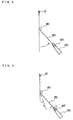
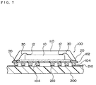
- Fig. 1 shows an embodiment of the wire bonding method to which the present invention is applied. As shown in Fig. 1, a semiconductor chip 10 on which an integrated circuit is formed, and a plurality of leads 20 are provided.
- each of the electrodes 12 is aligned in a single row on a first imaginary straight line L1, with a substantially uniform center-to-center spacing (pitch).
- the form of each of the electrodes 12 may be rectangular, such that the edges in the direction of alignment of the row (parallel to the imaginary straight line L1) are shorter than the edges perpendicular thereto.
- the number of electrodes 12 is increased, so the center-to-center spacing of the electrodes 12 is reduced, and therefore the length of the edge in the direction of alignment is also reduced, but the length of the edge in the direction perpendicular thereto can be designed with relative freedom.
- the electrodes 12 can be made large, and a large bonding area can be provided.
- the electrodes 12 may be aligned along two sides which are parallel to each other, or may equally be aligned along the four sides.
- the electrodes 12 may be disposed in a central portion of the semiconductor chip 10 or on the periphery thereof. A passivation film is commonly formed on the active surface, avoiding the electrodes 12.
- the leads 20 may be the inner leads of a lead frame, or may be interconnects formed on a substrate. When the leads 20 form part of a semiconductor device, they are electrically connected to the external terminals of the semiconductor device.
- the leads 20 are aligned in an imaginary plane P.
- the imaginary plane P is preferably parallel to the plane in which the electrodes 12 of the semiconductor chip 10 are formed, and may be the same plane.
- the leads 20 are wider than the electrodes 12, and the center-to-center spacing (pitch) is also wider than the center-to-center spacing of the electrodes 12.
- Each of the leads 20 is commonly electrically connected to one of the electrodes 12, but may equally be electrically connected to a plurality of the electrodes 12, of a plurality of leads 20 may be electrically connected to a single electrode 12.
- the plurality of leads 20 could be aligned parallel to the plurality of electrodes 12, but in this case, leads 20 closer to the ends of the row are farther from the electrodes 12. That is to say, the distance from the electrodes 12 to the leads 20 is different in the central portion and the periphery of the semiconductor chip 10, and in particular, the distance from the end electrodes 12 to the corresponding leads 20 is longer. Therefore, as shown in Fig. 1, the ends of the plurality of leads 20 are disposed on an imaginary line L which is different from the third imaginary straight line L3 which is parallel to the first imaginary straight line L1.
- the imaginary line L may be a straight line or it may be a curved line.
- the imaginary line L is preferably closer to the electrodes 12 than the third imaginary straight line L3.
- the leads 20 close to the end of the row are brought closer to the electrodes 12, and therefore the distance between the leads 20 and the electrodes 12 can be made less.
- the leads 20 and electrodes 12 are connected one-to-one, the leads 20 may be disposed so that the lengths of respective wires 30 are substantially equal.
- the plurality of leads 20 is disposed on the periphery of the semiconductor chip 10, and wire bonding is carried out.
- wire bonding For example, ball bonding or wedge bonding is carried out.
- wires 30 are bonded to one of the electrodes 12 and leads 20 at first.
- the first wire 30 is preferably bonded to the electrode 12 or lead 20 closest to the imaginary vertical line LV passing through the mid-point M between a pair of electrodes 12 positioned at both ends of the row, as viewed from a direction perpendicular to the imaginary plane P (or perpendicular to the sheet surface of Fig. 1).
- the wires 30 are commonly bonded to the corresponding leads 20 after being bonded to the electrodes 12.
- the wires 30 are further drawn out.
- the wires 30 may describe a loop shape in three dimensions. If the wires 30 have been bonded to the electrodes 12 in the second step, it is preferable that the wires 30 are drawn out parallel to the imaginary vertical line LV, as viewed from a direction perpendicular to the imaginary plane P (or perpendicular to the sheet surface of Fig. 1). By doing this, the plurality of wires 30 can be drawn out parallel, at substantially the same spacing as the electrodes 12. When wedge bonding is applied, and the electrodes 12 form a rectangle with sides parallel to the first imaginary straight line L1 and sides perpendicular thereto, the wires 30 can be bonded to the electrodes 12 without becoming diagonal.
- the wires 30 are bent toward the other of the electrodes 12 and leads 20.
- the wires 30 can be contacted against a pin (or pole) 40, whereby the wires 30 are bent. If the first wire 30 is bonded to the electrode 12 or lead 20 closest to the imaginary vertical line LV passing through the mid-point M, and the wire 30 is then bent in a direction away from the imaginary vertical line LV, when the pin 40 is moved to the position of the next wire 30, the previously laid down wire 30 does not form an obstruction.
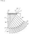
- Figs. 2 and 3 show examples of the bending of the wires 30.
- the wire 30 of a required length may be drawn out in a straight line from the electrode 12 to be bent by means of the pin 40 after drawing out.
- the "required length” is the length required to form an electrical connection between the electrodes 12 and the leads 20.
- the wire 30 may be drawn out as far as the bending position in a straight line, and then as this wire 30 is bent, it may be further drawn out.
- the wire 30 is bonded to the other of the electrode 12 or lead 20. With this step, the wire bonding of a single wire 30 is completed.
- the above first to fourth steps are again used, to carry out wire bonding of all of the electrodes 12 and leads 20.
- the first wire 30 has been bonded to the electrode 12 and lead 20 closest to the imaginary vertical line LV, then the next wire 30 is bonded to the electrode 12 and lead 20 second closest to the imaginary vertical line LV.
- the bent portions of the wires 30 are preferably aligned on a single straight line. If this is done, the spacing of the bent portions of the wires 30 can be made substantially uniform. Moreover, if the bent portions of the wires 30 are aligned on a straight line intersecting the first imaginary straight line L1 and the imaginary vertical line LV, then the spacing can be increased.
- the wires 30 are preferably bent on a second imaginary straight line L2 which has an inclination similar to this curved line.
- the second imaginary straight line L2 intersects the first imaginary straight line L1 at a point of intersection C.
- the distance from the electrode 12 closest to the point of intersection C to the second imaginary straight line L2 is less than the distance from the second imaginary straight line L2 to the mid-point M. If this is made so, the spacing of the wires 30 can be increased on the side of the leads 20 from the second imaginary straight line L2.
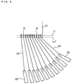
- the point of intersection C' of the second imaginary straight line L2' and the first imaginary straight line L1 it is preferable for the point of intersection C' of the second imaginary straight line L2' and the first imaginary straight line L1 to be closest to the electrodes 12, and the point of intersection C'' of the second imaginary straight line L2' and the imaginary vertical line LV to be furthest from the electrodes 12. If the wires 30 are bent on this second imaginary straight line L2', the maximum spacing between the wires 30 can be obtained.
- the wires 30 may be bent on a second imaginary straight line L2'' parallel to the first imaginary straight line L1.
- the second imaginary straight line L2'' is preferably made close to the electrodes 12.
- the second imaginary straight line L2'' is disposed close to the periphery of the semiconductor chip 10, but it may equally be disposed on the periphery of the electrodes 12. It may be disposed between the periphery of the semiconductor chip 10 and the periphery of the electrodes 12, for example at the mid-point.
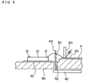
- Fig. 6 shows an embodiment of a wire bonding device to which the present invention is applied.
- the wire bonding device shown in Fig. 6 comprises a pin (pole) 40, a table 50 and a bonding tool 60.
- the table 50 is adapted to have the semiconductor chip 10 and plurality of leads 20 mounted thereon. It should be noted that when a lead frame is used, the semiconductor chip 10 is mounted on a die pad 70, and the semiconductor chip 10 is mounted on the table 50 with the die pad 70 interposed.
- the leads 20 are aligned in the imaginary plane P.
- the imaginary plane P is preferably parallel to the plane in which the electrodes 12 of the semiconductor chip 10 are formed, and may be the same plane, or may be a different plane. It should be noted that the leads 20 are wider than the electrodes 12, and the center-to-center spacing (pitch) is also more than the center-to-center spacing of the electrodes 12. For the arrangement and form of the leads 20, the description of the wire bonding method can be applied.
- the bonding tool 60 bonds wires 30 to the electrodes 12 and leads 20, and includes a bonding head, wire clamp, and so on. In order to bend the wires 30, the bonding tool 60 moves in a non-straight line as viewed from a direction perpendicular to the imaginary plane P (or perpendicular to the sheet surface of Fig. 1).
- the bonding tool 60 When bending the wires 30, the bonding tool 60 may be moved in such a way as to apply the method described in Figs. 2 and 3.
- the bonding tool 60 may be moved in a straight line from the electrodes 12 until the required length for the wires 30 is achieved, then the bonding tool 60 moved to describe an arc about the pin 40, in order to bend the wires 30.
- the "required length" is the length required to form an electrical connection between the electrodes 12 and the leads 20.
- the bonding tool 60 may be moved in a straight line as far as the bending position, then the bonding tool 60 moved to rotate about the pin 40 while receding from the pin 40, so as to bend the wires 30.
- the pin 40 as in the wire bonding method described above, is used to bend the wires 30.
- the pin 40 as shown in Fig. 1, is moved after bonding one of the wires 30, to bond the next of the wires 30.
- the pin 40 is provided on an arm 42, and can be moved by this arm 42.
- the arm 42 may be provided on the opposite surface of the table 50 from that on which the semiconductor chip 10 is mounted. In this case, a slot 52 may be formed in the table 50 along the path of movement of the pin 40.
- the arm 42 may be provided to support the pin 40 on the side on which the semiconductor chip 10 is disposed.
- a mechanism may be provided such that the lead frame or the like is transported and moved to a bonding stage, then when clamped and fixed, the pin 40 can be removed in their axial direction, or coupled to a clamp such that the pin 40 is inserted and retracted.
- This embodiment of the wire bonding device operates to implement the above-described wire bonding method.
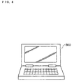
- Fig. 7 shows a circuit board on which is mounted an embodiment of a semiconductor device to which the present invention is applied.
- a semiconductor device to which CSP is applied.
- QFP Quad Flat Package
- BGA Bit Grid Array
- CSP Chip Scale/Size Package
- a semiconductor device to which CSP is applied is shown in Fig. 7.
- a semiconductor device 100 comprises a semiconductor chip 10 having a plurality of electrodes 12, a plurality of leads 20, a plurality of wires 30, a resin 110 sealing at least a bonding portion, a substrate 102, and a plurality of external terminals 104 such as solder balls.
- the wires 30 are bent to electrically connect the electrodes 12 and leads 20, as shown in Fig. 1. In more detail, the description of the above wire bonding method is applied. According to the semiconductor device 100, the spacing of the wires 30 is large, and therefore contact between adjacent wires 30 can be prevented.
- a circuit board 200 For a circuit board 200 is generally used an organic substrate such as for example a glass epoxy substrate. On the circuit board 200 a desired circuit is formed from an interconnect pattern 210 of for example copper, and this interconnect pattern 210 is mechanically connected to the external terminals 104 of the semiconductor device 100, whereby electrical connections are established.
- Fig. 8 shows a notebook personal computer.
- semiconductor chip of the present invention may be replaced by "electronic element,” and an electronic element (whether an active element or a passive element) can be used in the same way as a semiconductor chip.
- electronic components manufactured using such an electronic element may be cited, for example, resistors, capacitors, coils, oscillators, filters, temperature sensors, thermistors, varistors, variable resistors, and fuses.
Landscapes
- Wire Bonding (AREA)
Abstract
Description
wherein the bonding tool moves between a pair formed by one of the electrodes and one of the leads, along a non-straight line as viewed from a direction perpendicular to the imaginary plane, and bends the wire.
Claims (26)
- A wire bonding method comprising:a first step of disposing a plurality of leads aligned in an imaginary plane around the periphery of a semiconductor chip having a plurality of electrodes aligned on an imaginary straight line, such that the center-to-center spacing of the leads is greater than the center-to-center spacing of the electrodes;a second step of bonding a wire to one of a pair formed by one of the electrodes and one of the leads;a third step of bending the wire as viewed from a direction perpendicular to the imaginary plane; anda fourth step of bonding the wire to the other of the pair of one of the electrodes and one of the leads.
- The wire bonding method as defined in claim 1,
wherein the wire is bent by using a pin in the third step. - The wire bonding method as defined in claim 1,
wherein the wire is drawn out to a required length to connect one of the electrodes and one of the leads forming the pair, and then the wire is bent, in the third step. - The wire bonding method as defined in claim 1,
wherein the wire is drawn out to a length less than the distance between one of the electrodes and one of the leads forming the pair, and then while bending the wire, the wire is further drawn out, in the third step. - The wire bonding method as defined in any of claims 1 to 4,
wherein the wire is bonded to one of the electrodes in the second step; and
wherein the wire is bonded to one of the leads in the fourth step. - The wire bonding method as defined in claim 5,
wherein in the third step, as viewed from a direction perpendicular to the imaginary plane, the wire is drawn out from the electrodes in a direction parallel to an imaginary vertical line which perpendicularly intersects the imaginary straight line at the mid-point between a pair of electrodes at opposite ends of the aligned electrodes, and the wire is bent in a direction away from the imaginary vertical line. - The wire bonding method as defined in claim 6,
wherein the first to fourth steps are repeated in sequence from one of the electrodes closest to the mid-point, so that all of the plurality of electrodes and the plurality of leads are bonded. - The wire bonding method as defined in claim 7,
wherein the wires are bent on a second imaginary straight line. - The wire bonding method as defined in claim 8,
wherein the second imaginary straight line intersects the imaginary straight line on which the electrodes are aligned, and the distance from one of the electrodes closest to the point of intersection to the second imaginary straight line is less than the distance from the mid-point to the second imaginary straight line; and
wherein an imaginary line connecting the extremities of the plurality of leads extends on the side of the semiconductor chip from a third imaginary straight line which passes through the extremity of one of the leads closest to the imaginary vertical line and is parallel to the imaginary straight line on which the electrodes are aligned. - A semiconductor device comprising:a semiconductor chip having a plurality of electrodes aligned on an imaginary straight line;a plurality of leads aligned in an imaginary plane around the periphery of the semiconductor chip, such that the center-to-center spacing of the leads is greater than the center-to-center spacing of the electrodes; anda plurality of wires electrically connecting the electrodes and the leads, and bent as viewed from a direction perpendicular to the imaginary plane.
- The semiconductor device as defined in claim 10,
wherein as viewed from a direction perpendicular to the imaginary plane, the wires are drawn out from the electrodes in a direction parallel to an imaginary vertical line which perpendicularly intersects the imaginary straight line at the mid-point between a pair of electrodes at opposite ends of the aligned electrodes, and the wires are bent in a direction away from the imaginary vertical line. - The semiconductor device as defined in claim 11,
wherein the wires are bent on a second imaginary straight line. - The semiconductor device as defined in claim 11,
wherein the second imaginary straight line intersects the imaginary straight line on which the electrodes are aligned, and the distance from one of the electrodes closest to the point of intersection to the second imaginary straight line is less than the distance from the mid-point to the second imaginary straight line; and
wherein an imaginary line connecting the extremities of the plurality of leads extends on the side of the semiconductor chip from a third imaginary straight line which passes through the extremity of one of the leads closest to the imaginary vertical line and is parallel to the imaginary straight line on which the electrodes are aligned. - A circuit board on which is mounted the semiconductor device as defined in any of claims 10 to 13.
- An electronic instrument equipped with the semiconductor device as defined in any of claims 10 to 13.
- A wire bonding device comprising:a table on which a semiconductor chip having a plurality of electrodes aligned on an imaginary straight line is mounted, and a plurality of leads aligned in an imaginary plane are disposed around the periphery of the semiconductor chip such that the center-to-center spacing of the leads is greater than the center-to-center spacing of the electrodes; anda bonding tool for drawing out a wire and connecting the electrodes and the leads;
wherein the bonding tool moves between a pair formed by one of the electrodes and one of the leads, along a non-straight line as viewed from a direction perpendicular to the imaginary plane, and bends the wire. - The wire bonding device as defined in claim 16,
wherein the bonding tool draws out the wire to a length required for connection of the pair formed by one of the electrodes and one of the leads, and then bends the wire. - The wire bonding device as defined in claim 16,
wherein the bonding tool draws out the wire to a length less than the distance between one of the electrodes and one of the leads forming the pair, and then while bending the wire, further draws out the wire. - The wire bonding device as defined in any of claims 16 to 18,
wherein the bonding tool bonds the wire to one of the electrodes, and then bonds the wire to one of the leads. - The wire bonding device as defined in claim 19,
wherein as viewed from a direction perpendicular to the imaginary plane, the bonding tool draws out the wire from the electrodes in a direction parallel to an imaginary vertical line which perpendicularly intersects the imaginary straight line at the mid-point between a pair of electrodes at opposite ends of the aligned electrodes, and bends the wire in a direction away from the imaginary vertical line. - The wire bonding device as defined in any of claims 16 to 18, further comprising,a pin extending in a direction perpendicular to the imaginary plane and undergoing translational movement,
wherein the bonding tool contacts the wire with the pin for bending. - The wire bonding method as defined in any of claims 16 to 18,
wherein the bonding tool bonds the wire to the electrodes in sequence from one of the electrodes closest to the mid-point. - The wire bonding device as defined in claim 22,
wherein the bonding tool bends the wire on a second imaginary straight line. - The wire bonding device as defined in claim 23,
wherein the second imaginary straight line intersects the imaginary straight line on which the electrodes are aligned, and the distance from one of the electrodes closest to the point of intersection to the second imaginary straight line is less than the distance from the mid-point to the second imaginary straight line; and
wherein an imaginary line connecting the extremities of the plurality of leads extends on the side of the semiconductor chip from a third imaginary straight line which passes through the extremity of one of the leads closest to the imaginary vertical line and is parallel to the imaginary straight line on which the electrodes are aligned. - The wire bonding device as defined in claim 23, further comprising,a pin extending in a direction perpendicular to the imaginary plane and undergoing translational movement on the second imaginary straight line,
wherein the bonding tool contacts the wire with the pin for bending. - The wire bonding device as defined in claim 24, further comprising,a pin extending in a direction perpendicular to the imaginary plane and undergoing translational movement on the second imaginary straight line,
wherein the bonding tool contacts the wire with the pin for bending.
Applications Claiming Priority (3)
| Application Number | Priority Date | Filing Date | Title |
|---|---|---|---|
| JP1382599 | 1999-01-22 | ||
| JP11013825A JP2000216188A (en) | 1999-01-22 | 1999-01-22 | Wire bonding method, semiconductor device, circuit board, electronic device, and wire bonding device |
| PCT/JP2000/000214 WO2000044040A1 (en) | 1999-01-22 | 2000-01-19 | Method of wire bonding, semiconductor device, circuit board, electronic device and wire bonder |
Publications (3)
| Publication Number | Publication Date |
|---|---|
| EP1069608A1 true EP1069608A1 (en) | 2001-01-17 |
| EP1069608A4 EP1069608A4 (en) | 2004-08-11 |
| EP1069608B1 EP1069608B1 (en) | 2007-03-14 |
Family
ID=11844062
Family Applications (1)
| Application Number | Title | Priority Date | Filing Date |
|---|---|---|---|
| EP00900809A Expired - Lifetime EP1069608B1 (en) | 1999-01-22 | 2000-01-19 | Wire bonding method, semiconductor device and wire bonding device |
Country Status (7)
| Country | Link |
|---|---|
| US (1) | US6437453B1 (en) |
| EP (1) | EP1069608B1 (en) |
| JP (1) | JP2000216188A (en) |
| KR (1) | KR100388728B1 (en) |
| DE (1) | DE60033888D1 (en) |
| TW (1) | TW480633B (en) |
| WO (1) | WO2000044040A1 (en) |
Families Citing this family (4)
| Publication number | Priority date | Publication date | Assignee | Title |
|---|---|---|---|---|
| US6608385B2 (en) * | 1998-11-30 | 2003-08-19 | Advantest Corp. | Contact structure and production method thereof and probe contact assembly using same |
| JP2007073937A (en) * | 2005-08-12 | 2007-03-22 | Kaijo Corp | Bond wire loop shape, semiconductor device having the loop shape, and bonding method |
| JP5164490B2 (en) | 2007-09-13 | 2013-03-21 | ルネサスエレクトロニクス株式会社 | Semiconductor device and manufacturing method thereof |
| TW201125091A (en) * | 2010-01-15 | 2011-07-16 | de-bao Peng | Method for detecting wiring location of wire rack. |
Family Cites Families (16)
| Publication number | Priority date | Publication date | Assignee | Title |
|---|---|---|---|---|
| US3734386A (en) * | 1971-06-30 | 1973-05-22 | Ibm | Wiring apparatus with wire path forming means |
| EP0267462A3 (en) | 1986-11-12 | 1990-01-31 | Heraeus Amersil, Inc. | Mass transferable semiconductor substrate processing and handling full shell carrier (boat) |
| JPS63197354U (en) * | 1987-06-09 | 1988-12-19 | ||
| US5091825A (en) * | 1988-03-29 | 1992-02-25 | Hughes Aircraft Company | Orthogonal bonding method and equipment |
| US4858819A (en) * | 1988-03-29 | 1989-08-22 | Hughes Aircraft Company | Orthogonal bonding method and equipment |
| JPH0287640A (en) | 1988-09-26 | 1990-03-28 | Seiko Epson Corp | Structure of TAB tape |
| FR2644591B1 (en) | 1989-03-17 | 1991-06-21 | Schlumberger Prospection | LOGGING METHOD AND DEVICE USING A SENSOR PERFORMING A CIRCUMFERENTIAL SCANNING OF A WELLBORE WALL, PARTICULARLY IN ORDER TO CALIBRATE THIS SENSOR |
| JPH03119739A (en) | 1989-09-30 | 1991-05-22 | Casio Comput Co Ltd | Tape carrier |
| US5215940A (en) * | 1990-02-05 | 1993-06-01 | Orcutt John W | Wire looping method during wire bonding |
| JPH04123448A (en) | 1990-09-14 | 1992-04-23 | Toshiba Corp | Semi-conductor mounting apparatus |
| JP2551243B2 (en) | 1991-02-18 | 1996-11-06 | 富士通株式会社 | Semiconductor device |
| JPH06252531A (en) * | 1992-07-31 | 1994-09-09 | Fujitsu Ltd | Wire wiring method and device |
| JP2783125B2 (en) | 1993-07-23 | 1998-08-06 | 株式会社デンソー | Wire bonding method |
| US5465899A (en) * | 1994-10-14 | 1995-11-14 | Texas Instruments Incorporated | Method and apparatus for fine pitch wire bonding using a shaved capillary |
| TW280897B (en) * | 1994-10-27 | 1996-07-11 | Ibm | |
| US5625235A (en) * | 1995-06-15 | 1997-04-29 | National Semiconductor Corporation | Multichip integrated circuit module with crossed bonding wires |
-
1999
- 1999-01-22 JP JP11013825A patent/JP2000216188A/en not_active Withdrawn
-
2000
- 2000-01-19 KR KR10-2000-7010520A patent/KR100388728B1/en not_active Expired - Fee Related
- 2000-01-19 EP EP00900809A patent/EP1069608B1/en not_active Expired - Lifetime
- 2000-01-19 DE DE60033888T patent/DE60033888D1/en not_active Expired - Lifetime
- 2000-01-19 WO PCT/JP2000/000214 patent/WO2000044040A1/en not_active Ceased
- 2000-01-19 US US09/646,641 patent/US6437453B1/en not_active Expired - Lifetime
- 2000-01-21 TW TW089101026A patent/TW480633B/en not_active IP Right Cessation
Also Published As
| Publication number | Publication date |
|---|---|
| KR20010092255A (en) | 2001-10-24 |
| EP1069608B1 (en) | 2007-03-14 |
| KR100388728B1 (en) | 2003-06-25 |
| EP1069608A4 (en) | 2004-08-11 |
| US6437453B1 (en) | 2002-08-20 |
| TW480633B (en) | 2002-03-21 |
| WO2000044040A1 (en) | 2000-07-27 |
| JP2000216188A (en) | 2000-08-04 |
| DE60033888D1 (en) | 2007-04-26 |
Similar Documents
| Publication | Publication Date | Title |
|---|---|---|
| KR100231366B1 (en) | Semiconductor package stack module and manufacturing method | |
| US5747874A (en) | Semiconductor device, base member for semiconductor device and semiconductor device unit | |
| US20090004774A1 (en) | Method of multi-chip packaging in a tsop package | |
| US20050258214A1 (en) | Method for forming bump, semiconductor element having bumps and method of manufacturing the same, semiconductor device and method of manufacturing the same, circuit board, and electronic equipment | |
| US6921016B2 (en) | Semiconductor device and method of manufacturing the same, circuit board, and electronic equipment | |
| JP2007123595A (en) | Semiconductor device and its mounting structure | |
| JP2000311917A (en) | Semiconductor device | |
| US5569956A (en) | Interposer connecting leadframe and integrated circuit | |
| CN105723509A (en) | Off substrate kinking of bond wire | |
| US8030766B2 (en) | Semiconductor device | |
| US6437453B1 (en) | Wire bonding method, semiconductor device, circuit board, electronic instrument and wire bonding device | |
| CN100565865C (en) | Lead frame-based and substrate-based semiconductor package bonding structure and manufacturing method thereof | |
| JP2000058578A (en) | Semiconductor device | |
| JPH07297348A (en) | SEMICONDUCTOR DEVICE, LEAD FRAME USED IN MANUFACTURING THE SAME, AND SEMICONDUCTOR DEVICE MANUFACTURING METHOD | |
| US6297542B1 (en) | Connecting a die in an integrated circuit module | |
| JPH10189861A (en) | Semiconductor device and manufacturing method thereof | |
| JPH06291248A (en) | Semiconductor device | |
| JPH09139440A (en) | Chip scale package | |
| JP3127948B2 (en) | Semiconductor package and mounting method thereof | |
| JP2568057B2 (en) | Integrated circuit device | |
| JPH05102232A (en) | Semiconductor manufacturing device | |
| JP2003007899A (en) | Semiconductor device and manufacturing method thereof | |
| JPH1140605A (en) | Tape carrier package | |
| US7750450B2 (en) | Stacked die package with stud spacers | |
| JPH05102223A (en) | Manufacture of semiconductor device |
Legal Events
| Date | Code | Title | Description |
|---|---|---|---|
| PUAI | Public reference made under article 153(3) epc to a published international application that has entered the european phase |
Free format text: ORIGINAL CODE: 0009012 |
|
| AK | Designated contracting states |
Kind code of ref document: A1 Designated state(s): AT BE CH CY DE DK ES FI FR GB GR IE IT LI LU MC NL PT SE |
|
| 17P | Request for examination filed |
Effective date: 20001218 |
|
| RBV | Designated contracting states (corrected) |
Designated state(s): DE FR GB |
|
| A4 | Supplementary search report drawn up and despatched |
Effective date: 20040629 |
|
| RIC1 | Information provided on ipc code assigned before grant |
Ipc: 7H 01L 21/00 B Ipc: 7H 01L 23/495 B Ipc: 7H 01L 21/60 A |
|
| 17Q | First examination report despatched |
Effective date: 20040903 |
|
| RTI1 | Title (correction) |
Free format text: WIRE BONDING METHOD, SEMICONDUCTOR DEVICE AND WIRE BONDING DEVICE |
|
| GRAP | Despatch of communication of intention to grant a patent |
Free format text: ORIGINAL CODE: EPIDOSNIGR1 |
|
| GRAS | Grant fee paid |
Free format text: ORIGINAL CODE: EPIDOSNIGR3 |
|
| GRAA | (expected) grant |
Free format text: ORIGINAL CODE: 0009210 |
|
| AK | Designated contracting states |
Kind code of ref document: B1 Designated state(s): DE FR GB |
|
| REG | Reference to a national code |
Ref country code: GB Ref legal event code: FG4D |
|
| REF | Corresponds to: |
Ref document number: 60033888 Country of ref document: DE Date of ref document: 20070426 Kind code of ref document: P |
|
| EN | Fr: translation not filed | ||
| EN | Fr: translation not filed | ||
| PLBE | No opposition filed within time limit |
Free format text: ORIGINAL CODE: 0009261 |
|
| STAA | Information on the status of an ep patent application or granted ep patent |
Free format text: STATUS: NO OPPOSITION FILED WITHIN TIME LIMIT |
|
| PG25 | Lapsed in a contracting state [announced via postgrant information from national office to epo] |
Ref country code: DE Free format text: LAPSE BECAUSE OF FAILURE TO SUBMIT A TRANSLATION OF THE DESCRIPTION OR TO PAY THE FEE WITHIN THE PRESCRIBED TIME-LIMIT Effective date: 20070615 |
|
| 26N | No opposition filed |
Effective date: 20071217 |
|
| PG25 | Lapsed in a contracting state [announced via postgrant information from national office to epo] |
Ref country code: FR Free format text: LAPSE BECAUSE OF FAILURE TO SUBMIT A TRANSLATION OF THE DESCRIPTION OR TO PAY THE FEE WITHIN THE PRESCRIBED TIME-LIMIT Effective date: 20071102 |
|
| PG25 | Lapsed in a contracting state [announced via postgrant information from national office to epo] |
Ref country code: FR Free format text: LAPSE BECAUSE OF FAILURE TO SUBMIT A TRANSLATION OF THE DESCRIPTION OR TO PAY THE FEE WITHIN THE PRESCRIBED TIME-LIMIT Effective date: 20070314 |
|
| PGFP | Annual fee paid to national office [announced via postgrant information from national office to epo] |
Ref country code: GB Payment date: 20160113 Year of fee payment: 17 |
|
| GBPC | Gb: european patent ceased through non-payment of renewal fee |
Effective date: 20170119 |
|
| PG25 | Lapsed in a contracting state [announced via postgrant information from national office to epo] |
Ref country code: GB Free format text: LAPSE BECAUSE OF NON-PAYMENT OF DUE FEES Effective date: 20170119 |