EP1069463A2 - Active matrix type liquid crystal display - Google Patents
Active matrix type liquid crystal display Download PDFInfo
- Publication number
- EP1069463A2 EP1069463A2 EP00305778A EP00305778A EP1069463A2 EP 1069463 A2 EP1069463 A2 EP 1069463A2 EP 00305778 A EP00305778 A EP 00305778A EP 00305778 A EP00305778 A EP 00305778A EP 1069463 A2 EP1069463 A2 EP 1069463A2
- Authority
- EP
- European Patent Office
- Prior art keywords
- display area
- sub
- pixel
- area
- liquid crystal
- Prior art date
- Legal status (The legal status is an assumption and is not a legal conclusion. Google has not performed a legal analysis and makes no representation as to the accuracy of the status listed.)
- Withdrawn
Links
Images


Classifications
-
- G—PHYSICS
- G02—OPTICS
- G02F—OPTICAL DEVICES OR ARRANGEMENTS FOR THE CONTROL OF LIGHT BY MODIFICATION OF THE OPTICAL PROPERTIES OF THE MEDIA OF THE ELEMENTS INVOLVED THEREIN; NON-LINEAR OPTICS; FREQUENCY-CHANGING OF LIGHT; OPTICAL LOGIC ELEMENTS; OPTICAL ANALOGUE/DIGITAL CONVERTERS
- G02F1/00—Devices or arrangements for the control of the intensity, colour, phase, polarisation or direction of light arriving from an independent light source, e.g. switching, gating or modulating; Non-linear optics
- G02F1/01—Devices or arrangements for the control of the intensity, colour, phase, polarisation or direction of light arriving from an independent light source, e.g. switching, gating or modulating; Non-linear optics for the control of the intensity, phase, polarisation or colour
- G02F1/13—Devices or arrangements for the control of the intensity, colour, phase, polarisation or direction of light arriving from an independent light source, e.g. switching, gating or modulating; Non-linear optics for the control of the intensity, phase, polarisation or colour based on liquid crystals, e.g. single liquid crystal display cells
- G02F1/133—Constructional arrangements; Operation of liquid crystal cells; Circuit arrangements
- G02F1/1333—Constructional arrangements; Manufacturing methods
- G02F1/1343—Electrodes
- G02F1/134309—Electrodes characterised by their geometrical arrangement
- G02F1/134336—Matrix
-
- G—PHYSICS
- G02—OPTICS
- G02F—OPTICAL DEVICES OR ARRANGEMENTS FOR THE CONTROL OF LIGHT BY MODIFICATION OF THE OPTICAL PROPERTIES OF THE MEDIA OF THE ELEMENTS INVOLVED THEREIN; NON-LINEAR OPTICS; FREQUENCY-CHANGING OF LIGHT; OPTICAL LOGIC ELEMENTS; OPTICAL ANALOGUE/DIGITAL CONVERTERS
- G02F1/00—Devices or arrangements for the control of the intensity, colour, phase, polarisation or direction of light arriving from an independent light source, e.g. switching, gating or modulating; Non-linear optics
- G02F1/01—Devices or arrangements for the control of the intensity, colour, phase, polarisation or direction of light arriving from an independent light source, e.g. switching, gating or modulating; Non-linear optics for the control of the intensity, phase, polarisation or colour
- G02F1/13—Devices or arrangements for the control of the intensity, colour, phase, polarisation or direction of light arriving from an independent light source, e.g. switching, gating or modulating; Non-linear optics for the control of the intensity, phase, polarisation or colour based on liquid crystals, e.g. single liquid crystal display cells
- G02F1/133—Constructional arrangements; Operation of liquid crystal cells; Circuit arrangements
- G02F1/136—Liquid crystal cells structurally associated with a semi-conducting layer or substrate, e.g. cells forming part of an integrated circuit
- G02F1/1362—Active matrix addressed cells
- G02F1/136213—Storage capacitors associated with the pixel electrode
-
- G—PHYSICS
- G02—OPTICS
- G02F—OPTICAL DEVICES OR ARRANGEMENTS FOR THE CONTROL OF LIGHT BY MODIFICATION OF THE OPTICAL PROPERTIES OF THE MEDIA OF THE ELEMENTS INVOLVED THEREIN; NON-LINEAR OPTICS; FREQUENCY-CHANGING OF LIGHT; OPTICAL LOGIC ELEMENTS; OPTICAL ANALOGUE/DIGITAL CONVERTERS
- G02F1/00—Devices or arrangements for the control of the intensity, colour, phase, polarisation or direction of light arriving from an independent light source, e.g. switching, gating or modulating; Non-linear optics
- G02F1/01—Devices or arrangements for the control of the intensity, colour, phase, polarisation or direction of light arriving from an independent light source, e.g. switching, gating or modulating; Non-linear optics for the control of the intensity, phase, polarisation or colour
- G02F1/13—Devices or arrangements for the control of the intensity, colour, phase, polarisation or direction of light arriving from an independent light source, e.g. switching, gating or modulating; Non-linear optics for the control of the intensity, phase, polarisation or colour based on liquid crystals, e.g. single liquid crystal display cells
- G02F1/133—Constructional arrangements; Operation of liquid crystal cells; Circuit arrangements
- G02F1/136—Liquid crystal cells structurally associated with a semi-conducting layer or substrate, e.g. cells forming part of an integrated circuit
- G02F1/1362—Active matrix addressed cells
- G02F1/1368—Active matrix addressed cells in which the switching element is a three-electrode device
-
- G—PHYSICS
- G02—OPTICS
- G02F—OPTICAL DEVICES OR ARRANGEMENTS FOR THE CONTROL OF LIGHT BY MODIFICATION OF THE OPTICAL PROPERTIES OF THE MEDIA OF THE ELEMENTS INVOLVED THEREIN; NON-LINEAR OPTICS; FREQUENCY-CHANGING OF LIGHT; OPTICAL LOGIC ELEMENTS; OPTICAL ANALOGUE/DIGITAL CONVERTERS
- G02F1/00—Devices or arrangements for the control of the intensity, colour, phase, polarisation or direction of light arriving from an independent light source, e.g. switching, gating or modulating; Non-linear optics
- G02F1/01—Devices or arrangements for the control of the intensity, colour, phase, polarisation or direction of light arriving from an independent light source, e.g. switching, gating or modulating; Non-linear optics for the control of the intensity, phase, polarisation or colour
- G02F1/13—Devices or arrangements for the control of the intensity, colour, phase, polarisation or direction of light arriving from an independent light source, e.g. switching, gating or modulating; Non-linear optics for the control of the intensity, phase, polarisation or colour based on liquid crystals, e.g. single liquid crystal display cells
- G02F1/133—Constructional arrangements; Operation of liquid crystal cells; Circuit arrangements
- G02F1/1333—Constructional arrangements; Manufacturing methods
- G02F1/133388—Constructional arrangements; Manufacturing methods with constructional differences between the display region and the peripheral region
-
- G—PHYSICS
- G02—OPTICS
- G02F—OPTICAL DEVICES OR ARRANGEMENTS FOR THE CONTROL OF LIGHT BY MODIFICATION OF THE OPTICAL PROPERTIES OF THE MEDIA OF THE ELEMENTS INVOLVED THEREIN; NON-LINEAR OPTICS; FREQUENCY-CHANGING OF LIGHT; OPTICAL LOGIC ELEMENTS; OPTICAL ANALOGUE/DIGITAL CONVERTERS
- G02F2201/00—Constructional arrangements not provided for in groups G02F1/00 - G02F7/00
- G02F2201/12—Constructional arrangements not provided for in groups G02F1/00 - G02F7/00 electrode
- G02F2201/123—Constructional arrangements not provided for in groups G02F1/00 - G02F7/00 electrode pixel
Definitions
- the present invention relates to an active matrix type liquid crystal display, and more particularly to an active matrix type liquid crystal display having a main display area and a sub-display area which have pixel areas different from each other in size respectively.
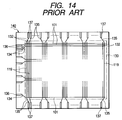
- Fig. 14 is a plan view showing a thin film transistor (hereinafter, referred to as TFT) array substrate 140.
- TFT thin film transistor
- a display area 130 in which pixel areas 132 constituting pixels are arranged in a matrix shape there are formed respectively: a display area 130 in which pixel areas 132 constituting pixels are arranged in a matrix shape; leader wiring 134 and scanning line terminals 136 for scanning lines for connecting scanning lines 101 in this display area 130 to an external gate driver IC; and leader wiring 135 and signal line terminals 137 for signal lines for connecting signal lines 119 in the display area 130 to an external source driver IC.
- sub-display area aimed at displaying, for example, character information in addition to a display area 30 (hereinafter, referred to as main display area) as shown in Fig. 1.
- the pixel area 32 is made small, but in the sub-display area 31, it is not always necessary to cause the size of its pixel area 33 to coincide with that of the main display area because of the display object.
- design is made so as to cause the size of the pixel area 33 in the sub-display area 31 to be rather bigger than that of the pixel area 32 in the main display area 30.
- a liquid crystal layer is pinched between a pair of substrates oppositely arranged, and this liquid crystal layer is used as a display medium.
- AC voltage in which DC voltage is not superimposed is applied to the liquid crystal layer, and this is used as display voltage.
- This AC voltage is applied to a pixel electrode mainly constituting the pixel area from the signal line through TFT which has turned ON through gate voltage from the scanning line.
- a steady DC voltage is applied to an opposite electrode which opposes to this pixel electrode through the liquid crystal layer.
- an electric field is imparted to the liquid crystal layer to change its refractive index whereby the liquid crystal layer becomes usable as a display medium.
- a dynamic voltage drop ⁇ Vp occurs in potential Vp of the pixel electrode when the gate voltage is changed in order to cause TFT to be in an OFF state, resulting from: a change in the dielectric constant of the liquid crystal in response to the field intensity; existence of parasitic capacity between gate electrode and drain electrode of TFT; existence of parasitic capacity between scanning line and pixel electrodes sandwiching insulating film therebetween; existence of parasitic capacity between scanning line and capacity electrodes sandwiching insulating film therebetween; existence of parasitic capacity between signal line and pixel electrodes sandwiching insulating film therebetween; existence of parasitic capacity between signal line and capacity electrodes sandwiching insulating film therebetween; and the like.
- Variations in the dielectric constant of the liquid crystal, which is one factor for causing the voltage drop, in response to the field intensity relate to the physical properties of the liquid crystal and cannot be avoided. Also, as the other factor, there are parasitic capacity of circuits, of which, existence of parasitic capacity between gate electrode and drain electrode of TFT cannot be structurally avoided in the current active matrix type liquid crystal display because gate insulating film formed between the electrodes forms capacity.
- the potential at the opposite electrode is adjusted at the optimum such that the positive and negative voltage amplitudes for AC voltage for driving the liquid crystal are equal to each other, and the storage capacity is formed in parallel with respect to the capacity of the liquid crystal layer, whereby an attempt has been made to resolve the flickers.
- the present invention has been achieved in order to solve the above-described problems, and is aimed to provide an active matrix type liquid crystal display capable of preventing flickers from occurring by applying the same potential to the opposite electrode without dividing the opposite electrode between main and sub-display areas which have pixel areas different in size respectively.
- An active matrix apparatus is constructed such that there is sandwiched a liquid crystal layer between a pair of substrates oppositely arranged; on the surface of one substrate, a plurality of scanning lines and a plurality of signal lines are formed to intersect each other in a matrix shape; in the vicinity of a plurality of intersected portions formed by the plurality of scanning lines and signal lines, there are formed respectively TFTs having gate electrodes connected to the scanning lines, pixel electrodes connected to the TFTs, and capacity electrodes for forming storage capacity with the scanning lines and the storage capacity; on the surface of the other substrate on the liquid crystal layer side, there is formed an opposite electrode; there are provided a main display area having a plurality of pixel areas, each of the pixel areas being enclosed with the scanning lines and the signal lines and being equal to one another, and a sub-display area having pixel areas different in size from the pixel areas in the main display area having the plurality of pixel areas; and a ratio of minimum space between each pixel electrode, the scanning line for driving it
- Cgd varies depending upon the channel width W and channel length L of the TFT, but a ratio of the minimum space between pixel electrode, scanning line and gate electrode, to the maximum space between opposite surfaces of the paired substrates is set to one or more. If Cgd cannot be ignored, ⁇ Vp cannot be designed by handling each of them as an independent parameter because Cgp also varies with Cgd. For this reason, since it becomes possible according to such a liquid crystal display to ignore the Cgp, it becomes easy to design the ⁇ Vp, and it is possible to design such that the main and sub-display areas having pixel areas different in size respectively have ⁇ Vp in common, and therefore, to make potential at the opposite electrodes identical.
- a maximum space between each pixel electrode, scanning line for driving it and gate electrode in the sub-display area is preferably set to a smaller value than a value obtained by deducting the length of the pixel electrode in the main display area in a direction perpendicular to the scanning line thereof from the length of the pixel electrode in the sub-display area in a direction perpendicular to the scanning lines thereof. This is because it becomes possible to make the potential at the opposite electrodes identical for the above reason, and the aperture ratio of the sub-display area is made larger than that of the main display area.
- Another active matrix type liquid crystal display according to the present invention adopts, in an active matrix type liquid crystal display having main and sub-display areas having pixel areas different in size respectively, means for preventing flickers and sticking from occurring by making voltage drop ⁇ Vp of the pixel electrode equal to each other between the main and sub-display areas with respect to the identical opposite electrode potential without dividing the opposite electrode.
- an active matrix type liquid crystal display in which there is sandwiched a liquid crystal layer between a pair of substrates oppositely arranged; on the surface of the one substrate, a plurality of scanning lines and a plurality of signal lines are formed to intersect each other in a matrix shape; in the vicinity of a plurality of intersected portions formed by the scanning lines and signal lines, there are formed respectively: TFTs having gate electrodes connected to the scanning lines, pixel electrodes connected to the TFTs through drain electrodes, and capacity electrodes for forming storage capacity with the scanning lines; and there are constituted a main display area and a sub-display area having pixel areas different from each other in size respectively, each of the pixel areas being enclosed with the scanning lines and signal lines, while on the surface of the other opposite substrate on the liquid crystal layer side, there is formed an opposite electrode, wherein there is adopted, as one means, a method for changing the storage capacity of the TFTs by making the channel widths of the TFTs different between the main and sub-
- the capacity Clc of liquid crystal layer As shown in the equation (1), as factors for causing the voltage drop ⁇ Vp of potential at pixel electrode, the capacity Clc of liquid crystal layer, the parasitic capacity Cgd of TFT, the storage capacity Cs and the like are included.
- the voltage drop ⁇ Vp becomes smaller.
- the parasitic capacity Cgp between the scanning lines and the pixel electrode is capacity to be formed by a non-uniform electric field, and therefore, it is difficult to adjust the value in design.
- the parasitic capacity Cgd of the TFT can be made smaller or the storage capacity Cs can be made larger.
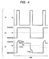
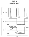
- a fluctuation ⁇ Vp in the pixel electrode potential depends also upon fall delay time of the gate signal.
- the gate voltage is cut off to cause the TFT to be in an OFF state in Fig. 6(a)
- the voltage is not cut off in an acute-angled rectangle shape as indicated by solid line, but exponentially fluctuates as indicated by broken line to generate delay time (t) before the voltage disappears.
- the fall delay time (t) of the gate signal is large, the TFT will not become completely OFF, and therefore, electric charge leaks from the pixel electrode through the TFT to cause the fluctuation in the pixel potential.
- the voltage were cut off originally like an acute angle when the gate signal is caused to be in an OFF-state, such ⁇ Vp as indicated by solid line would occur in Fig.
- the delay of the scanning signal affecting the voltage drop ⁇ Vp of the pixel electrode is determined by the wiring resistance and wiring capacity of the scanning lines. Assuming the wiring resistance of the scanning lines to be Rg and the wiring capacity thereof to be Cg, a time constant T of the scanning lines is expressed as the product of Rg and Cg.
- T Rg ⁇ Cg
- T represents delay in the scanning signal, if both areas are equal in time constant T irrespective of the size of the pixel area, they will also become equal in signal delay, and accordingly also in ⁇ Vp' of Fig. 6(c).
- the Cg changes, and the time constant also changes. Accordingly, as a countermeasure against flickers in a liquid crystal display having main and sub-display areas having pixel areas different in size, there is posed a problem how time constants T of each display area should be made equal to each other.
- the Rg and Cg are values obtained by composing all resistance and capacity connected to the scanning lines respectively.
- wiring resistance is included in wiring resistance of the scanning lines themselves and the leader wiring.
- the main and sub-display areas are caused to have the fall delay time (t) of the gate voltage in common, and to have voltage amplitudes, in common, due to positive and negative polarities without changing the potential at the opposite electrode.
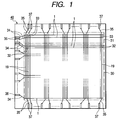
- Fig. 1 shows a TFT array substrate 40 in an active matrix type liquid crystal display according to a first embodiment of the present invention.
- a main display area 30 in which pixel areas 32 constituting pixels are arranged in a matrix shape, and a sub-display area 31 in which pixel areas 33 similarly constituting pixels are arranged in a matrix shape.
- Scanning lines 1 for scanning these pixel areas and signal lines 19 for supplying signals are formed in a lattice shape.
- the signal lines 19 are continuously wired without being discontinued between the main display area 30 and the sub-display area 31, which are different in size of pixel area.
- the sub-display area 31 consisting of pixel areas 33, each of which is larger in size than each of the pixel areas 32 in the main display area 30, is formed in the upper part of the main display area 30 such that the widths of the pixel areas coincide with each other in a direction in which the signal lines 19 extend. More specifically, the pixel area in the main display area 30 has size of 40 ⁇ m in width ⁇ 120 ⁇ m in length while the pixel area in the sub-display area 31 has size of 40 ⁇ m in width ⁇ 400 ⁇ m in length.
- leader wiring 34 of the scanning lines 1 brought out from the scanning lines 1 of each display area 30, 31 to terminals 36 of the scanning lines 1 for connecting to external gate driver IC and leader wiring 35 of the signal lines 19 brought out from the signal lines 19 of each display area 30, 31 to terminals 37 of the signal lines 19 for connecting to external source driver IC.
- leader wiring 34 from the scanning lines 1 and the leader wiring 35 from the signal lines 19 may be brought out to the output from this driving circuit.
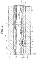
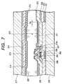
- an opposite substrate 17 arranged to oppose to a substrate 16 for constituting a TFT array substrate 40 through a liquid crystal layer 20 is, as shown in Fig. 2, provided with a light-shielding black matrix 15, a color filter 14, and a transparent opposite electrode 13 made of indium tin oxide, similar to a pixel electrode 11.
- orientation film 12 is formed on a surface in contact with the liquid crystal. Therefore, when voltage is applied between the pixel electrode 11 and the opposite electrode 13, it is arranged such that an electric field is applied to the liquid crystal layer 20, and that orientation control of liquid crystal molecules can be performed.
- This structure can be regarded as capacity (hereinafter, referred to as liquid crystal capacity) because it has the pixel electrode 11 and the opposite electrode 13 respectively as electrode, and has a liquid crystal, which is dielectric, therebetween.
- the TFT is, as shown in Figs. 2 and 3, formed by providing a gate electrode 2 provided by bringing out of the scanning lines 1, providing, on top thereof, gate insulating film 3 made of silicon nitride, providing, on top thereof, semiconductor film 4 made of amorphous silicon, further providing, on top thereof, ohmic film 5 made of n+ type amorphous silicon obtained by adding phosphorus to the amorphous silicon, and by providing, on top thereof, a drain electrode 7 and a source electrode 8 which are made of conductive material.
- the source electrode 8 is provided by bringing out of the signal lines 19.
- passivation film 10 made of silicon nitride is provided so as to cover these, the passivation film 10 on the drain electrode 7 is formed with a contact hole 18a, and thereafter, there is provided a transparent pixel electrode 11 made of indium tin oxide so as to connect through the drain electrode 7 and the contact hole 18a.
- Storage capacity is formed with the scanning lines 1 as one electrode, with the gate insulating film 3 on top thereof as dielectric, and further on top thereof, with a capacity electrode 9 of storage capacity made of conductive material of the same layer as the drain electrode 7 and the source electrode 8 as the other electrode.
- passivation film 10 is formed as in the case of the TFT.
- the pixel electrode 11 is provided by bringing it out above the capacity electrode 9, and the capacity electrode 9 and the pixel electrode 11 are connected through the contact hole 18b.
- the storage capacity is in parallel connection with the above-described liquid crystal capacity, and both become load capacity of the TFT.
- two pixel areas having size of 40 ⁇ m in width ⁇ 120 ⁇ m in length and size of 40 ⁇ m in width ⁇ 400 ⁇ m in length respectively are formed on the same TFT array substrate 40.
- the pixel area 33 of the sub-display area 31 having size of 40 ⁇ m ⁇ 400 ⁇ m, which is larger in pixel area size the design has been made such that, as shown in Figs.
- minimum space Db between the scanning line 1 and the pixel electrode 11 is larger than maximum space d between the substrate 16 and the opposite substrate 17, which are oppositely arranged, and that the minimum space Db becomes smaller than a value obtained by deducting length of the pixel electrode 211 of the main display area 30 in a direction perpendicular to scanning lines 201 in the main display area 30 from length of the pixel electrode 11 of the sub-display area 31 in a direction perpendicular to the scanning lines 1 in the sub-display area 31.
- the design was made such that the space between the scanning lines 1 and the pixel electrode 11 becomes 8 ⁇ m while the space between these substrates oppositely arranged is 4 ⁇ m. This enables reducing the parasitic capacity between the scanning lines 1 and the pixel electrode 11.
- TFT consisting of a gate electrode 202 brought out from the scanning lines 201, a semiconductor layer 204, and a source electrode 208 and a drain electrode 207 brought out from the signal lines 219; a pixel electrode 211 connected to the drain electrode 207 of this TFT through the contact hole 218a; and storage capacity having a capacity electrode 209 formed in the same layer as signal lines 219 and the scanning lines 201 as opposite electrodes.
- a ratio of the minimum space Db between the pixel electrode 11, the scanning line 1 and the gate electrode 2 in the sub-display area 31, to the maximum space d between the opposite surfaces of the substrate is set to one or more so as to be able to ignore Cgp, which is a design parameter of ⁇ Vp as described above, whereby a design equation for ⁇ Vp can be simplified. For this reason, by adjusting values of Cgdon and Cgdoff which depend upon dimensions of Cs, channel length and channel width of the TFT, it becomes easy to design ⁇ Vp in the main display area 30 and the sub-display area 31 to be equal to each other.
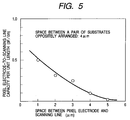
- Fig. 5 is a view showing relationship between space between the scanning line 1 and the pixel electrode 11, and parasitic capacity between the scanning line 1 and the pixel electrode 11 when the maximum space between opposite surfaces of the pair of substrates 16 and 17 oppositely arranged is, in the present embodiment shown in Fig. 3, set to 4 ⁇ m.
- the parasitic capacity of the TFT is 10PF according to the present embodiment, it can be seen according to the result of Fig. 5 that if the maximum space between opposite surfaces of the pair of substrates 16 and 17 oppositely arranged is set to 4 ⁇ m, the parasitic capacity between the scanning line 1 and the pixel electrode 11 can be converted to about 0.
- the minimum space between the scanning lines 1 and the pixel electrode 11 has been designed to be 8 ⁇ m allowing for sufficient room. According to the result of Fig. 5, it can be seen that the parasitic capacity could be ignored if there is provided the space of 4 ⁇ m or more, which is the maximum space between opposite surfaces of the pair of substrates 16 and 17 oppositely arranged, or more. This can be easily understood because a line of electric force extending from the scanning lines given with electric potential is terminated toward an electrode located at a minimum distance therefrom, and capacity is formed by charge to be appeared at both ends of the line of electric force.
- Fig. 9 is a plan view showing a TFT array substrate 340 in an active matrix type liquid crystal display according to the second embodiment of the present invention.
- a multiplicity of pixel areas 332 and 333 are arranged in a matrix shape on a main display area 330 and a sub-display area 331 respectively.
- the pixel area is an area enclosed with scanning lines 301 and signal lines 319, and pixel areas located in the main display area 330 and the sub-display area 331 are different in size.
- the pixel area 332 in the main display area 330 has size of 40 ⁇ m in width ⁇ 120 ⁇ m in length
- the pixel area 333 in the sub-display area 331 has size of 40 ⁇ m in width ⁇ 400 ⁇ m in length.
- the sub-display area 331 consisting of pixel areas 333, each of which is larger in size than each of the pixel areas 332 in the main display area 330, is formed in the upper part of the main display area 330 such that the widths of the pixel areas coincide with each other in a scanning line direction.
- Scanning lines 301 for scanning these pixel areas and signal lines 319 for supplying signals are formed in a lattice shape.
- the signal lines 319 are not discontinued between the main display area 330 and the sub-display area 331 which are different from each other in size of pixel area, but are continuously wired.
- leader wiring from the scanning lines and the leader wiring from the signal lines may be brought out to the output from this driving circuit.
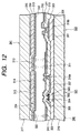
- Fig. 10 is an enlarged plan view for one pixel area 333 in the sub-display area 331 of the liquid crystal display according to the present embodiment.
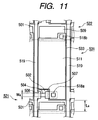
- Fig. 11 is an enlarged plan view for one pixel area 332 in the main display area 330.
- Fig. 12 is a sectional view taken on line A-A' which penetrates the TFT, contact hole and capacity electrode of Fig. 10.
- the pixel area 332 of the main display area 330 is also different only in size of pixel area, channel width of TFT and dimension of storage capacity, and has the same structure as the pixel area 333 of the sub-display area 331.
- the pixel area 333 in the sub-display area 331 is enclosed with scanning lines and signal lines, and in the lower left of the plane, TFT 321 is formed, and in the upper portion of the plane, storage capacity 322 is formed. In the central portion thereof, a pixel electrode 311 is arranged.
- the liquid crystal display using the TFT array substrate 340 has, as shown in Fig. 12, an opposite substrate 341 arranged to oppose to the TFT array substrate 340 through a liquid crystal layer 320.
- the opposite substrate 341 is provided with a light-shielding black matrix 315, a color filter 314, and a transparent opposite electrode 313 made of indium tin oxide (hereinafter, abbreviated as ITO), similar to an pixel electrode 311.
- ITO indium tin oxide
- orientation film 312 is formed on a surface in contact with the liquid crystal. Therefore, when voltage is applied between the pixel electrode 311 and the opposite electrode 313, it is arranged such that an electric field is applied to the liquid crystal layer 320, and that orientation control of liquid crystal molecules can be performed.
- This structure can be regarded as capacity (hereinafter, referred to as liquid crystal capacity) because it has the pixel electrode 311 and the opposite electrode 313 respectively as electrode, and has a liquid crystal layer 320, which is dielectric, therebetween.
- the TFT is, as shown in Figs. 10 and 12, formed by providing a gate electrode 302 provided by bringing out from the scanning lines 301, providing, on top thereof, gate insulating film 303 made of silicon nitride, providing, on top thereof, semiconductor film 304 made of amorphous silicon, further providing, on top thereof, ohmic contact film 305 made of n+ type amorphous silicon obtained by adding phosphorus to the amorphous silicon, and providing, on top thereof, a drain electrode 307 and a source electrode 308 which are made of conductive material.
- the source electrode 308 is provided by bringing out from the signal lines 319.
- passivation film 310 made of silicon nitride is provided so as to cover these, the passivation film 310 on the drain electrode 307 is formed with a contact hole 318a.
- the drain electrode 307 and a transparent pixel electrode 311 made of ITO are connected together through the contact hole 318a.
- Storage capacity 322 is formed with the scanning lines 301 as one electrode and with the gate insulating film 303 on top thereof as dielectric, and further on top thereof, a capacity electrode 309 serving as the other electrode is formed.
- the capacity electrode 309 is formed by the same conductive material as the drain electrode 307 and the source electrode 308.
- passivation film 310 is formed as in the case of the TFT 321.
- a contact hole 318b is formed, a pixel electrode 311 made of ITO is provided by bringing it out on the capacity electrode 309, and the capacity electrode 309 and the pixel electrode 311 are connected together through the contact hole 318b.
- the storage capacity 322 is in parallel connection with the above-described liquid crystal capacity, and both become load capacity of the TFT 321.
- the pixel area 332 in the main display area 330 has size of 40 ⁇ m in width ⁇ 120 ⁇ m in length
- the pixel area 333 in the sub-display area 331 has size of 40 ⁇ m in width ⁇ 400 ⁇ m in length.
- the pixel area 332 in the main display area 330 is smaller, and the pixel area 333 in the sub-display area 331 is larger. Therefore, in order to make the voltage drop ⁇ Vp in each pixel electrode equal to each other, the parasitic capacity Cgd of the TFT in the sub-display area 331 can be made larger or the storage capacity Cs can be made smaller by making the parasitic capacity Cgdon of the TFT in the main display area 330 smaller or making the storage capacity Cs larger as described above.
- the parasitic capacity Cgd of the TFT is determined by the area of a portion where the gate electrode, the semiconductor film (channel) and the drain electrode of the TFT overlap one another. To shorten the channel length is restrained by the design rule, and to lengthen the channel length deteriorates the current driving capacity of the TFT, and therefore, they are not advisable. Accordingly, the channel width will be adjusted. In Figs. 10 and 11, the width Wa, Wb of the semiconductor film 304 is the channel width. In the main display area 330 having a smaller pixel area, the channel width is made narrower, and conversely, in the sub-display area 331 having a larger pixel area, the channel width is made wider.
- the channel length is both set to 3 ⁇ m, and the channel width in the main display area is set to 5 ⁇ m, and the channel width in the sub-display area is set to 29 ⁇ m.
- the storage capacity Cs is determined by areas for storage electrodes 309 and 509 formed on scanning lines 301 and 501 in Figs. 10 and 11. Length of the storage electrodes 309 and 509 is determined by size of the pixel because the storage electrodes 309 and 509 are enclosed with signal lines 319 and 519 respectively. Therefore, the area is adjusted by changing the width of the storage electrode 309 or 509. The storage capacity Cs also changes in proportion to the area.
- the storage capacity for the main display area is set to 216 PF
- the storage capacity for the sub-display area is set to 523 PF.
- the wiring resistance of the scanning lines includes wiring resistance of the scanning lines themselves within the display area, and wiring resistance of leader wiring of the scanning lines in the panel portion outside the display area.
- the size of the pixel area is smaller in the main display area, and is larger in the sub-display area. Accordingly, the capacity of the liquid crystal layer is also smaller in the main display area, and is larger in the sub-display area. Therefore, since the capacity Cg of the scanning lines becomes smaller in the main display area, and is larger in the sub-display area from the above-described equation (3), delay time of the scanning signal also becomes smaller in the main display area, and is larger in the sub-display area. In such a case, in order to make the delay time T constant, the wiring resistance Rg of the scanning lines can be made larger in the main display area, and conversely smaller in the sub-display area from the equation (2).
- the wiring resistance Rg of the scanning lines there are several methods.
- As the wiring resistance Rg of the scanning lines there are resistance of the scanning lines within the display area shown in Fig. 9, and resistance of leader wiring for connecting from the display area to the terminal of the scanning lines for connecting to the gate driver IC. These wiring resistance can be made larger in the main display area and smaller in the sub-display area.
- the width of the scanning lines is changed assuming the thickness of the wiring to be constant because the length of the scanning lines is determined by the size of the display area.
- the width of the scanning line within the display area can be made narrower in the main display area and wider in the sub-display area.
- the width La of the scanning lines 501 in the main display area is 31 ⁇ m
- the width Lb of the scanning lines 1 in the sub-display area is set to 86 ⁇ m. This enables signal delay time in the scanning lines in the main and sub-display areas to become equal to each other.
- the description will be made of a method for adjusting the resistance of leader wiring for connecting from the display area to the terminals of the scanning lines for connecting to the gate driver IC.
- the wiring resistance of the larger pixel area side is made smaller as described above.
- Scanning line terminals are, as shown in Fig. 9, provided in space in the panel portion of the liquid crystal display. Therefore, some degree of freedom is left in design for leader wiring from the display area to the terminals within a range of the space in the panel portion.
- means for changing the length or width of the wiring can be adopted. If the wiring length is made longer, the wiring resistance Rg becomes higher, and the wiring resistance Rg can become higher even by making the wiring width narrower.
- the wiring resistance Rg can be adjusted by changing at least one or both of the length and width of the wiring. If the width is made narrower, the wiring resistance becomes higher, and if the length is made longer, the wiring resistance becomes higher. Therefore, the width and length can be adjusted in consideration of the space in the panel portion.
- the width and length of the leader wiring 334a of the main display area are set to 15 ⁇ m and 4mm respectively, and the width and length of the leader wiring 334b of the sub-display area are set to 30 ⁇ m and 3mm respectively. This enables signal delay time in the scanning lines in the main and sub-display areas to become equal to each other.
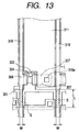
- scanning lines 301 and signal lines 319 are constituted so as to surround the pixel electrode 311 in the sub-display area 331 as shown in Fig. 13.
- the scanning lines 301 and the signal lines 319 intersect each other. Since the scanning lines 301 and the signal lines 319 overlap each other through insulating film in this intersected portion, wiring capacity Cx is to be formed.
- a gate electrode 302 on top of which there are provided a TFT and storage capacity, and the storage capacity is connected to a neighboring pixel electrode 311. Therefore, these capacity is to constitute series capacity on top of the scanning lines 301.
- the wiring capacity Cg of the scanning lines is given by equation (3).
- the scanning lines 301 are wired so as to place the pixel areas in a row within each display area, and the signal lines 319 are continuously wired throughout the main and sub-display areas.
- An area S of the portion where the scanning lines 301 and the signal lines 319 overlap each other is an area of the portion indicated by hatching in Fig. 13, represented by width W and L. Therefore, the area S can be changed by changing the width W of the signal lines or the width L of the scanning lines in the intersected portion. Or, the area S of the overlapped portion can be changed by changing both the width W and L.
- the pixel area is small in size, and the capacity Clc of the liquid crystal layer is small. Therefore, in order to make Cg constant in the equation (3), the area of the overlapped portion of the scanning lines 301 and signal lines 319 can be made smaller to make Cx smaller.
- the width L of the scanning lines 301 is set to 31 ⁇ m
- the width W of the signal lines 319 is set to 3 ⁇ m, that is, the area Sa of the overlapped portion is set to 93 ⁇ m 2
- the width L of the scanning lines 1 is set to 86 ⁇ m
- the width W of the signal lines 319 is set to 3 ⁇ m, that is, the area Sb of the overlapped portion is set to 258 ⁇ m 2 .
- an active matrix type liquid crystal display according to the present invention is capable of preventing flickers and sticking by applying optimum opposite substrate potential to one opposite electrode without dividing an opposite electrode to apply optimum DC voltage to the respective ones.
- another active matrix type liquid crystal display is capable of making delay time of a gate signal equal to each other between the main and sub-display areas having different pixel areas in size respectively, and making voltage drop ⁇ Vp of the pixel electrode equal to each other. As a result, it is possible to prevent flickers and sticking in a simple structure without dividing the opposite electrode and without changing the opposite electrode voltage, and to obtain excellent quality display images.
Landscapes
- Physics & Mathematics (AREA)
- Nonlinear Science (AREA)
- Optics & Photonics (AREA)
- Crystallography & Structural Chemistry (AREA)
- Chemical & Material Sciences (AREA)
- General Physics & Mathematics (AREA)
- Mathematical Physics (AREA)
- Engineering & Computer Science (AREA)
- Microelectronics & Electronic Packaging (AREA)
- Power Engineering (AREA)
- Geometry (AREA)
- Liquid Crystal (AREA)
- Liquid Crystal Display Device Control (AREA)
Abstract
Description
Claims (15)
- An active matrix type liquid crystal display wherein there is sandwiched a liquid crystal layer between a pair of substrates oppositely arranged; on the surface of the one substrate, a plurality of scanning lines and a plurality of signal lines are formed to intersect one another in a matrix shape; in the vicinity of a plurality of intersected portions formed by the plurality of scanning lines and signal lines, there are formed respectively thin film transistors (hereinafter, referred to as TFTs) having gate electrodes connected to the scanning lines, pixel electrodes connected to the TFTs, and capacity electrodes for forming storage capacity with the scanning lines; on the surface of the other substrate on the liquid crystal layer side, there is formed an opposite electrode; there are provided a main display area having a plurality of pixel areas, each of the pixel areas being enclosed with the scanning lines and the signal lines and being equal to one another in size, and a sub-display area having pixel areas different, in size, from the pixel areas in the main display area having the plurality of pixel areas; and a ratio of minimum space between each pixel electrode, the scanning line for driving it and the gate electrode in the sub-display area, to maximum space between opposite surfaces of the paired substrates is set to one or more.
- An active matrix type liquid crystal display according to Claim 1 wherein maximum space between each pixel electrode, the scanning line for driving it and the gate electrode in the sub-display area is set to a smaller value than a value obtained by deducting length of the pixel electrode in the main display area in a direction perpendicular to the scanning line thereof from length of the pixel electrode in the sub-display area in a direction perpendicular to the scanning line thereof.
- An active matrix type liquid crystal display wherein there is sandwiched a liquid crystal layer between a pair of substrates oppositely arranged; on the surface of one of the substrates, a plurality of scanning lines and a plurality of signal lines are formed to intersect each other in a matrix shape; in the vicinity of a plurality of intersected portions formed by the plurality of scanning lines and signal lines, there are formed respectively TFTs having gate electrodes connected to the scanning lines, pixel electrodes connected to the TFTs through drain electrodes, and storage capacity; there are provided a main display area and a sub-display area which have pixel areas different from each other in size respectively, each of the pixel areas being enclosed with the scanning lines and the signal lines; all around each display area, there are formed leader wiring for the scanning lines and leader wiring for the signal lines; on the surface of the other opposite substrate on the liquid crystal layer side, there is formed an opposite electrode; and of first structure in which wiring resistance of the scanning lines in the main display area is different from wiring resistance of the scanning lines in the sub-display area,second structure in which an area of a portion where the scanning lines and the signal lines overlap in the main display area is different from an area of a portion where the scanning lines and the signal lines overlap in the sub-display area,third structure in which a channel width of TFT in the main display area is different from a channel width of TFT in the sub-display area, andfourth structure in which storage capacity of the main display area is different from storage capacity of the sub-display area, the active matrix type liquid crystal display has any one structure.
- An active matrix type liquid crystal display according to Claim 3 wherein a width of the scanning line in the main display area is different from a width of the scanning line in the sub-display area.
- An active matrix type liquid crystal display according to Claim 3 or 4 wherein the pixel area in the main display area is smaller in size than the pixel area in the sub-display area.
- An active matrix type liquid crystal display according to Claim 5 wherein the pixel area in the main display area is smaller in size than the pixel area in the sub-display area and the scanning line in the main display area is narrower in width than the scanning line in the sub-display area.
- An active matrix type liquid crystal display according to any Claim 3 to 6 wherein the active matrix type liquid crystal display is constructed such that at least one of a width or length of the leader wiring of the scanning line in the main display area is different from a width or length of the leader wiring of the scanning line in the sub-display area.
- An active matrix type liquid crystal display according to Claim 7 wherein the active matrix type liquid crystal display is constructed such that the pixel area in the main display area is smaller in size than the pixel area in the sub-display area, and that at least one of a width or length of the leader wiring of the scanning line in the main display area is narrower or longer than a width or length of the leader wiring of the scanning line in the sub-display area.
- An active matrix type liquid crystal display according to Claim 3 wherein the active matrix type liquid crystal display is constructed such that both the width and length of the leader wiring of the scanning line in the main display area are different from both the width and length of the leader wiring of the scanning line in the sub-display area respectively.
- An active matrix type liquid crystal display according to Claim 9 wherein the pixel area in the main display area is smaller in size than the pixel area in the sub-display area, and wherein both the width and length of the leader wiring of the scanning line in the main display area are narrower and longer than the width and length of the leader wiring of the scanning line in the sub-display area respectively.
- An active matrix type liquid crystal display according to Claim 3 wherein the pixel area in the main display area is smaller in size than the pixel area in the sub-display area, and wherein an area of a portion where the scanning lines and the signal lines overlap in the main display area is smaller than an area of a portion where the scanning lines and the signal lines overlap in the sub-display area.
- An active matrix type liquid crystal display according to Claim 3 wherein the pixel area in the main display area is smaller in size than the pixel area in the sub-display area, and wherein the channel width of TFT in the main display area is narrower than the channel width of TFT in the sub-display area.
- An active matrix type liquid crystal display according to Claim 3 wherein the pixel area in the main display area is smaller in size than the pixel area in the sub-display area, and wherein storage capacity of the main display area is smaller than storage capacity of the sub-display area.
- An active matrix type liquid crystal display according to Claim 3 wherein the pixel area in the main display area is smaller in size than the pixel area in the sub-display area, wherein the channel width of TFT in the main display area is narrower than the channel width of TFT in the sub-display area, and wherein the storage capacity of the main display area is smaller than the storage capacity of the sub-display area.
- An active matrix type liquid crystal display wherein there is sandwiched a liquid crystal layer between a pair of substrates oppositely arranged; on the surface of one of the substrates, a plurality of scanning lines and a plurality of signal lines are formed to intersect each other in a matrix shape; in the vicinity of a plurality of intersected portions formed by the plurality of scanning lines and signal lines, there are formed respectively TFTs having gate electrodes connected to the scanning lines, pixel electrodes connected to the TFTs through drain electrodes, and storage capacity; there are provided a main display area and a sub-display area which have pixel areas different from each other in size respectively, each of the pixel areas being enclosed with the scanning lines and the signal lines; all around each display area, there are formed leader wiring for the scanning lines and leader wiring for the signal lines; on the surface of the other opposite substrate on the liquid crystal layer side, there is formed an opposite electrode; the pixel area in the main display area is smaller in size than the pixel area in the sub-display area; both the width and length of the leader wiring of the scanning line in the main display area are narrower and longer than the width and length of the leader wiring of the scanning line in the sub-display area respectively; an area of a portion where the scanning lines and the signal lines overlap in the main display area is smaller than an area of a portion where the scanning lines and the signal lines overlap in the sub-display area; the channel width of TFT in the main display area is narrower than the channel width of TFT in the sub-display area; and the storage capacity of the main display area is smaller than the storage capacity of the sub-display area.
Applications Claiming Priority (4)
| Application Number | Priority Date | Filing Date | Title |
|---|---|---|---|
| JP20168899A JP2001033811A (en) | 1999-07-15 | 1999-07-15 | Active matrix type liquid crystal display device |
| JP20168899 | 1999-07-15 | ||
| JP33205399 | 1999-11-22 | ||
| JP33205399A JP2001147448A (en) | 1999-11-22 | 1999-11-22 | Active matrix type liquid crystal display device |
Publications (2)
| Publication Number | Publication Date |
|---|---|
| EP1069463A2 true EP1069463A2 (en) | 2001-01-17 |
| EP1069463A3 EP1069463A3 (en) | 2004-08-04 |
Family
ID=26512931
Family Applications (1)
| Application Number | Title | Priority Date | Filing Date |
|---|---|---|---|
| EP00305778A Withdrawn EP1069463A3 (en) | 1999-07-15 | 2000-07-07 | Active matrix type liquid crystal display |
Country Status (3)
| Country | Link |
|---|---|
| US (1) | US6587174B1 (en) |
| EP (1) | EP1069463A3 (en) |
| KR (1) | KR100383294B1 (en) |
Cited By (1)
| Publication number | Priority date | Publication date | Assignee | Title |
|---|---|---|---|---|
| WO2003060868A1 (en) * | 2002-01-17 | 2003-07-24 | International Business Machines Corporation | Display device, scanning line driver circuit |
Families Citing this family (7)
| Publication number | Priority date | Publication date | Assignee | Title |
|---|---|---|---|---|
| KR100381868B1 (en) * | 2000-11-29 | 2003-05-01 | 삼성전자주식회사 | a liquid crystal display and a substrate for the same |
| KR100796749B1 (en) | 2001-05-16 | 2008-01-22 | 삼성전자주식회사 | Thin Film Transistor Array Board for Liquid Crystal Display |
| US7164684B2 (en) * | 2001-05-18 | 2007-01-16 | Ge Fanuc Automation North America, Inc. | Ethernet node having hub, switch and/or repeater characteristics |
| US7385223B2 (en) * | 2003-04-24 | 2008-06-10 | Samsung Sdi Co., Ltd. | Flat panel display with thin film transistor |
| KR100514180B1 (en) * | 2003-08-13 | 2005-09-13 | 삼성에스디아이 주식회사 | Current supply line structure in FPD |
| JP4490708B2 (en) * | 2003-09-18 | 2010-06-30 | シチズンホールディングス株式会社 | Display device |
| CN106991990A (en) * | 2017-05-27 | 2017-07-28 | 上海天马有机发光显示技术有限公司 | Display panel and display device |
Family Cites Families (18)
| Publication number | Priority date | Publication date | Assignee | Title |
|---|---|---|---|---|
| DE2619367A1 (en) * | 1976-04-30 | 1977-11-17 | Siemens Ag | LIQUID CRYSTAL DISPLAY WITH ADDITIONAL LIGHTING |
| JPS58221826A (en) * | 1982-06-18 | 1983-12-23 | Fujitsu Ltd | Composite liquid crystal display panel |
| US4812017A (en) * | 1987-12-28 | 1989-03-14 | General Electric Company | Pixel configuration to achieve a staggered color triad with insulated connection between third, split pixel electrodes |
| JPH06100757B2 (en) * | 1990-07-09 | 1994-12-12 | インターナシヨナル・ビジネス・マシーンズ・コーポレーシヨン | Liquid crystal display |
| JPH0534719A (en) | 1991-07-26 | 1993-02-12 | Sharp Corp | Active matrix display device |
| US6337954B1 (en) * | 1993-01-28 | 2002-01-08 | Nikon Corporation | Camera having a display unit including multiple display areas and a connector mounted parallel to said multiple display areas |
| JP2671772B2 (en) | 1993-09-06 | 1997-10-29 | 日本電気株式会社 | Liquid crystal display and its driving method |
| JPH07128640A (en) * | 1993-10-29 | 1995-05-19 | Sharp Corp | Ferroelectric liquid crystal display device |
| US5644415A (en) * | 1993-12-20 | 1997-07-01 | Casio Computer Co., Ltd. | Liquid crystal display device having wide field angle |
| TW262553B (en) * | 1994-03-17 | 1995-11-11 | Hitachi Seisakusyo Kk | |
| JP3866815B2 (en) * | 1996-03-27 | 2007-01-10 | セイコーエプソン株式会社 | LIQUID CRYSTAL PANEL SUBSTRATE, ITS MANUFACTURING METHOD, LIQUID CRYSTAL DEVICE, AND ELECTRONIC DEVICE |
| JP3659608B2 (en) * | 1996-08-05 | 2005-06-15 | シャープ株式会社 | Liquid crystal display |
| JPH1062821A (en) * | 1996-08-23 | 1998-03-06 | Seiko Epson Corp | Liquid crystal display |
| KR100257862B1 (en) * | 1997-07-31 | 2000-06-01 | 구본준, 론 위라하디락사 | In-plane switching mode liquid crystal display device |
| KR100476624B1 (en) * | 1997-12-31 | 2005-07-07 | 삼성전자주식회사 | Thin film transistor substrate for liquid crystal display device and manufacturing method thereof |
| JP3874950B2 (en) * | 1998-12-01 | 2007-01-31 | アルプス電気株式会社 | Image display device |
| KR100317621B1 (en) * | 1999-02-24 | 2001-12-22 | 구본준, 론 위라하디락사 | Liquid Crystal Display |
| JP3558934B2 (en) * | 1999-10-14 | 2004-08-25 | アルプス電気株式会社 | Active matrix type liquid crystal display |
-
2000
- 2000-07-07 EP EP00305778A patent/EP1069463A3/en not_active Withdrawn
- 2000-07-14 KR KR10-2000-0040444A patent/KR100383294B1/en not_active Expired - Fee Related
- 2000-07-14 US US09/616,868 patent/US6587174B1/en not_active Expired - Lifetime
Cited By (1)
| Publication number | Priority date | Publication date | Assignee | Title |
|---|---|---|---|---|
| WO2003060868A1 (en) * | 2002-01-17 | 2003-07-24 | International Business Machines Corporation | Display device, scanning line driver circuit |
Also Published As
| Publication number | Publication date |
|---|---|
| KR20010015333A (en) | 2001-02-26 |
| KR100383294B1 (en) | 2003-05-12 |
| EP1069463A3 (en) | 2004-08-04 |
| US6587174B1 (en) | 2003-07-01 |
Similar Documents
| Publication | Publication Date | Title |
|---|---|---|
| US7847914B2 (en) | Thin film transistor array panel and method for repairing liquid crystal display including the same | |
| US9685130B2 (en) | Display device | |
| KR100371757B1 (en) | Active matrix type liquid crystal display | |
| US20070182872A1 (en) | Multi-domain liquid crystal display and a thin film transistor substrate of the same | |
| US8441589B2 (en) | Pixel array structure | |
| CN1199082C (en) | Active array type LCD | |
| KR101707212B1 (en) | Liquid crsytal display | |
| JP2003091017A (en) | Color liquid crystal display | |
| US9625777B2 (en) | Liquid crystal display | |
| KR100593314B1 (en) | Liquid crystal display | |
| EP1069463A2 (en) | Active matrix type liquid crystal display | |
| KR20080018773A (en) | LCD Display | |
| WO2005036653A1 (en) | Thin film transistor, thin film transistor array panel, and display device | |
| US20140340623A1 (en) | Liquid crystal display | |
| JP4213356B2 (en) | Liquid crystal display | |
| KR20070059558A (en) | Liquid crystal display | |
| KR102426423B1 (en) | Display substrate and Liquid crystal display apparatus including the same | |
| US7072005B2 (en) | IPS LCD and repair method of cutting defective pixel electrode by forming window in capacitor storage circuit | |
| KR100895015B1 (en) | Liquid crystal display | |
| WO2003083566A1 (en) | A vertically aligned mode liquid crystal display | |
| JP3378678B2 (en) | Liquid crystal display | |
| KR20080026277A (en) | Thin film transistor substrate and its repair method | |
| KR101471144B1 (en) | Method of detecting storage voltage, display apparutus using the storage voltage and method of driving the display apparutus | |
| KR100828213B1 (en) | Thin film transistor liquid crystal display device and manufacturing method thereof | |
| JP2001033811A (en) | Active matrix type liquid crystal display device |
Legal Events
| Date | Code | Title | Description |
|---|---|---|---|
| PUAI | Public reference made under article 153(3) epc to a published international application that has entered the european phase |
Free format text: ORIGINAL CODE: 0009012 |
|
| AK | Designated contracting states |
Kind code of ref document: A2 Designated state(s): AT BE CH CY DE DK ES FI FR GB GR IE IT LI LU MC NL PT SE |
|
| AX | Request for extension of the european patent |
Free format text: AL;LT;LV;MK;RO;SI |
|
| RIC1 | Information provided on ipc code assigned before grant |
Ipc: 7G 02F 1/1343 A |
|
| PUAL | Search report despatched |
Free format text: ORIGINAL CODE: 0009013 |
|
| RIC1 | Information provided on ipc code assigned before grant |
Ipc: 7G 02F 1/1368 B Ipc: 7G 02F 1/1343 A |
|
| AK | Designated contracting states |
Kind code of ref document: A3 Designated state(s): AT BE CH CY DE DK ES FI FR GB GR IE IT LI LU MC NL PT SE |
|
| AX | Request for extension of the european patent |
Extension state: AL LT LV MK RO SI |
|
| 17P | Request for examination filed |
Effective date: 20041022 |
|
| AKX | Designation fees paid |
Designated state(s): DE FR GB NL |
|
| RBV | Designated contracting states (corrected) |
Designated state(s): DE FR GB NL |
|
| 17Q | First examination report despatched |
Effective date: 20070726 |
|
| STAA | Information on the status of an ep patent application or granted ep patent |
Free format text: STATUS: THE APPLICATION IS DEEMED TO BE WITHDRAWN |
|
| 18D | Application deemed to be withdrawn |
Effective date: 20071206 |