EP1069456B1 - Electroabsorption optical modulator and fabrication method thereof - Google Patents
Electroabsorption optical modulator and fabrication method thereof Download PDFInfo
- Publication number
- EP1069456B1 EP1069456B1 EP00115143A EP00115143A EP1069456B1 EP 1069456 B1 EP1069456 B1 EP 1069456B1 EP 00115143 A EP00115143 A EP 00115143A EP 00115143 A EP00115143 A EP 00115143A EP 1069456 B1 EP1069456 B1 EP 1069456B1
- Authority
- EP
- European Patent Office
- Prior art keywords
- layer
- optical
- cladding layer
- upper cladding
- type
- Prior art date
- Legal status (The legal status is an assumption and is not a legal conclusion. Google has not performed a legal analysis and makes no representation as to the accuracy of the status listed.)
- Expired - Lifetime
Links
- 230000003287 optical effect Effects 0.000 title claims description 84
- 238000004519 manufacturing process Methods 0.000 title description 8
- 238000000034 method Methods 0.000 title description 6
- 238000010521 absorption reaction Methods 0.000 claims description 35
- 239000012535 impurity Substances 0.000 claims description 35
- 238000009792 diffusion process Methods 0.000 claims description 32
- 239000004065 semiconductor Substances 0.000 claims description 26
- 230000002401 inhibitory effect Effects 0.000 claims description 22
- 239000000463 material Substances 0.000 claims description 2
- 238000005253 cladding Methods 0.000 claims 14
- 150000001875 compounds Chemical class 0.000 claims 2
- 239000002019 doping agent Substances 0.000 claims 1
- 239000002245 particle Substances 0.000 claims 1
- 239000010410 layer Substances 0.000 description 168
- VYPSYNLAJGMNEJ-UHFFFAOYSA-N Silicium dioxide Chemical compound O=[Si]=O VYPSYNLAJGMNEJ-UHFFFAOYSA-N 0.000 description 44
- 229910052681 coesite Inorganic materials 0.000 description 22
- 229910052906 cristobalite Inorganic materials 0.000 description 22
- 239000000377 silicon dioxide Substances 0.000 description 22
- 229910052682 stishovite Inorganic materials 0.000 description 22
- 229910052905 tridymite Inorganic materials 0.000 description 22
- 239000000758 substrate Substances 0.000 description 16
- 229910000530 Gallium indium arsenide Inorganic materials 0.000 description 14
- 230000005684 electric field Effects 0.000 description 8
- 238000000206 photolithography Methods 0.000 description 8
- 230000008033 biological extinction Effects 0.000 description 6
- 230000003405 preventing effect Effects 0.000 description 6
- 239000011241 protective layer Substances 0.000 description 6
- 238000002230 thermal chemical vapour deposition Methods 0.000 description 5
- RBFQJDQYXXHULB-UHFFFAOYSA-N arsane Chemical compound [AsH3] RBFQJDQYXXHULB-UHFFFAOYSA-N 0.000 description 4
- HQWPLXHWEZZGKY-UHFFFAOYSA-N diethylzinc Chemical compound CC[Zn]CC HQWPLXHWEZZGKY-UHFFFAOYSA-N 0.000 description 4
- PZPGRFITIJYNEJ-UHFFFAOYSA-N disilane Chemical compound [SiH3][SiH3] PZPGRFITIJYNEJ-UHFFFAOYSA-N 0.000 description 4
- 238000005530 etching Methods 0.000 description 4
- RGGPNXQUMRMPRA-UHFFFAOYSA-N triethylgallium Chemical compound CC[Ga](CC)CC RGGPNXQUMRMPRA-UHFFFAOYSA-N 0.000 description 4
- IBEFSUTVZWZJEL-UHFFFAOYSA-N trimethylindium Chemical compound C[In](C)C IBEFSUTVZWZJEL-UHFFFAOYSA-N 0.000 description 4
- 230000004888 barrier function Effects 0.000 description 3
- 238000004891 communication Methods 0.000 description 3
- XYFCBTPGUUZFHI-UHFFFAOYSA-N Phosphine Chemical compound P XYFCBTPGUUZFHI-UHFFFAOYSA-N 0.000 description 2
- 229910007264 Si2H6 Inorganic materials 0.000 description 2
- 229910000070 arsenic hydride Inorganic materials 0.000 description 2
- 238000003486 chemical etching Methods 0.000 description 2
- 238000010030 laminating Methods 0.000 description 2
- 239000002994 raw material Substances 0.000 description 2
- 239000011701 zinc Substances 0.000 description 2
- HPGPZOQQVAAHLM-UHFFFAOYSA-N [CH-]1C=CC=C1.[CH-]1C=CC=C1.[Fe+2].C1(C=CC=C1)[Fe]C1C=CC=C1 Chemical compound [CH-]1C=CC=C1.[CH-]1C=CC=C1.[Fe+2].C1(C=CC=C1)[Fe]C1C=CC=C1 HPGPZOQQVAAHLM-UHFFFAOYSA-N 0.000 description 1
- 230000015572 biosynthetic process Effects 0.000 description 1
- 239000013078 crystal Substances 0.000 description 1
- 230000001419 dependent effect Effects 0.000 description 1
- 239000003989 dielectric material Substances 0.000 description 1
- 238000009826 distribution Methods 0.000 description 1
- 238000010438 heat treatment Methods 0.000 description 1
- 230000010365 information processing Effects 0.000 description 1
- 238000010884 ion-beam technique Methods 0.000 description 1
- XEEYBQQBJWHFJM-UHFFFAOYSA-N iron Substances [Fe] XEEYBQQBJWHFJM-UHFFFAOYSA-N 0.000 description 1
- 230000031700 light absorption Effects 0.000 description 1
- 229910052751 metal Inorganic materials 0.000 description 1
- 239000002184 metal Substances 0.000 description 1
- 238000012986 modification Methods 0.000 description 1
- 230000004048 modification Effects 0.000 description 1
- 230000010355 oscillation Effects 0.000 description 1
- 238000000059 patterning Methods 0.000 description 1
- 230000002265 prevention Effects 0.000 description 1
- 238000002310 reflectometry Methods 0.000 description 1
- 230000000630 rising effect Effects 0.000 description 1
- 238000000927 vapour-phase epitaxy Methods 0.000 description 1
Images



Classifications
-
- G—PHYSICS
- G02—OPTICS
- G02F—OPTICAL DEVICES OR ARRANGEMENTS FOR THE CONTROL OF LIGHT BY MODIFICATION OF THE OPTICAL PROPERTIES OF THE MEDIA OF THE ELEMENTS INVOLVED THEREIN; NON-LINEAR OPTICS; FREQUENCY-CHANGING OF LIGHT; OPTICAL LOGIC ELEMENTS; OPTICAL ANALOGUE/DIGITAL CONVERTERS
- G02F1/00—Devices or arrangements for the control of the intensity, colour, phase, polarisation or direction of light arriving from an independent light source, e.g. switching, gating or modulating; Non-linear optics
- G02F1/01—Devices or arrangements for the control of the intensity, colour, phase, polarisation or direction of light arriving from an independent light source, e.g. switching, gating or modulating; Non-linear optics for the control of the intensity, phase, polarisation or colour
- G02F1/015—Devices or arrangements for the control of the intensity, colour, phase, polarisation or direction of light arriving from an independent light source, e.g. switching, gating or modulating; Non-linear optics for the control of the intensity, phase, polarisation or colour based on semiconductor elements having potential barriers, e.g. having a PN or PIN junction
- G02F1/017—Structures with periodic or quasi periodic potential variation, e.g. superlattices, quantum wells
- G02F1/01708—Structures with periodic or quasi periodic potential variation, e.g. superlattices, quantum wells in an optical wavequide structure
-
- B—PERFORMING OPERATIONS; TRANSPORTING
- B82—NANOTECHNOLOGY
- B82Y—SPECIFIC USES OR APPLICATIONS OF NANOSTRUCTURES; MEASUREMENT OR ANALYSIS OF NANOSTRUCTURES; MANUFACTURE OR TREATMENT OF NANOSTRUCTURES
- B82Y20/00—Nanooptics, e.g. quantum optics or photonic crystals
-
- G—PHYSICS
- G02—OPTICS
- G02F—OPTICAL DEVICES OR ARRANGEMENTS FOR THE CONTROL OF LIGHT BY MODIFICATION OF THE OPTICAL PROPERTIES OF THE MEDIA OF THE ELEMENTS INVOLVED THEREIN; NON-LINEAR OPTICS; FREQUENCY-CHANGING OF LIGHT; OPTICAL LOGIC ELEMENTS; OPTICAL ANALOGUE/DIGITAL CONVERTERS
- G02F1/00—Devices or arrangements for the control of the intensity, colour, phase, polarisation or direction of light arriving from an independent light source, e.g. switching, gating or modulating; Non-linear optics
- G02F1/01—Devices or arrangements for the control of the intensity, colour, phase, polarisation or direction of light arriving from an independent light source, e.g. switching, gating or modulating; Non-linear optics for the control of the intensity, phase, polarisation or colour
- G02F1/015—Devices or arrangements for the control of the intensity, colour, phase, polarisation or direction of light arriving from an independent light source, e.g. switching, gating or modulating; Non-linear optics for the control of the intensity, phase, polarisation or colour based on semiconductor elements having potential barriers, e.g. having a PN or PIN junction
- G02F1/0155—Devices or arrangements for the control of the intensity, colour, phase, polarisation or direction of light arriving from an independent light source, e.g. switching, gating or modulating; Non-linear optics for the control of the intensity, phase, polarisation or colour based on semiconductor elements having potential barriers, e.g. having a PN or PIN junction modulating the optical absorption
- G02F1/0157—Devices or arrangements for the control of the intensity, colour, phase, polarisation or direction of light arriving from an independent light source, e.g. switching, gating or modulating; Non-linear optics for the control of the intensity, phase, polarisation or colour based on semiconductor elements having potential barriers, e.g. having a PN or PIN junction modulating the optical absorption using electro-absorption effects, e.g. Franz-Keldysh [FK] effect or quantum confined stark effect [QCSE]
Definitions
- the present invention relates to a semiconductor optical modulator, which is an important element in an optical communication or an optical information processing system, and, particularly, to a semiconductor electroabsorption optical modulator, in which electroabsorption rate is changed by applying an electric field thereto.
- an optical modulator which is a key device in an optical communication system whose bit rate and communication distance are increased more and more recently, specifically, an electroabsorption type optical modulator, which utilizes a phenomenon that the optical absorption edge of a semiconductor material is shifted toward a long wavelength side upon application of an electric field
- a multiple quantum well (MQW) layer is usually used as an optical absorption layer, as shown in FIG. 1.
- the optical modulator shown in FIG. 1 has a striped multi-layered structure including an n type InP buffer layer 2, an n type InGaAsP optical guide layer 3, an n type InP clad layer 4, a non-doped MQW optical absorption layer 5 formed by alternately laminating InGaAsP well layers and InGaAsP barrier layers, a p type InGaAsP clad layer 6 and a p type InP clad layer 8, which are formed on an n type InP substrate in the order.
- Semi-insulating InP burying layers 9 are formed on both sides of the multi-layered structure and a p + InP clad layer 10 and a p + InGaAs contact layer 11 are further formed on the semi-insulating InP burying layer 9 and the p type InP clad layer 8.
- optical ON/OFF ratio extinction ratio
- MQW layer is used as the optical absorption layer.
- the degree of absorption in the electroabsorption type optical modulator depends on square of electric field strength, the extinction ratio characteristics with respect to applied voltage becomes non-linear as shown by a curve 52 in FIG. 5 when there is an unevenness of electric field strength within the optical absorption layer.
- Document EP 0 871 057 A discloses the features of the preamble of claim 1.
- the impurity diffusion inhibiting layer therein is formed from intrinsic AlGaInAs and the first upper clad layer is also made from intrinsic AlGaInAs.
- An object of the present Invention is to provide a semiconductor electroabsorption type optical modulator capable of inhibiting impurity from diffusing to a vicinity of an optical absorption layer thereof and maintaining crosspoints in an ideal state.
- a semiconductor electroabsorption optical modulator includes a striped waveguide constructed with a multi-layered structure, in which an optical absorption layer is sandwiched between clad layers having band gap energy larger than that of the optical absorption layer, formed on a semiconductor substrate, so that absorption of light incident on one edge of the optical absorption layer is changed by changing strength of electric field applied to the optical absorption layer, wherein between a first upper clad layer adjacent to an upper surface of the optical absorption layer and a second upper clad layer, an impurity diffusion inhibiting layer for preventing p type impurity from diffusing from the second upper clad layer and a semiconductor layer provided above the second upper clad layer to the first upper clad layer is provided.
- the waveguide may have a multi-layered structure constructed by laminating an optical guide layer of a first conductivity type, a lower clad layer of the first conductivity type having band gap energy larger than that of the optical guide layer, an MQW optical absorption layer having band gap energy smaller than that of the optical guide layer, a first upper clad layer of a second conductivity type having band gap energy smaller than that of the lower clad layer, an impurity diffusion inhibiting layer of the second conductivity type having carrier concentration lower than that of the first clad layer and a second upper clad layer of the second conductivity type having band gap energy larger than that of the first upper clad layer and carrier concentration higher than that of the impurity diffusion preventing layer, in the order.
- the semiconductor substrate, the lower clad layer, the impurity diffusion inhibiting layer and the second upper clad layer may be formed of InP
- the optical guide layer may be formed of InGaAsP
- the optical absorption layer may be of InGaAsP MQW
- the first upper clad layer may be formed of InGaAsP.
- the fabrication method for fabricating the semiconductor electroabsorption type optical modulator comprises the step of forming, on a semiconductor substrate of a first conductivity type, a multi-layered structure by sequentially forming at least a lower clad layer of the first conductivity type, a non-doped optical absorption layer having band gap energy smaller than that of the lower clad layer, a first upper clad layer having band gap energy larger than that of the optical absorption layer and smaller than that of the lower clad layer, an impurity diffusion inhibiting layer of a second conductivity type having band gap energy larger than that of the first clad layer and carrier concentration lower than that of the first upper clad layer and a second upper clad layer having band gap energy larger than that of the first upper clad layer and carrier concentration higher than that of the impurity diffusion inhibiting layer, the step of forming a waveguide having a striped multi-layered structure by etching the multi-layered structure, the step of forming a burying layer of high resistance semiconductor on both sides of the wave
- a further fabrication method for fabricating the electroabsorption type optical modulator comprises the steps of forming a mask of dielectric material having a striped opening on a semiconductor substrate of a first conductivity type, forming a waveguide having a striped multi-layered structure by sequentially forming, on the opening of the mask by selective growth, at least a lower clad layer of the first conductivity type, a non-doped optical absorption layer having band gap energy smaller than that of the lower clad layer, a first upper clad layer having band gap energy larger than that of the optical absorption layer and smaller than that of the lower clad layer, an impurity diffusion inhibiting layer of a second conductivity type having band gap energy larger than that of the first clad layer and carrier concentration lower than that of the first upper clad layer and a second upper clad layer having band gap energy larger than that of the first upper clad layer and carrier concentration higher than that of the impurity diffusion preventing layer, forming a burying layer of high resistance semiconductor on both sides of the
- the waveguide includes an optical guide layer of the first conductivity type having band gap energy smaller than that of the lower clad layer of the first conductivity type and larger than that of the optical absorption layer below the lower clad layer.
- the semiconductor substrate, the lower clad layer, the impurity diffusion inhibiting layer and the second upper clad layer may be formed of InP
- the optical guide layer may be formed of InGaAsP
- the optical absorption layer may be of InGaAsP MQW
- the first upper clad layer may be formed of InGaAsP.
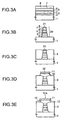
- FIG. 3A on an n type (100) InP substrate 1, an n type InP Buffer layer 2 having carrier concentration of 1X10 18 cm -3 and thickness of 0.8 ⁇ m, an n type InGaAsP optical guide layer 3 having band gap wavelength of 1.13 ⁇ m, an n type InP clad layer 4 having carrier concentration of 5x10 17 cm -3 and thickness of 0.5 ⁇ m, an MQW optical absorption layer 5 composed of alternately laminated nine InGaAsP well layers each 7nm thick and having band gap wavelength of 1.55 ⁇ m and 10 ten InGaAsP barrier layers each 5.2nm thick and having band gap wavelength of 1.2 ⁇ m, a p type InGaAsP clad layer 6 having carrier concentration of 5 ⁇ 10 17 cm -3 , band gap wavelength of 1.05 ⁇ m and thickness of 0.5 ⁇ m, a p - type InP impurity diffusion
- a SiO 2 film is deposited on a whole surface of the p type InP clad layer 8 by thermal CVD and a SiO 2 mask 21 having a striped pattern 1.5 ⁇ m wide is formed by using usual photolithography.
- the multi-layered structure is etched up to the n type InP substrate 1 by reactive ion beam etching (RIBE) method to form a waveguide 20 having a striped multi-layered structure.
- RIBE reactive ion beam etching
- the etching of the multi-layered structure may be made up to a middle of the buffer layer 2.
- the striped waveguide 20 is buried by semi-insulating InP burying layers 9 having thickness as large as a height of the striped waveguide 20 and formed on both sides of the striped waveguide 20 by MOVPE while the SiO 2 mask 21 on an upper portion of the waveguide 20 being left as it is.
- the SiO 2 mask 21 on an upper portion of the waveguide 20 is removed and, then, a p + type InP clad layer 10 having carrier concentration of 1 ⁇ 10 18 cm -3 and thickness of 1 ⁇ m and a p + type InGaAs contact layer 11 having carrier concentration of 1 ⁇ 10 19 cm -3 and thickness of 0.2 ⁇ m are grown on whole surfaces of the InP clad layer 8 and the semi-insulating InP burying layer 9 by MOVPE.
- a striped SiO 2 mask 22 is formed by photolithography and, then, the p + type InGaAs contact layer 11 and the p + type InP clad layer 10 are removed by chemical etching to form a striped p + type InP clad layer 10 and p + type InGaAs contact layer 11 immediately above the waveguide.
- a SiO 2 protective layer 12 is deposited on a whole surface of the wafer by thermal CVD. Then, a portion of the SiO 2 protective layer 12, which includes the immediate above portion of the waveguide, is removed by usual photolithography to form a striped opening 12a in the SiO 2 protective layer 12.
- an electrode pattern is formed by using usual photolithography.
- the InP substrate 1 is polished up to an appropriate thickness and the electroabsorption type optical modulator shown in FIG. 2 is completed by forming an electrode 14 on a rear surface of the InP substrate 1.
- Opposite edge faces of the optical modulator thus fabricated were coated with films each having reflectivity of 0.1% and the characteristics thereof was evaluated.
- the extinction characteristics of the optical modulator measured by inputting a laser light from a distributed feedback (DFB) laser having oscillation wavelength of 1.550 ⁇ m thereto is shown by a curve 51 in FIG. 5.
- the non-linearity of the extinction characteristics is improved.
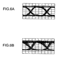
- the non-return-to-zero (NRZ) modulation waveform at 10Gb/s was measured.
- a result is shown in FIG. 6A. As is clear from FIG. 6A, it is clear that the cross point position is improved.
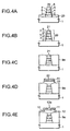
- FIGS. 4A to 4E A second embodiment of the fabrication method of the present optical modulator is shown in FIGS. 4A to 4E. The second embodiment will be described with reference to FIGS. 2 and 4A to 4E.
- a SiO 2 film 100nm thick is deposited on an n type (100) InP substrate 1 by thermal CVD and a SiO 2 mask 23 is formed by patterning the SiO 2 film such that a striped opening extends in [011] direction of the InP substrate. Width of the opening of the mask 23 was 1.5 ⁇ m in this case.
- an n type InP buffer layer 2 having carrier concentration of 1 ⁇ 10 19 cm -3 and thickness of 0.8 ⁇ m
- an n type InGaAsP optical guide layer 3 having band gap wavelength of 1.13 ⁇ m
- an n type InP clad layer 4 having carrier concentration of 5 ⁇ 10 17 cm -3 and thickness of 0.5 ⁇ m
- an MQW optical absorption layer 5 composed of alternately laminated nine InGaAsP well layers each 7nm thick and having band gap wavelength of 1.55 ⁇ m and ten InGaAsP barrier layers each 5.2nm thick and having band gap wavelength of 1.2 ⁇ m
- a p type InGaAsP clad layer 6 having carrier concentration of 5 ⁇ 10 17 cm -3 , band gap wavelength of 1.05 ⁇ m and thickness of 0.5 ⁇ m
- a p - type InP impurity diffusion inhibiting layer 7 having carrier concentration of 2 ⁇ 10 17 cm -3 and thickness of 0.1 ⁇ m
- a p type InP clad layer 8 having carrier concentration of 5 ⁇
- a SiO 2 mask 21 is formed on only the waveguide by thermal CVD and photolithography after the SiO 2 mask 23 is removed.
- the striped waveguide 20 is buried by Fe doped high resistance burying layers 9a having thickness substantially the same as height of the striped waveguide 20 grown on both sides of the striped waveguide 20 by MOVPE with using the SiO 2 mask 21 as a selective growing mask.
- the SiO 2 mask 21 on the waveguide 20 is removed and, then, a p + type InP clad layer 10 having carrier concentration of 1 ⁇ 10 18 cm -3 and thickness of 1 ⁇ m and a p + type InGaAs contact layer 11 having carrier concentration of 1 ⁇ 10 19 cm -3 and thickness of 0.2 ⁇ m are grown on whole surfaces of the InP clad layer 8 and the high resistance InP burying layers 9a by MOVPE.
- a striped SiO 2 mask 22 is formed by photolithography and, then, the p + type InGaAs contact layer 11 and the p + type InP clad layer 10 are removed by chemical etching to making the p + type InP clad layer 10 and the p+ type InGaAs contact layer 11 immediately above the waveguide as striped.
- a SiO 2 protective layer 12 is deposited on a whole surface of the wafer by thermal CVD. Then, a portion of the SiO 2 protective layer 12, which includes the immediate above portion of the waveguide, is removed by usual photolithography to form a striped opening 12a in the SiO 2 protective layer 12.
- an electrode pattern is formed by using usual photolithography.
- the InP substrate 1 is polished up to an appropriate depth and the electroabsorption type optical modulator shown in FIG. 2 is completed by forming an electrode 14 on a rear surface of the InP substrate 1.
- the buffer layer 2 is formed on the substrate, the buffer layer 2 may be omitted. Furthermore, the optical guide layer 3 may be also omitted. Moreover, although the burying layers 9 (9a) are selectively grown after the striped waveguide 20 having the multi-layered structure is formed, it may be possible that, after a burying layer is formed on the substrate, a groove is formed in the burying layer by etching and, then, the waveguide is formed in the groove by selective growing. In the latter case, the impurity diffusion preventing effect may be superior than those obtained by the described embodiments since the number of the heating steps (crystal growing steps) after the formation of the waveguide is smaller than that of any of the described embodiments by one.
- the impurity diffusion inhibiting layer 7 of p - type InP having low carrier concentration is provided between the p type InGaAsP clad layer 6 and the p type InP clad layer 8 on the MQW optical absorption layer. Furthermore, the diffusion speed of Zn is highest in InGaAs, and lowest in InP, that in InGaAsP being in between.
- the modulation waveform is improved in cross point position as shown in FIG. 6A. Furthermore, the improvement of the cross point position corresponds to shorting of the rising time tr and the falling time tf of the optical signal waveform. Therefore, the modulation speed of the optical modulator is improved.
Landscapes
- Physics & Mathematics (AREA)
- Chemical & Material Sciences (AREA)
- Optics & Photonics (AREA)
- Nonlinear Science (AREA)
- Engineering & Computer Science (AREA)
- Nanotechnology (AREA)
- General Physics & Mathematics (AREA)
- Life Sciences & Earth Sciences (AREA)
- Biophysics (AREA)
- Crystallography & Structural Chemistry (AREA)
- Optical Modulation, Optical Deflection, Nonlinear Optics, Optical Demodulation, Optical Logic Elements (AREA)
- Semiconductor Lasers (AREA)
- Optical Integrated Circuits (AREA)
Description
Claims (4)
- A semiconductor electroabsorption type optical modulator comprising:characterized in that each of said first upper cladding layer (6) and said impurity diffusion inhibiting layer (7) is doped with impurities to represent the second conductivity type, and that said impurity diffusion inhibiting layer (7) has a dopant impurity atom concentration lower than that of said first upper cladding layer (6).a stripe waveguide (20) having a multi-layer structure which comprises an optical guide layer (3) of a first conductivity type, a lower cladding layer (4) of the first conductivity type provided on said optical guide layer (3) and having a band gap larger than that of an optical absorption layer, said optical absorption layer (5) provided on said lower cladding layer (4), a first upper cladding layer (6) provided on said optical absorption layer (5) and having a band gap larger than that of said optical absorption layer, an impurity diffusion inhibiting layer (7) provided on said first upper cladding layer (6), and a second upper cladding layer (8) of a second conductivity type provided on said impurity diffusion inhibiting layer (7), wherein the first and second conductivity types are different from each other,and a third upper cladding layer (10) of the second conductivity type provided on said second upper cladding layer (8);
- A semiconductor electroabsorption type optical modulator as claimed in claim 1, wherein said impurity diffusion inhibiting layer (7) is made of a compound semiconductor other than the compound semiconductor which constructs said first upper cladding layer (6), wherein the diffusion velocity of the impurity particle in said impurity diffusion inhibiting layer (7) is smaller than the one of said first upper cladding layer (6).
- A semiconductor electroabsorption type optical modulator as claimed in claim 1, further comprising a semi-insulating burying layer (9) disposed along the two sides of said stripe waveguide (20) which are substantially perpendicular to the plane of the optical guiding layer.
- A semiconductor electroabsorption type optical modulator as claimed in claim 3, wherein said lower cladding layer (4), said impurity diffusion inhibiting layer (7), and said second upper cladding layer (8) are formed of InP, said optical guide layer (3) is formed of InGaAsP, said optical absorption layer (5) is formed of InGaAsP Multiple Quantum Well material and said first upper cladding layer (6) is formed of InGaAsP.
Applications Claiming Priority (2)
| Application Number | Priority Date | Filing Date | Title |
|---|---|---|---|
| JP19800899 | 1999-07-12 | ||
| JP19800899A JP3384447B2 (en) | 1999-07-12 | 1999-07-12 | Absorption type optical modulator and method of manufacturing the same |
Publications (3)
| Publication Number | Publication Date |
|---|---|
| EP1069456A2 EP1069456A2 (en) | 2001-01-17 |
| EP1069456A3 EP1069456A3 (en) | 2003-03-05 |
| EP1069456B1 true EP1069456B1 (en) | 2005-04-13 |
Family
ID=16383985
Family Applications (1)
| Application Number | Title | Priority Date | Filing Date |
|---|---|---|---|
| EP00115143A Expired - Lifetime EP1069456B1 (en) | 1999-07-12 | 2000-07-12 | Electroabsorption optical modulator and fabrication method thereof |
Country Status (4)
| Country | Link |
|---|---|
| US (1) | US6477283B1 (en) |
| EP (1) | EP1069456B1 (en) |
| JP (1) | JP3384447B2 (en) |
| DE (1) | DE60019375T2 (en) |
Families Citing this family (10)
| Publication number | Priority date | Publication date | Assignee | Title |
|---|---|---|---|---|
| DE10135958B4 (en) | 2001-07-24 | 2008-05-08 | Finisar Corp., Sunnyvale | Electroabsorption modulator, modulator laser device, and method of making an electroabsorption modulator |
| US6665105B2 (en) * | 2001-07-31 | 2003-12-16 | Agility Communications, Inc. | Tunable electro-absorption modulator |
| US7058246B2 (en) | 2001-10-09 | 2006-06-06 | Infinera Corporation | Transmitter photonic integrated circuit (TxPIC) chip with enhanced power and yield without on-chip amplification |
| JP2003241152A (en) * | 2002-02-18 | 2003-08-27 | Mitsubishi Electric Corp | Semiconductor optical modulator |
| US20050141800A1 (en) * | 2002-09-17 | 2005-06-30 | Mitsubishi Denki Kabushiki Kaisha | Waveguide semiconductor optical device and process of fabricating the device |
| US7037739B2 (en) * | 2004-01-06 | 2006-05-02 | Korea Institute Of Science And Technology | Fabrication method of an epilayer structure InGaAsP/InP ridge waveguide phase modulator with high phase modulation efficiency |
| US8034648B1 (en) * | 2006-05-15 | 2011-10-11 | Finisar Corporation | Epitaxial regrowth in a distributed feedback laser |
| JP5463760B2 (en) * | 2009-07-02 | 2014-04-09 | 三菱電機株式会社 | Optical waveguide integrated semiconductor optical device and manufacturing method thereof |
| JP6291849B2 (en) * | 2014-01-10 | 2018-03-14 | 三菱電機株式会社 | Semiconductor device manufacturing method, semiconductor device |
| JP6414306B2 (en) * | 2017-09-27 | 2018-10-31 | 三菱電機株式会社 | Semiconductor device manufacturing method, semiconductor device |
Family Cites Families (11)
| Publication number | Priority date | Publication date | Assignee | Title |
|---|---|---|---|---|
| US4802182A (en) * | 1987-11-05 | 1989-01-31 | Xerox Corporation | Monolithic two dimensional waveguide coupled cavity laser/modulator |
| US5112761A (en) * | 1990-01-10 | 1992-05-12 | Microunity Systems Engineering | Bicmos process utilizing planarization technique |
| US5171713A (en) * | 1990-01-10 | 1992-12-15 | Micrunity Systems Eng | Process for forming planarized, air-bridge interconnects on a semiconductor substrate |
| US5182225A (en) * | 1990-01-10 | 1993-01-26 | Microunity Systems Engineering, Inc. | Process for fabricating BICMOS with hypershallow junctions |
| JPH06222406A (en) | 1993-01-26 | 1994-08-12 | Nippon Telegr & Teleph Corp <Ntt> | Semiconductor optical device |
| JP3234086B2 (en) * | 1994-01-18 | 2001-12-04 | キヤノン株式会社 | Optical semiconductor device and method for manufacturing the same |
| US5889913A (en) * | 1995-03-15 | 1999-03-30 | Kabushiki Kaisha Toshiba | Optical semiconductor device and method of fabricating the same |
| DE19624514C1 (en) * | 1996-06-19 | 1997-07-17 | Siemens Ag | Monolithically integrated semiconductor laser-modulator combination |
| JPH1090635A (en) | 1996-09-13 | 1998-04-10 | Nippon Telegr & Teleph Corp <Ntt> | Embedded semiconductor optical device |
| GB2323450A (en) * | 1997-03-20 | 1998-09-23 | Secr Defence | Optical modulator |
| US6088500A (en) * | 1997-04-11 | 2000-07-11 | Trw Inc. | Expanded mode wave guide semiconductor modulation |
-
1999
- 1999-07-12 JP JP19800899A patent/JP3384447B2/en not_active Expired - Fee Related
-
2000
- 2000-07-07 US US09/611,902 patent/US6477283B1/en not_active Expired - Fee Related
- 2000-07-12 DE DE60019375T patent/DE60019375T2/en not_active Expired - Fee Related
- 2000-07-12 EP EP00115143A patent/EP1069456B1/en not_active Expired - Lifetime
Also Published As
| Publication number | Publication date |
|---|---|
| DE60019375T2 (en) | 2005-09-08 |
| EP1069456A2 (en) | 2001-01-17 |
| EP1069456A3 (en) | 2003-03-05 |
| JP2001021851A (en) | 2001-01-26 |
| DE60019375D1 (en) | 2005-05-19 |
| US6477283B1 (en) | 2002-11-05 |
| JP3384447B2 (en) | 2003-03-10 |
Similar Documents
| Publication | Publication Date | Title |
|---|---|---|
| JP2762951B2 (en) | Semiconductor optical waveguide and manufacturing method thereof | |
| US5459747A (en) | Semiconductor optical devices | |
| JP2842292B2 (en) | Semiconductor optical integrated device and manufacturing method | |
| JPH1075009A (en) | Optical semiconductor device and its manufacture | |
| JP2967737B2 (en) | Optical semiconductor device and its manufacturing method | |
| US6100543A (en) | Electro-absorption type semiconductor optical modulator having a quantum well structure | |
| EP0378098B1 (en) | Semiconductor optical device | |
| CN1272885C (en) | Distributed feedback semiconductor laser and electric absorption modulator integrated light source and mfg. method | |
| JP2937751B2 (en) | Method for manufacturing optical semiconductor device | |
| US6477283B1 (en) | Electroabsorption optical modulator and fabrication method thereof | |
| EP0661783B1 (en) | Method for fabricating semiconductor light integrated circuit | |
| JP4690515B2 (en) | Optical modulator, semiconductor optical device, and manufacturing method thereof | |
| US5519721A (en) | Multi-quantum well (MQW) structure laser diode/modulator integrated light source | |
| JP2021028971A (en) | Embedded semiconductor optical element | |
| KR100305301B1 (en) | Method of manufacturing optical semiconductor device | |
| JPH0750815B2 (en) | Method for manufacturing semiconductor optical integrated device | |
| US6602432B2 (en) | Electroabsorption modulator, and fabricating method of the same | |
| JPH08234148A (en) | Optical semiconductor device and its production | |
| JPH077232A (en) | Optical semiconductor device | |
| JP3146821B2 (en) | Manufacturing method of semiconductor optical integrated device | |
| GB2292011A (en) | Semiconductor optical devices and methods for fabrication | |
| JPH08292336A (en) | Production of optical semiconductor integrated circuit | |
| JP3159914B2 (en) | Selectively grown waveguide type optical control element and method of manufacturing the same | |
| JP2760276B2 (en) | Selectively grown waveguide type optical control device | |
| JP2842387B2 (en) | Manufacturing method of semiconductor optical integrated device |
Legal Events
| Date | Code | Title | Description |
|---|---|---|---|
| PUAI | Public reference made under article 153(3) epc to a published international application that has entered the european phase |
Free format text: ORIGINAL CODE: 0009012 |
|
| AK | Designated contracting states |
Kind code of ref document: A2 Designated state(s): AT BE CH CY DE DK ES FI FR GB GR IE IT LI LU MC NL PT SE |
|
| AX | Request for extension of the european patent |
Free format text: AL;LT;LV;MK;RO;SI |
|
| PUAL | Search report despatched |
Free format text: ORIGINAL CODE: 0009013 |
|
| RAP1 | Party data changed (applicant data changed or rights of an application transferred) |
Owner name: NEC COMPOUND SEMICONDUCTOR DEVICES, LTD. |
|
| AK | Designated contracting states |
Kind code of ref document: A3 Designated state(s): AT BE CH CY DE DK ES FI FR GB GR IE IT LI LU MC NL PT SE |
|
| AX | Request for extension of the european patent |
Extension state: AL LT LV MK RO SI |
|
| 17P | Request for examination filed |
Effective date: 20030124 |
|
| 17Q | First examination report despatched |
Effective date: 20030508 |
|
| AKX | Designation fees paid |
Designated state(s): DE FR GB IT NL |
|
| GRAP | Despatch of communication of intention to grant a patent |
Free format text: ORIGINAL CODE: EPIDOSNIGR1 |
|
| GRAS | Grant fee paid |
Free format text: ORIGINAL CODE: EPIDOSNIGR3 |
|
| GRAA | (expected) grant |
Free format text: ORIGINAL CODE: 0009210 |
|
| AK | Designated contracting states |
Kind code of ref document: B1 Designated state(s): DE FR GB IT NL |
|
| PG25 | Lapsed in a contracting state [announced via postgrant information from national office to epo] |
Ref country code: NL Free format text: LAPSE BECAUSE OF FAILURE TO SUBMIT A TRANSLATION OF THE DESCRIPTION OR TO PAY THE FEE WITHIN THE PRESCRIBED TIME-LIMIT Effective date: 20050413 |
|
| REG | Reference to a national code |
Ref country code: GB Ref legal event code: FG4D |
|
| REG | Reference to a national code |
Ref country code: IE Ref legal event code: FG4D |
|
| REF | Corresponds to: |
Ref document number: 60019375 Country of ref document: DE Date of ref document: 20050519 Kind code of ref document: P |
|
| NLV1 | Nl: lapsed or annulled due to failure to fulfill the requirements of art. 29p and 29m of the patents act | ||
| PLBE | No opposition filed within time limit |
Free format text: ORIGINAL CODE: 0009261 |
|
| STAA | Information on the status of an ep patent application or granted ep patent |
Free format text: STATUS: NO OPPOSITION FILED WITHIN TIME LIMIT |
|
| ET | Fr: translation filed | ||
| 26N | No opposition filed |
Effective date: 20060116 |
|
| REG | Reference to a national code |
Ref country code: GB Ref legal event code: 732E |
|
| REG | Reference to a national code |
Ref country code: FR Ref legal event code: TP |
|
| PGFP | Annual fee paid to national office [announced via postgrant information from national office to epo] |
Ref country code: FR Payment date: 20090710 Year of fee payment: 10 |
|
| PGFP | Annual fee paid to national office [announced via postgrant information from national office to epo] |
Ref country code: GB Payment date: 20090708 Year of fee payment: 10 Ref country code: DE Payment date: 20090709 Year of fee payment: 10 |
|
| PGFP | Annual fee paid to national office [announced via postgrant information from national office to epo] |
Ref country code: IT Payment date: 20090722 Year of fee payment: 10 |
|
| GBPC | Gb: european patent ceased through non-payment of renewal fee |
Effective date: 20100712 |
|
| REG | Reference to a national code |
Ref country code: FR Ref legal event code: ST Effective date: 20110331 |
|
| PG25 | Lapsed in a contracting state [announced via postgrant information from national office to epo] |
Ref country code: DE Free format text: LAPSE BECAUSE OF NON-PAYMENT OF DUE FEES Effective date: 20110201 |
|
| REG | Reference to a national code |
Ref country code: DE Ref legal event code: R119 Ref document number: 60019375 Country of ref document: DE Effective date: 20110201 |
|
| PG25 | Lapsed in a contracting state [announced via postgrant information from national office to epo] |
Ref country code: IT Free format text: LAPSE BECAUSE OF NON-PAYMENT OF DUE FEES Effective date: 20100712 Ref country code: FR Free format text: LAPSE BECAUSE OF NON-PAYMENT OF DUE FEES Effective date: 20100802 |
|
| PG25 | Lapsed in a contracting state [announced via postgrant information from national office to epo] |
Ref country code: GB Free format text: LAPSE BECAUSE OF NON-PAYMENT OF DUE FEES Effective date: 20100712 |