EP1065916A2 - Resin sealed electronic device - Google Patents
Resin sealed electronic device Download PDFInfo
- Publication number
- EP1065916A2 EP1065916A2 EP00113077A EP00113077A EP1065916A2 EP 1065916 A2 EP1065916 A2 EP 1065916A2 EP 00113077 A EP00113077 A EP 00113077A EP 00113077 A EP00113077 A EP 00113077A EP 1065916 A2 EP1065916 A2 EP 1065916A2
- Authority
- EP
- European Patent Office
- Prior art keywords
- resin
- heat sink
- electronic device
- power element
- sealed electronic
- Prior art date
- Legal status (The legal status is an assumption and is not a legal conclusion. Google has not performed a legal analysis and makes no representation as to the accuracy of the status listed.)
- Granted
Links
Images




Classifications
-
- H—ELECTRICITY
- H05—ELECTRIC TECHNIQUES NOT OTHERWISE PROVIDED FOR
- H05K—PRINTED CIRCUITS; CASINGS OR CONSTRUCTIONAL DETAILS OF ELECTRIC APPARATUS; MANUFACTURE OF ASSEMBLAGES OF ELECTRICAL COMPONENTS
- H05K5/00—Casings, cabinets or drawers for electric apparatus
- H05K5/06—Hermetically-sealed casings
- H05K5/065—Hermetically-sealed casings sealed by encapsulation, e.g. waterproof resin forming an integral casing, injection moulding
-
- F—MECHANICAL ENGINEERING; LIGHTING; HEATING; WEAPONS; BLASTING
- F02—COMBUSTION ENGINES; HOT-GAS OR COMBUSTION-PRODUCT ENGINE PLANTS
- F02P—IGNITION, OTHER THAN COMPRESSION IGNITION, FOR INTERNAL-COMBUSTION ENGINES; TESTING OF IGNITION TIMING IN COMPRESSION-IGNITION ENGINES
- F02P3/00—Other installations
- F02P3/02—Other installations having inductive energy storage, e.g. arrangements of induction coils
-
- H—ELECTRICITY
- H10—SEMICONDUCTOR DEVICES; ELECTRIC SOLID-STATE DEVICES NOT OTHERWISE PROVIDED FOR
- H10W—GENERIC PACKAGES, INTERCONNECTIONS, CONNECTORS OR OTHER CONSTRUCTIONAL DETAILS OF DEVICES COVERED BY CLASS H10
- H10W40/00—Arrangements for thermal protection or thermal control
- H10W40/70—Fillings or auxiliary members in containers or in encapsulations for thermal protection or control
- H10W40/77—Auxiliary members characterised by their shape
- H10W40/778—Auxiliary members characterised by their shape in encapsulations
-
- H—ELECTRICITY
- H10—SEMICONDUCTOR DEVICES; ELECTRIC SOLID-STATE DEVICES NOT OTHERWISE PROVIDED FOR
- H10W—GENERIC PACKAGES, INTERCONNECTIONS, CONNECTORS OR OTHER CONSTRUCTIONAL DETAILS OF DEVICES COVERED BY CLASS H10
- H10W74/00—Encapsulations, e.g. protective coatings
- H10W74/10—Encapsulations, e.g. protective coatings characterised by their shape or disposition
- H10W74/131—Encapsulations, e.g. protective coatings characterised by their shape or disposition the semiconductor body being only partially enclosed
-
- H—ELECTRICITY
- H05—ELECTRIC TECHNIQUES NOT OTHERWISE PROVIDED FOR
- H05K—PRINTED CIRCUITS; CASINGS OR CONSTRUCTIONAL DETAILS OF ELECTRIC APPARATUS; MANUFACTURE OF ASSEMBLAGES OF ELECTRICAL COMPONENTS
- H05K3/00—Apparatus or processes for manufacturing printed circuits
- H05K3/22—Secondary treatment of printed circuits
- H05K3/28—Applying non-metallic protective coatings
- H05K3/284—Applying non-metallic protective coatings for encapsulating mounted components
-
- H—ELECTRICITY
- H10—SEMICONDUCTOR DEVICES; ELECTRIC SOLID-STATE DEVICES NOT OTHERWISE PROVIDED FOR
- H10W—GENERIC PACKAGES, INTERCONNECTIONS, CONNECTORS OR OTHER CONSTRUCTIONAL DETAILS OF DEVICES COVERED BY CLASS H10
- H10W72/00—Interconnections or connectors in packages
- H10W72/50—Bond wires
- H10W72/531—Shapes of wire connectors
- H10W72/5363—Shapes of wire connectors the connected ends being wedge-shaped
-
- H—ELECTRICITY
- H10—SEMICONDUCTOR DEVICES; ELECTRIC SOLID-STATE DEVICES NOT OTHERWISE PROVIDED FOR
- H10W—GENERIC PACKAGES, INTERCONNECTIONS, CONNECTORS OR OTHER CONSTRUCTIONAL DETAILS OF DEVICES COVERED BY CLASS H10
- H10W72/00—Interconnections or connectors in packages
- H10W72/50—Bond wires
- H10W72/551—Materials of bond wires
- H10W72/552—Materials of bond wires comprising metals or metalloids, e.g. silver
- H10W72/5524—Materials of bond wires comprising metals or metalloids, e.g. silver comprising aluminium [Al]
-
- H—ELECTRICITY
- H10—SEMICONDUCTOR DEVICES; ELECTRIC SOLID-STATE DEVICES NOT OTHERWISE PROVIDED FOR
- H10W—GENERIC PACKAGES, INTERCONNECTIONS, CONNECTORS OR OTHER CONSTRUCTIONAL DETAILS OF DEVICES COVERED BY CLASS H10
- H10W74/00—Encapsulations, e.g. protective coatings
Definitions
- the present invention relates to a structure of a resin sealed electronic device and, more particularly to a package structure and configuration to improve its reliability.
- Japanese Patent No. 2,590,601 proposes to seal a circuit board and a semiconductor element with transfer mold. Further, Japanese Patent Application Laid-Open No. 9-177647 discloses an igniter which is formed in one chip by constructing a function circuit on a semiconductor chip.
- a metallic heat sink in order to mount a semiconductor element, has nickel plating on its mounting surface or additionally has silver plating or the like on the nickel plating.
- plating methods There are two plating methods, that is, one is that the heat sink is plated after being pressed into a part-mounting shape, and the other is that the heat sink is plated before being pressed.
- These kinds of plating are poor in adhesion to the resin, and consequently weak in a force restraining the heat sink portion.
- the heat sink is plated when it is in its material state, and the reverse side surface of the surface mounting the parts is masked so as to be not plated.
- the base material surface of the metallic material (a cooper group or an aluminum group material) is tighter in adhesion to the resin compared to that of the plating described above, and consequently the thermal displacement can be restrained.
- the semiconductor parts and the board are actually mounted on the surface of mounting the parts, and the exposed plated area having a weak adhering force is small. Therefore, tightness of adhesion of the semiconductor power element to the resin is maintained by coating the surface of the element, and tightness of adhesion of the reverse side surface to the transfer mold resin is improved by the base material surface of the metallic material without the plating. By doing so, the thermal displacement of the portion of the semiconductor power element is reduced by restraining the upper and the lower surfaces.
- the portion of the hybrid IC the difference of the linear expansion coefficients between the substrate material of the aluminum group ceramic and the metallic heat sink material (the copper group or the aluminum group material) is small compared to the difference in the portion of the power element. Therefore, the reliability can be improved by improving the tightness of adhesion of the reverse side surface of the heat sink to the resin to restrain the displacement in the heat sink side.
- the thermal stresses acting on the contained parts can be reduced by using a mold resin having a linear expansion coefficient within a range of the smallest linear expansion coefficient (3 ⁇ 10 -6 /°C) of silicon in the semiconductor element among the constituent materials of the contained parts to the linear expansion coefficient (17 ⁇ 10 -6 /°C) of copper among the metallic materials (the copper group or the aluminum group material) to be used for the heat sink which has the largest volume.
- FIG. 1 is a cross-sectional side view showing an embodiment of a resin sealed electronic device in accordance with the present invention.
- An input/output terminal portion 6 is connected to a circuit board through aluminum wires 5 and wire bonding pads 8. Print resistors, capacitors, MIC and so on are formed on the circuit board 4. A signal output from the circuit board 4 through an aluminum wire 5 drives a power element 1.
- the circuit board 4 is fixed on a metallic heat sink 3 with an adhesive.
- FIG. 2 is a perspective view showing a chip portion of the semiconductor power element.
- the upper surface (surface to be in contact with the resin) except for portions 1b to be used for the bonding pad portions of the semiconductor power element 1 is coated with a polyimide group resin or a polyamide group resin at manufacturing the element (portion 1a).
- FIG. 3 is a perspective view showing an embodiment of a resin sealed electronic device in accordance with the present invention.
- the exterior of the mold resin portion 7 in the figure is illustrated only its outward form so as to easily understood the internal structure. Therein, the parts are identified by the same reference characters as in FIG. 1, and detailed explanation will be omitted here.
- the thermal stress is reduced by using a mold resin having a linear expansion coefficient within a range of the smallest linear expansion coefficient of 3 ⁇ 10 -6 /°C of the power element 1 to the linear expansion coefficient of 17 ⁇ 10 -6 /°C of copper among the metallic materials (the copper group or the aluminum group material) of the heat sink for the mold resin 7.
- FIG. 4 is a perspective view showing an embodiment of a heat sink portion in accordance with the present invention seeing from the reverse side.
- Depressing portions 3b are formed on the reverse side surface 3a of the heat sink 3. By doing so, an area in contact with the resin is increased to improve the tightness of adhesion to the resin.
- the depressing portions in this example are line-shaped projections aligned in rows spaced an equal interval, the same effect can be attained by projections of any shapes such as prism, cone, semi-sphere and the like as far as the projections are capable of expanding the contact area.
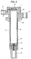
- FIG. 5 shows an example in a case where a resin sealed electronic device in accordance with the present invention is mounted on an ignition coil for a vehicle.
- the figure of this embodiment shows the ignition coil for a vehicle in which the circuit configuration in the resin sealed electronic device in accordance with the present invention is formed in an igniter circuit for ignition (Although this embodiment will be described that a cylindrical coil is used, the present invention is not limited to the shape of the coil).
- a case 23 of a cylindrical coil 31 contains a primary and a secondary coils 30 (not shown in detail) and the resin sealed electronic device 20 in accordance with the present invention, and is filled with an injection type epoxy resin 24 to embed them.
- the signal and the electric power to the coil are input through terminals 22 in a connector portion 21.
- the secondary voltage generated by the coil is supplied to a spark plug (not shown) through a spring 28 attached to a high voltage terminal 27.
- a boot portion 29 is engaged with the spark plug 29 to make the connection portion waterproof.
- a plug hole seal 26 is engaged with a plug hole when the cylindrical coil is mounted onto the engine to make the connection portion waterproof.
- the coil is fixed to the engine by the bush portion 25 attached to the coil case using a bolt.
- the transfer mold resin can increase the restraint force between the power element (for example, insulated gate bipolar transistor) and the lead frame of the main internal components, and the reliability can be maintained even if the outside of the present electronic device is further embedded with the resin having a different linear expansion coefficient.
- the power element for example, insulated gate bipolar transistor
- FIG. 6 is a circuit diagram of the coil of FIG. 5.
- Electric power is supplied from an electric power source 33 to the coil 31 containing the resin sealed electronic device having the circuit configuration of the igniter.
- a hybrid circuit 30b mounting a flip chip and the power element portion 30a (in this case, an insulated gate bipolar transistor) are contained in the resin sealed electronic device having the circuit configuration of the igniter.
- a signal from an engine control unit (not shown) is signal processed by the hybrid circuit 30 b , and then drives the power element 30 a to conduct and interrupt the primary current of the coil 30. At that time, a high voltage is generated in the secondary side of the coil 30 to be supplied to the spark plug 32.
- FIG. 7 is a chart showing operating waveforms of the coil of FIG. 6.
- the secondary voltage V2 is generated in the secondary side of the coil. It is not shown in the figure that the primary current is generally interrupted at approximately 6 to 8 A, and at that time the generated secondary voltage is approximately 20 to 30 kV.
- FIG. 8 is a view showing a feature of the coils mounted on an engine.
- the embodiment is the cylindrical coil
- the coils are inserted into and attached to the plug holes of the engine.
- the present resin sealed electronic device is incorporated in the coil as described above, because the coil is directly attached to the engine, it is particularly necessary to take the thermal stress into consideration. However, it is possible to maintain the reliability by applying the present invention.
- a power element coated with a polyimide group or a polyamide group resin at manufacturing the element is used for the power element to moderate the stress acting on the power element portion by improving the tightness of adhesion to the mold resin. Further, by using the heat sink having the non-plated portions (portions being left the base material of the heat sink as it is) where the board and the semiconductor power element are mounted, tightness of adhesion of the heat sink to the mold resin is increased.
- the thermal stress acting on the contained components can be reduced, and the thermal cycle resistance can be improved, and accordingly the high reliability can be attained.
Landscapes
- Engineering & Computer Science (AREA)
- Microelectronics & Electronic Packaging (AREA)
- Chemical & Material Sciences (AREA)
- Combustion & Propulsion (AREA)
- Mechanical Engineering (AREA)
- General Engineering & Computer Science (AREA)
- Ignition Installations For Internal Combustion Engines (AREA)
- Structures Or Materials For Encapsulating Or Coating Semiconductor Devices Or Solid State Devices (AREA)
- Cooling Or The Like Of Semiconductors Or Solid State Devices (AREA)
Abstract
Description
Claims (5)
- A resin sealed electronic device which is formed by fixing a hybrid IC board (4) composing an electronic circuit; a semiconductor power element (1) operated by a signal from said electronic circuit; a heat sink (3) mounting said board (4) and said semiconductor element (1), said heat sink (3) being made of a metallic material; and input and output terminals (6) with transfer mold by a resin (7), wherein a surface (1a) of the semiconductor power element (1) opposite to a surface facing said heat sink (3) is coated with a polyimide group or a polyamide group material, and the reverse side surface (3a) of the heat sink (3) bares a metallic base material of the heat sink (3), and a linear expansion coefficient of said resin (7) is within a range of 3x10⁻⁶/°C to 17x10-6/°C.
- A resin sealed electronic device according to claim 1, wherein the material of said heat sink (3) is a copper group material.
- A resin sealed electronic device according to claim 1, wherein the material of said heat sink (3) is an aluminum group material.
- A resin sealed electronic device according to any one of claim 1 to claim 3, wherein projections and depressions (3b) are formed on the reverse side surface (3a) of the heat sink portion (3) of the metallic base to further improve tightness of adhesion to the resin.
- A resin sealed electronic device according to any one of claim 1 to claim 4, wherein an ignition coil containing type igniter for a vehicle is constructed by forming a control circuit for controlling conducting and interrupting of a primary current of the igniter according to an ignition signal from an engine control unit in the electronic circuit portion on the hybrid IC board, and by using a bipolar power transistor or an insulated gate bipolar power transistor for conducting and interrupting the primary current for the semiconductor power element.
Applications Claiming Priority (2)
| Application Number | Priority Date | Filing Date | Title |
|---|---|---|---|
| JP18107199 | 1999-06-28 | ||
| JP18107199A JP3866880B2 (en) | 1999-06-28 | 1999-06-28 | Resin-sealed electronic device |
Publications (3)
| Publication Number | Publication Date |
|---|---|
| EP1065916A2 true EP1065916A2 (en) | 2001-01-03 |
| EP1065916A3 EP1065916A3 (en) | 2001-10-04 |
| EP1065916B1 EP1065916B1 (en) | 2006-08-16 |
Family
ID=16094303
Family Applications (1)
| Application Number | Title | Priority Date | Filing Date |
|---|---|---|---|
| EP00113077A Expired - Lifetime EP1065916B1 (en) | 1999-06-28 | 2000-06-26 | Resin sealed electronic device |
Country Status (4)
| Country | Link |
|---|---|
| US (1) | US6484708B2 (en) |
| EP (1) | EP1065916B1 (en) |
| JP (1) | JP3866880B2 (en) |
| DE (1) | DE60030045T2 (en) |
Cited By (5)
| Publication number | Priority date | Publication date | Assignee | Title |
|---|---|---|---|---|
| EP1388667A1 (en) * | 2002-08-06 | 2004-02-11 | Delphi Technologies, Inc. | Ignition coil driver chip on printed circuit board for plughole coil housing |
| US6903457B2 (en) * | 2002-11-13 | 2005-06-07 | Mitsubishi Denki Kabushiki Kaisha | Power semiconductor device |
| WO2008080533A1 (en) * | 2006-12-29 | 2008-07-10 | Nokia Corporation | An electronic device and method of assembling an electronic device |
| WO2012072312A1 (en) * | 2010-12-02 | 2012-06-07 | Robert Bosch Gmbh | Ignition coil having integrated electronics |
| DE102008046724B4 (en) * | 2007-09-20 | 2014-09-25 | Hitachi Power Semiconductor Device, Ltd. | Semiconductor device |
Families Citing this family (15)
| Publication number | Priority date | Publication date | Assignee | Title |
|---|---|---|---|---|
| JP3719506B2 (en) * | 2001-12-19 | 2005-11-24 | 株式会社デンソー | Semiconductor device and manufacturing method thereof |
| JP2004505208A (en) * | 2000-07-27 | 2004-02-19 | ビステオン グローバル テクノロジーズ インコーポレイテッド | Integrated powertrain control system for large engines |
| JP2002295351A (en) * | 2001-03-30 | 2002-10-09 | Diamond Electric Mfg Co Ltd | Igniter for ignition system for internal combustion engine |
| JP4631205B2 (en) * | 2001-04-27 | 2011-02-16 | 株式会社デンソー | Semiconductor device and manufacturing method thereof |
| JP4672902B2 (en) * | 2001-05-11 | 2011-04-20 | 株式会社三社電機製作所 | Power semiconductor module |
| US6655367B2 (en) * | 2001-07-03 | 2003-12-02 | Honda Giken Kogyo Kabushiki Kaisha | Plug-hole-installed ignition coil unit for internal combustion engines |
| JP2003309028A (en) * | 2002-04-12 | 2003-10-31 | Diamond Electric Mfg Co Ltd | Ignition device for internal combustion engine |
| US7390845B2 (en) * | 2002-07-26 | 2008-06-24 | Illinois Tool Works Inc | Sealing system and process therefor |
| JP3867639B2 (en) * | 2002-07-31 | 2007-01-10 | 株式会社デンソー | Hybrid integrated circuit device |
| JP3938067B2 (en) * | 2003-02-18 | 2007-06-27 | 株式会社日立製作所 | Electronic circuit equipment |
| JP3891208B2 (en) * | 2005-07-12 | 2007-03-14 | 株式会社デンソー | Ignition coil and manufacturing method thereof |
| JP2009278074A (en) * | 2008-04-15 | 2009-11-26 | Denso Corp | Ignition coil for internal combustion engine and method of making the same |
| JP2010147153A (en) * | 2008-12-17 | 2010-07-01 | Shinko Electric Ind Co Ltd | Semiconductor apparatus and method of manufacturing the same |
| DE102010039587A1 (en) * | 2010-08-20 | 2012-02-23 | Robert Bosch Gmbh | Ignition device with improved thermal behavior |
| JP6385234B2 (en) | 2014-10-16 | 2018-09-05 | 三菱電機株式会社 | Semiconductor device |
Family Cites Families (19)
| Publication number | Priority date | Publication date | Assignee | Title |
|---|---|---|---|---|
| JP2507343B2 (en) * | 1986-09-08 | 1996-06-12 | 株式会社東芝 | Resin-sealed semiconductor device |
| JPH0831548B2 (en) * | 1987-04-04 | 1996-03-27 | 株式会社日立製作所 | Semiconductor device |
| US5157478A (en) * | 1989-04-19 | 1992-10-20 | Mitsubishi Denki Kabushiki Kaisha | Tape automated bonding packaged semiconductor device incorporating a heat sink |
| JP2590601B2 (en) | 1990-09-28 | 1997-03-12 | 松下電器産業株式会社 | Electronic ignition device |
| JP2765606B2 (en) * | 1992-07-02 | 1998-06-18 | シャープ株式会社 | Semiconductor package structure |
| JP2851491B2 (en) * | 1992-08-13 | 1999-01-27 | 三菱電機株式会社 | Ignition device for internal combustion engine |
| JP3186408B2 (en) * | 1994-03-25 | 2001-07-11 | 日立電線株式会社 | Multilayer lead frame and manufacturing method thereof |
| JP3514884B2 (en) * | 1994-08-31 | 2004-03-31 | 株式会社ルネサステクノロジ | Surface protective film, resin-encapsulated semiconductor device and method of manufacturing the same |
| JPH08116012A (en) * | 1994-10-18 | 1996-05-07 | Dainippon Printing Co Ltd | Heat sink, lead frame member using the same, resin-sealed semiconductor device, and method for manufacturing heat sink |
| JP2686240B2 (en) * | 1995-02-14 | 1997-12-08 | ローム株式会社 | Method for manufacturing resin-encapsulated semiconductor device |
| KR100290993B1 (en) * | 1995-06-13 | 2001-08-07 | 이사오 우치가사키 | Semiconductor device, wiring board for mounting semiconductor and method of production of semiconductor device |
| US5691567A (en) * | 1995-09-19 | 1997-11-25 | National Semiconductor Corporation | Structure for attaching a lead frame to a heat spreader/heat slug structure |
| JP3192074B2 (en) * | 1995-12-27 | 2001-07-23 | 株式会社日立製作所 | Ignition device for internal combustion engine |
| US5760465A (en) * | 1996-02-01 | 1998-06-02 | International Business Machines Corporation | Electronic package with strain relief means |
| JP3201277B2 (en) * | 1996-09-11 | 2001-08-20 | 株式会社日立製作所 | Semiconductor device |
| JP2885723B2 (en) * | 1996-09-20 | 1999-04-26 | 九州日本電気株式会社 | Method for manufacturing semiconductor device using lead frame |
| JP3284925B2 (en) * | 1997-06-03 | 2002-05-27 | 株式会社デンソー | Ignition device |
| JP2970609B2 (en) * | 1997-07-02 | 1999-11-02 | サンケン電気株式会社 | Resin-sealed electronic circuit device |
| JPH11111543A (en) * | 1997-10-07 | 1999-04-23 | Mitsubishi Electric Corp | Ignition coil device for internal combustion engine |
-
1999
- 1999-06-28 JP JP18107199A patent/JP3866880B2/en not_active Expired - Lifetime
-
2000
- 2000-06-26 DE DE60030045T patent/DE60030045T2/en not_active Expired - Lifetime
- 2000-06-26 EP EP00113077A patent/EP1065916B1/en not_active Expired - Lifetime
-
2002
- 2002-01-09 US US10/040,463 patent/US6484708B2/en not_active Expired - Lifetime
Cited By (8)
| Publication number | Priority date | Publication date | Assignee | Title |
|---|---|---|---|---|
| EP1388667A1 (en) * | 2002-08-06 | 2004-02-11 | Delphi Technologies, Inc. | Ignition coil driver chip on printed circuit board for plughole coil housing |
| US6758200B2 (en) | 2002-08-06 | 2004-07-06 | Delphi Technologies, Inc. | Ignition coil driver chip on printed circuit board for plughole coil housing |
| US6903457B2 (en) * | 2002-11-13 | 2005-06-07 | Mitsubishi Denki Kabushiki Kaisha | Power semiconductor device |
| WO2008080533A1 (en) * | 2006-12-29 | 2008-07-10 | Nokia Corporation | An electronic device and method of assembling an electronic device |
| US7742309B2 (en) | 2006-12-29 | 2010-06-22 | Nokia Corporation | Electronic device and method of assembling an electronic device |
| DE102008046724B4 (en) * | 2007-09-20 | 2014-09-25 | Hitachi Power Semiconductor Device, Ltd. | Semiconductor device |
| WO2012072312A1 (en) * | 2010-12-02 | 2012-06-07 | Robert Bosch Gmbh | Ignition coil having integrated electronics |
| US9129740B2 (en) | 2010-12-02 | 2015-09-08 | Robert Bosch Gmbh | Ignition coil having integrated electronics |
Also Published As
| Publication number | Publication date |
|---|---|
| JP2001015682A (en) | 2001-01-19 |
| US6484708B2 (en) | 2002-11-26 |
| JP3866880B2 (en) | 2007-01-10 |
| EP1065916A3 (en) | 2001-10-04 |
| DE60030045T2 (en) | 2007-01-11 |
| US20020104519A1 (en) | 2002-08-08 |
| DE60030045D1 (en) | 2006-09-28 |
| EP1065916B1 (en) | 2006-08-16 |
Similar Documents
| Publication | Publication Date | Title |
|---|---|---|
| EP1065916B1 (en) | Resin sealed electronic device | |
| US6257215B1 (en) | Resin-sealed electronic apparatus for use in internal combustion engines | |
| US6321734B1 (en) | Resin sealed electronic device and method of fabricating the same and ignition coil for internal combustion engine using the same | |
| US6177725B1 (en) | Semiconductor device having an improved structure for preventing cracks, improved small-sized semiconductor and method of manufacturing the same | |
| US5159532A (en) | Electronic control unit with multiple hybrid circuit assemblies integrated on a single common ceramic carrier | |
| US20030146501A1 (en) | Power converter | |
| JPH06275773A (en) | Surface mount-able integrated package having integrated battery mount | |
| EP4203010A1 (en) | Power module and manufacturing method therefor, converter, and electronic device | |
| JP4967701B2 (en) | Power semiconductor device | |
| EP3913665B1 (en) | A power semiconductor module and a method for producing a power semiconductor module | |
| US20010045643A1 (en) | Semiconductor device keeping structural integrity under heat-generated stress | |
| US6758200B2 (en) | Ignition coil driver chip on printed circuit board for plughole coil housing | |
| JPH08125071A (en) | Semiconductor device | |
| EP3863045B1 (en) | Power semiconductor module arrangement and method for producing the same | |
| EP0809861B1 (en) | Method of manufacturing a semiconductor device for surface mounting suitable for comparatively high voltages, and such a semiconductor device | |
| EP3761358A1 (en) | A lead frame assembly for a semiconductor device | |
| JPH0869926A (en) | Ignition device for internal combustion engine | |
| CA2017080C (en) | Semiconductor device package structure | |
| WO2024107514A1 (en) | Power module package with molded via and dual side press-fit pin | |
| EP0942635B1 (en) | A power semiconductor device for "flip-chip" connections | |
| JP2004039700A (en) | Semiconductor power module | |
| CN118749133A (en) | Component for a semiconductor arrangement having at least one passive component and a substrate | |
| JP2904154B2 (en) | Electronic circuit device including semiconductor element | |
| JPH11204692A (en) | Semiconductor device | |
| JPH11346418A (en) | Vehicle electronics |
Legal Events
| Date | Code | Title | Description |
|---|---|---|---|
| PUAI | Public reference made under article 153(3) epc to a published international application that has entered the european phase |
Free format text: ORIGINAL CODE: 0009012 |
|
| AK | Designated contracting states |
Kind code of ref document: A2 Designated state(s): AT BE CH CY DE DK ES FI FR GB GR IE IT LI LU MC NL PT SE Kind code of ref document: A2 Designated state(s): DE FR |
|
| AX | Request for extension of the european patent |
Free format text: AL;LT;LV;MK;RO;SI |
|
| PUAL | Search report despatched |
Free format text: ORIGINAL CODE: 0009013 |
|
| AK | Designated contracting states |
Kind code of ref document: A3 Designated state(s): AT BE CH CY DE DK ES FI FR GB GR IE IT LI LU MC NL PT SE |
|
| AX | Request for extension of the european patent |
Free format text: AL;LT;LV;MK;RO;SI |
|
| RIC1 | Information provided on ipc code assigned before grant |
Free format text: 7H 05K 5/06 A, 7F 02P 15/00 B, 7F 02P 3/02 B |
|
| 17P | Request for examination filed |
Effective date: 20020125 |
|
| AKX | Designation fees paid |
Free format text: DE FR |
|
| GRAP | Despatch of communication of intention to grant a patent |
Free format text: ORIGINAL CODE: EPIDOSNIGR1 |
|
| RAP1 | Party data changed (applicant data changed or rights of an application transferred) |
Owner name: HITACHI, LTD. Owner name: HITACHI CAR ENGINEERING CO., LTD. |
|
| GRAS | Grant fee paid |
Free format text: ORIGINAL CODE: EPIDOSNIGR3 |
|
| RAP1 | Party data changed (applicant data changed or rights of an application transferred) |
Owner name: HITACHI, LTD. Owner name: HITACHI CAR ENGINEERING CO., LTD. |
|
| GRAA | (expected) grant |
Free format text: ORIGINAL CODE: 0009210 |
|
| AK | Designated contracting states |
Kind code of ref document: B1 Designated state(s): DE FR |
|
| REF | Corresponds to: |
Ref document number: 60030045 Country of ref document: DE Date of ref document: 20060928 Kind code of ref document: P |
|
| ET | Fr: translation filed | ||
| PLBE | No opposition filed within time limit |
Free format text: ORIGINAL CODE: 0009261 |
|
| STAA | Information on the status of an ep patent application or granted ep patent |
Free format text: STATUS: NO OPPOSITION FILED WITHIN TIME LIMIT |
|
| 26N | No opposition filed |
Effective date: 20070518 |
|
| REG | Reference to a national code |
Ref country code: FR Ref legal event code: PLFP Year of fee payment: 17 |
|
| REG | Reference to a national code |
Ref country code: FR Ref legal event code: PLFP Year of fee payment: 18 |
|
| REG | Reference to a national code |
Ref country code: FR Ref legal event code: PLFP Year of fee payment: 19 |
|
| PGFP | Annual fee paid to national office [announced via postgrant information from national office to epo] |
Ref country code: DE Payment date: 20190612 Year of fee payment: 20 |
|
| PGFP | Annual fee paid to national office [announced via postgrant information from national office to epo] |
Ref country code: FR Payment date: 20190510 Year of fee payment: 20 |
|
| REG | Reference to a national code |
Ref country code: DE Ref legal event code: R071 Ref document number: 60030045 Country of ref document: DE |