EP1065730A1 - Compression bonded semiconductor device - Google Patents
Compression bonded semiconductor device Download PDFInfo
- Publication number
- EP1065730A1 EP1065730A1 EP99900329A EP99900329A EP1065730A1 EP 1065730 A1 EP1065730 A1 EP 1065730A1 EP 99900329 A EP99900329 A EP 99900329A EP 99900329 A EP99900329 A EP 99900329A EP 1065730 A1 EP1065730 A1 EP 1065730A1
- Authority
- EP
- European Patent Office
- Prior art keywords
- electrode
- external
- gate terminal
- gate electrode
- plate
- Prior art date
- Legal status (The legal status is an assumption and is not a legal conclusion. Google has not performed a legal analysis and makes no representation as to the accuracy of the status listed.)
- Granted
Links
Images



Classifications
-
- H—ELECTRICITY
- H10—SEMICONDUCTOR DEVICES; ELECTRIC SOLID-STATE DEVICES NOT OTHERWISE PROVIDED FOR
- H10W—GENERIC PACKAGES, INTERCONNECTIONS, CONNECTORS OR OTHER CONSTRUCTIONAL DETAILS OF DEVICES COVERED BY CLASS H10
- H10W72/00—Interconnections or connectors in packages
Definitions
- the present invention relates to a compression bonded type semiconductor device for use in an electric power converter apparatus such as a GCT (Gate Commutated Turn-Off) thyristor.
- GCT Gate Commutated Turn-Off
- GTO Gate Turn-Off
- GCT Gate Commutated Turn-Off
- FIG. 6 is a section view showing the structure of a prior art compression bonded type semiconductor device described in Japanese Patent Laid-Open No. Hei. 8-330572 for example as a system including the GCT and a gate drive device for controlling the GCT.
- the reference numeral (1) denotes the GCT and (2) a semiconductor substrate.
- a gate electrode 2a made of aluminum is formed at the outer peripheral part on the surface of the semiconductor substrate 2, a cathode electrode 2b is formed inside thereof and an anode electrode 2c is formed on the back of the substrate.
- the reference numerals (3 and 4) denote a cathode distortion buffer disk and an external cathode electrode mounted one after another on the surface of the semiconductor substrate 2 at the cathode electrode 2b side, (5 and 6) an anode distortion buffer disk and an external anode electrode mounted one after another at the anode electrode 2c side, (7) a ring gate electrode made of molybdenum which abuts to the gate electrode 2a of the semiconductor substrate 2, (8) a ring-shaped external gate terminal made of iron or nickel alloy whose inner peripheral part abuts to the ring gate electrode 7 and whose outer peripheral part projects out of the side of an insulating cylinder 14 described later.
- the reference numeral (9) denotes an elastic body which presses the ring gate electrode 7 to the gate electrode 2a together with the external gate electrode 8 via an annular insulator 10, (11) an insulator, (12) a first flange secured to the external cathode electrode 4, (13) a second flange secured to the external anode electrode 6 and (14) the insulating cylinder which is divided into upper and lower parts.
- the outer peripheral part of the external gate terminal 8 projects out of the side of the insulating cylinder 14 and is secured thereto by soldering at a divider section 14a.
- Each end 15 secured to the insulating cylinder 14 is secured to the first and second flanges 12 and 13, thus sealing the GCT 1.
- the reference numeral (16) denotes a stack electrode for pressing the GCT 1 and taking out current and for radiating heat from the external cathode electrode 4 and the external anode electrode 6 at the same time, (17) a plate-shaped control electrode made of an annular metal plate disposed concentrically with the external gate terminal 8, (18) a plate-shaped control gate electrode made of an annular metal plate which is disposed concentrically with the external gate terminal 8 and whose inner peripheral part is electrically connected with the outer peripheral part of the external gate terminal 8 and (19) an insulation sleeve for insulating the plate-shaped control electrode 17 from the plate-shaped control gate electrode 18. It is fixed to the plate-shaped control electrode 17 and the plate-shaped control gate electrode 18 by a fastener 20.
- the plate-shaped control electrode 17 and the plate-shaped control gate electrode 18 are both connected to a gate drive device 21 for controlling the GCT 1.
- the reference numeral (23) denotes a holding plate such as a washer which plays a role of a distortion correcting plate for maintaining the adherence of the outer peripheral part of the external gate terminal 8 with the inner peripheral part of the plate-shaped control gate electrode 18, by fixing the connection portion 8b of the outer peripheral part of the external gate terminal 8 and the inner peripheral part of the plate-shaped control gate electrode 18 by a fastener 24 per each attachment hole 8c.
- connection portions 8b are provided in a GCT of 6 kV/4 kA of rate (its outer diameter is about 147 mm) and 24 connection portions are provided in a GCT of 6 kV/6 kA of rate (its outer diameter is about 200 mm) for example.
- the GCT 1 may be turned on by igniting main current flowing from the external anode electrode 6 to the external cathode electrode 4 by isotropically supplying gate current from the whole circumferential plane from the gate drive device 21 to the external gate terminal 8 of the GCT 1. It may be also turned off by instantly extinguishing the main current by supplying gate current in the reverse direction from that of turn-on.
- a current transient fall inclination of the gate current at the time of turn-off is about 6,000 A/ ⁇ s, thus enabling the increase of switching speed together with a transient rise inclination of about 1,000 A/ ⁇ s at the time of turn-on.
- the prior art GCT 1 has been constructed as described above and has had the following problems.
- the increase of capacity of the GCT has inevitably promoted the increase of an aperture of the semiconductor substrate 2 and the aperture of the package as well as the increase of the maximum breaking current has increased a number of segments concentrically connected in parallel on the surface of the semiconductor substrate 2.
- the larger the outer diameter the more the number of attachment holes 8c for connecting with the plate-shaped control gate electrode 18 connected to the gate drive device 21 increase at the outer peripheral part of the external gate terminal 8 pulled to the outside from the side of the insulating cylinder 14.
- outgoing inspection of the GCT 1 cannot but be done by repeatedly replacing the GCT 1.
- the holding plate 23 plays the role of the distortion correction plate for holding the adhesion of the outer peripheral part of the external gate terminal 8 with the inner peripheral part of the plate-shaped control gate electrode 18, pressure in the vicinity of the fixing section of the fastener 24 is liable to increase when the thickness of the holding plate 23 is relatively thin.
- the outer peripheral part of the external gate terminal 8 adheres with the inner peripheral part of the plate-shaped control gate electrode 18 at the connection portion 8b only in the vicinity of the fixing section of the fastener 24 like a point-to-point contact. Therefore, there has been a problem that the original ability of supplying uniform gate current to the external gate terminal 8, i.e., the feature of the GCT 1, may not be fully exhibited and the GCT 1 might be permanently destroyed as current concentrates locally.
- the gate electrode 2a provided at the end of the semiconductor substrate 2 is not fully cooled in contrary to the cathode electrode 2b and the anode electrode 2c which are effectively cooled, there has been a problem that the in-plane temperature distribution of the semiconductor substrate 2 becomes non-uniform, thus changing the characteristics of the GCT 1.
- the present invention has been devised to solve the above-mentioned problems and its object is to provide a compress ion bonded type semiconductor device which can simplify the works for attaching/removing the GCT to/from the gate drive device.
- Another object is to provide a compression bonded type semiconductor device which is capable of preventing the outer peripheral part of the external gate terminal from contacting with the inner peripheral part of the plate-shaped control gate electrode at the connection portion like a point-to-point contact.
- a still other object is to provide a compression bonded type semiconductor device which is capable of suppressing the in-plane temperature distribution of the semiconductor substrate of the GCT from becoming non-uniform.
- a compression bonded type semiconductor element having a semiconductor substrate wherein a gate electrode and a cathode electrode are formed on the surface thereof and an anode electrode is formed on the back thereof, an insulating cylinder containing the semiconductor substrate, a ring gate electrode which abuts to the gate electrode and an external gate terminal whose outer peripheral part projects out of the side of the insulating cylinder and is secured to the insulating cylinder and whose inner peripheral part abuts to the ring gate electrode.
- a control gate electrode which can be connected to an external controller electrically connected with the external gate terminal.
- a support member disposed concentrically with the external gate terminal and having an elastic body which presses a connection section where the external gate terminal is electrically connected with the plate-shaped control gate electrode.
- a stack electrode compresses the compression bonded type semiconductor element and supports the support member. Because the support member presses the external gate terminal to the plate-shaped control gate electrode when there is provided the support member disposed concentrically with the external gate terminal and having an elastic body which presses the connection section where the external gate terminal is electrically connected with the plate-shaped control gate electrode and the stack electrode compresses the compression bonded type semiconductor element and supports the support member, attachment holes and fasteners for fixing the external gate terminal to the plate-shaped control gate electrode may be eliminated. Therefore, it becomes possible to simplify works for attaching or removing the GCT to/from the plate-shaped control gate electrode.
- the elastic body may be formed into a ringed-shape.
- the connection section of the outer peripheral part of the external gate terminal and the inner peripheral part of the plate-shaped control gate electrode may be pressed uniformly when the elastic body is formed into the ringed shape. Therefore, it becomes possible to prevent the contact at the connection section from becoming like a point-to-point contact and to eliminate the possibility of permanent destruction of the GCT as current concentrates locally.
- a heat release mechanism in the support member. Because the heat of the gate electrode section may be cooled via the ring gate electrode and the external gate electrode when the heat release mechanism is provided in the support member, it becomes possible to suppress the in-plane temperature distribution of the semiconductor substrate of the GCT from becoming non-uniform.
- the heat release mechanism may be a water cooling type mechanism.
- the heat release mechanism is the water cooling type, the heat of the gate electrode section may be cooled efficiently via the ring gate electrode and the external gate electrode. Therefore, it becomes possible to suppress the in-plane temperature distribution of the GCT from becoming non-uniform.
- a compression bonded type semiconductor element having a disc-shaped semiconductor substrate wherein a gate electrode is formed on the outer peripheral part of the surface thereof, a cathode electrode is formed inside of the gate electrode and an anode electrode is formed on the back thereof, an external cathode electrode disposed so as to be able to press the cathode electrode, an external anode electrode disposed so as to be able to press the anode electrode, an insulating cylinder containing the semiconductor substrate, an annular ring gate electrode which abuts to the gate electrode and an external gate terminal made of an annular plate which projects out of the side of the insulating cylinder and is secured to the insulating cylinder and whose inner peripheral part abuts to the ring gate electrode.
- a plate-shaped control electrode disposed concentrically with the external gate terminal and is electrically connected with the external cathode electrode
- a plate-shaped control gate electrode disposed concentrically with the external gate terminal and is electrically connected with the external gate terminal at the inner peripheral part thereof
- a gate drive device for controlling gate current to which the plate-shaped control electrode and the plate-shaped control gate electrode are fixed via a first insulator to connect with the plate-shaped control electrode and the plate-shaped control gate electrode.
- a stack electrode composed of a first stack electrode for compressing the compression bonded type semiconductor element from the external cathode electrode and a second stack electrode which compresses the compression bonded type semiconductor element from the external anode electrode and which extends below a connection section where the external gate terminal is electrically connected with the plate-shaped control gate electrode.
- a support member disposed concentrically with the external gate terminal between the connection section where the external gate terminal is electrically connected with the plate-shaped control gate electrode and the second stack electrode and having an annular elastic body which presses the connection section and a second insulator for electrically insulating the second stack electrode and the external gate terminal.
- the support member presses the external gate terminal to the plate-shaped control gate electrode when there is provided the support member disposed concentrically with the external gate terminal between the connection section where the external gate terminal is electrically connected with the plate-shaped control gate electrode and the second stack electrode and having the annular elastic body which presses the connection section and the second insulator for electrically insulating the second stack electrode which extends below the connection section and the external gate terminal, the attachment holes and fasteners for fixing the external gate terminal to the plate-shaped control gate electrode may be eliminated. Therefore, it becomes possible to simplify works for attaching/removing the GCT to/from the plate-shaped control gate electrode.
- the elastic body is formed into the ringed shape, it becomes possible to press uniformly the connection section of the outer peripheral part of the external gate terminal with the inner peripheral part of the plate-shaped control gate electrode. Therefore, it becomes possible to prevent the contact of the connection section from becoming like a point-to-point contact.
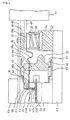
- FIG. 1 is a section view showing the structure of a compression bonded type semiconductor device according to a first mode of the present invention. It is a section view showing the structure of the compression bonded type semiconductor device as a system including a gate drive device for controlling a compression bonded type semiconductor device such as GCT into the GCT.
- the reference numeral (31) denotes the GCT and (32) a disk semiconductor device.
- a gate electrode 32a made of aluminum is formed at the outer peripheral part, on the surface of the semiconductor substrate 32, a cathode electrode 32b made of aluminum is formed inside the gate electrode 32a and an anode electrode 32c made of aluminum is formed on the back of the gate electrode 32a.
- the reference numerals (33 and 34) denote a cathode distortion buffer disk made of molybdenum and an external cathode electrode made of copper mounted one after another on the surface of the semiconductor substrate 32 at the cathode electrode 32b side, (35 and 36) an anode distortion buffer disk made of molybdenum and an external anode electrode made of copper mounted one after another at the anode electrode 32c side, (37) a ring gate electrode made mainly of copper, molybdenum, stainless steel or the like which abuts against the gate electrode 32a of the semiconductor substrate 32, (38) an external gate terminal made of non-magnetic ring-shaped plate mainly made of materials which is not affected to electromagnetic induction such as copper, molybdenum, tungsten or their alloy such as phosphor bronze.
- the reference numeral (39) denotes an elastic body such as a disc spring or wave spring which presses the ring gate electrode 37 to the gate electrode 32a together with the external gate electrode 38 via an annular insulator 40, (41) an insulator made of an insulating sheet such as polyimide and provided between the ring gate electrode 37, the external gate terminal 38 and the external cathode electrode 34.
- the reference numeral (46) denotes a first stack electrode for pressing the GCT 31 from the external cathode electrode 34, (47) a second stack electrode for pressing the GCT 31 from the external anode electrode 36 side and extending below the connection portion 38b where the external gate terminal 38 is electrically connected with a plate-shaped control gate electrode 49 described later.
- the reference numeral (48) denotes the plate-shaped control electrode made of a ringed metal plate disposed concentrically with the external gate terminal 38 and pressed to the external cathode electrode 34 by the first stack electrode 46, (49) a plate-shaped control gate electrode made of a ringed metal plate which is disposed concentrically with the external gate terminal 38 and whose inner peripheral part is electrically connected with the outer peripheral part of the external gate terminal 38 and (50) an insulation sleeve for insulating the plate-shaped control electrode 48 from the plate-shaped control gate electrode 49. It is fixed to the plate-shaped control electrode 48 and the plate-shaped control gate electrode 49 by a fastener 51 such as a bolt.
- the plate-shaped control electrode 48 and the plate-shaped control gate electrode 49 are both connected to a gate drive device 52 for controlling the GCT 31.
- the reference numeral (53) denotes a ringed support member which is disposed concentrically with the external gate terminal 38 between the connection section 38b where the external gate terminal 38 and the plate-shaped control gate electrode 49 are electrically connected and the second stack electrode 47 and which presses the connection section 38b.
- This support member 53 contains an elastic body 54 formed into a ring by a disc spring or wave spring and is composed of a ringed gate terminal holding plate 55 made of metal pressing the connection section 38b and a ringed second insulator 56 provided between the second stack electrode 47 and the gate terminal holding plate 55 to electrically insulate the second stack electrode 47 from the gate terminal holding plate 55.
- the GCT 31 may be turned on by igniting main current flowing from the external anode electrode 36 to the external cathode electrode 34 by isotropically supplying gate current from the whole circumferential plane from the gate drive device 52 to the external gate terminal 38 of the GCT 31. It may be also turned off by instantly extinguishing the main current by supplying gate current in the reverse direction from that of turn-on.
- a current transient fall inclination of the gate current at the time of turn-off is about 6,000 A/ ⁇ s, thus enabling the increase of switching speed together with a transient rise inclination of about 1,000 A/ ⁇ s at the time of turn-on.
- connection section 38b connecting the external gate terminal 38 with the plate-shaped control gate electrode 49 which forms a part of a feeding path from the external cathode electrode 34 to the plate-shaped control gate electrode 49 must be fully done in order to feed the large current instantly at the time of turn-on or turn-off as described above.
- the second stack electrode 47 is extended below the connection section 38b where the external gate terminal 38 is electrically connected with the plate-shaped control gate electrode 49 and there is provided the support member 53 having the second elastic body 54 which is disposed concentrically with the external gate terminal 38 between the connection section 38b where the external gate terminal 38 and the plate-shaped control gate electrode 49 are electrically connected and the second stack electrode 47 to press the connection section 38b.
- the members provided to fix the external gate terminal 8 to the plate-shaped control gate electrode 18 in the prior art GCT of 6 kV/6kA of rate for example, i.e., 24 attachment holes 8c, the holding plate 23 and the fastener 24, may be eliminated because the support member 53 presses the connection section 38b. Therefore, it becomes possible to attach/remove the GCT simply to/from the plate-shaped control gate electrode.
- connection section 38b of the outer peripheral part of the external gate terminal 38 and the inner peripheral part of the plate-shaped control gate electrode 49 may be pressed uniformly, thus preventing the contact of the connection section 38b from becoming point-to-point contact and eliminating the possibility of permanent destruction of the GCT which is otherwise caused as current concentrates locally.
- the positional relationship between the gate holding plate 55 containing an elastic body 54 and the second insulator 56 may be up side down and may bring about the same effect.
- first stack electrode 46 may be extended to the connection section 38b similarly to the second stack electrode 47. It also brings about the same effect as described above.
- the gate drive device may be an external control unit so long as it controls the gate current.
- a control gate electrode which can be connected to the external control unit may have a shape other than the plate-shape.
- FIG. 2A the reference numeral (53a) denotes a ringed support member disposed concentrically with the external gate terminal 38 between the connection section 38b and the second stack electrode 47 to press the connection section 38b.
- the support member 53a is composed of a ringed gate terminal holding plate 55a made of metal which abuts to the external gate terminal 38 and a ringed second insulator 56a which contains a second elastic body 54 for electrically insulating the second stack electrode 47 from the gate terminal holding plate 55a and brings about the same effect as described above.
- the second insulator 56a is constructed so as to include the second elastic body 54 from the external gate terminal 38 side and the second stack electrode 47 side. Its end on the external gate terminal 38 side is fixed to the gate terminal holding plate 55a by a bolt 57 and presses the connection section 38b by the urging force of the second elastic body 54.
- the reference numeral (53b) denotes a ringed support member disposed concentrically with the external gate terminal 38 between the connection section 38b and the second stack electrode 47 to press the connection section 38b.
- the support member 53b is composed of a ringed gate terminal holding plate 55b made of metal which abuts to the external gate terminal 38 and a ringed second insulator 56b which contains a second elastic body 54, is provided between the second stack electrode 47 and the gate terminal holding plate 55b to electrically insulate the second stack electrode 47 from the gate terminal holding plate 55b and brings about the same effect as described above.
- the reference numeral (53c) denotes a ringed support member disposed concentrically with the external gate terminal 38 between the connection section 38b and the second stack electrode 47 to press the connection section 38b.
- the support member 53c is composed of a ringed second insulator 56c made of an insulator which contains the second elastic body 54 and is provided between the connection section 38b and the second stack electrode 46 to electrically insulate the second stack electrode 47 from the external gate terminal 38. It also brings about the same effect with what described above.
- six bolts 58 at most may be attached from the gate terminal holding plate 55 side in order to improve the contact of the connection section 38b between the external gate terminal 38 and a plate-shaped control gate electrode 49 as shown in FIG. 3.
- the gate electrode 32a has been formed at the outer peripheral part on the surface of the semiconductor substrate 32 as one example of the gate structure of the GCT 31 of the first embodiment, the gate electrode may be formed at the middle section of the surface. It also brings about the same effect.
- FIG. 4 is a perspective view showing the partially-cut-away structure of the compression bonded type semiconductor device according to the second mode of the invention. What is different in FIG. 4 from those in FIG. 1 is that a heat release mechanism is provided in the support member. That is, the reference numeral (61) denotes a ringed support member disposed concentrically with the external gate terminal 38 between the connection section 38b where the external gate terminal 38 is electrically connected with the plate-shaped control gate electrode 48 and the second stack electrode 47 to press the connection section 38b.
- This support member 61 comprises a ringed gate terminal holding plate 63 formed of metal which abuts to the plate-shaped control gate electrode 48, e.g., metal on which soft metal is coated on oxygen free copper, and having a heat release mechanism 62, a second ringed elastic body 54 made of a disc spring or wave spring and a second insulator 64 containing the second elastic body 54 and provided between the second stack electrode 47 and the gate terminal holding plate 63 to electrically insulate the second stack electrode 47 from the gate terminal holding plate 63.
- the heat release mechanism 62 is constructed by circulating coolant water within a ringed water passage 65 provided within the gate terminal holding plate 63.
- the beat release mechanism 62 is provided in the support member 61.
- Such structure allows heat of the gate electrode 32a section to be cooled by the heat release mechanism 62 via the ring gate electrode 37 and the external gate terminal 38. Therefore, it becomes possible to suppress the in-plane temperature distribution of the semiconductor substrate 32 of the GCT 31 from becoming non-uniform.
- the water cooling type heat release mechanism is adopted. Such structure also allows the heat of the gate electrode 32a section to be cooled efficiently by the heat release mechanism 62 via the ring gate electrode 37 and the external gate terminal 38. Therefore, it becomes possible to suppress the in-plane temperature distribution of the semiconductor substrate 32 of the GCT 31 from becoming non-uniform.
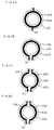
- FIG. 5A a heat release mechanism 62a is constructed so that there is one each inlet and outlet of coolant water 66, the water flow of the coolant water 66 is divided into two directions at the inlet and the water flows within a water passage 65 provided in the gate terminal holding plate 63a and is combined again at the outlet.
- FIG. 5B a heat release mechanism 62b is constructed so that there is one each inlet and outlet of coolant water 66 and the water flow of the coolant water 66 flows so as to circulate within a water passage 65b provided in a gate terminal holding plate 63b.
- FIG. 5A a heat release mechanism 62a is constructed so that there is one each inlet and outlet of coolant water 66, the water flow of the coolant water 66 flows so as to circulate within a water passage 65b provided in a gate terminal holding plate 63b.
- a heat release mechanism 62c is constructed so that there are two each inlet and outlet of coolant water 66 and the water flow of the coolant water 66 flows so as to circulate partially within water passages 65c provided in a gate terminal holding plate 63c in the same direction from each other.
- a heat release mechanism 62d is constructed so that there are two each inlet and outlet of coolant water 66 and the water flow of the coolant water 66 flows so as to circulate partially within water passages 65d provided in a gate terminal holding plate 63d in the opposite direction from each other.
- the heat release mechanisms in FIGs. 5A, 5B, 5C and 5D also bring about the same effects as in second mode.
- the inventive compression bonded type semiconductor device is suitable for quickly turning on/off large current of the main circuit by the gate control.
- it is suitable for BTB (Bus Tie Breaker) and SVG (Static Var Generator) as an application to electric power, for driving a large capacity inverter for paper or steel making rolling mill as an application to industrial use, for a ground transformer station as an application to rail railways and for a high voltage large capacity switch, etc.
Landscapes
- Thyristors (AREA)
- Die Bonding (AREA)
Abstract
Description
Claims (7)
- A compression bonded type semiconductor device, comprising:a compression bonded type semiconductor element having a semiconductor substrate wherein a gate electrode and a cathode electrode are formed on the surface thereof and art anode electrode is formed on the back thereof, an insulating cylinder containing said semiconductor substrate, a ring gate electrode which abuts to said gate electrode and an external gate terminal whose outer peripheral part projects out of the side of said insulating cylinder and is secured to said insulating cylinder and whose inner peripheral part abuts to said ring gate electrode;a control gate electrode which can be connected to an external controller electrically connected with said external gate terminal;a support member disposed concentrically with said external gate terminal and having an elastic body which presses a connection section where said external gate terminal is electrically connected with said control gate electrode; anda stack electrode for compressing said compression bonded type semiconductor element and for supporting said support member.
- The compression bonded type semiconductor device as described in Claim 1, characterized in that said elastic body is formed into a ringed-shape.
- The compression bonded type semiconductor device as described in Claim 1, characterized in that a heat release mechanism is provided in the support member.
- The compression bonded type semiconductor device as described in Claim 3, characterized in that said heat release mechanism is a water cooling type mechanism.
- A compression bonded type semiconductor device, comprising:a compression bonded type semiconductor element having a disc-shaped semiconductor substrate wherein a gate electrode is formed on the outer peripheral part of the surface thereof, a cathode electrode is formed inside of said gate electrode and an anode electrode is formed on the back thereof, an external cathode electrode disposed so as to be able to press said cathode electrode, an external anode electrode disposed so as to be able to press said anode electrode, an insulating cylinder containing said semiconductor substrate, an annular ring gate electrode which abuts to said gate electrode and an external gate terminal made of an annular plate which projects out of the side of said insulating cylinder and is secured to said insulating cylinder and whose inner peripheral part abuts to said ring gate electrode;a plate-shaped control electrode disposed concentrically with said external gate terminal and is electrically connected with said external cathode electrode, a plate-shaped control gate electrode disposed concentrically with said external gate terminal and is electrically connected with said external gate terminal at the inner peripheral part thereof and a gate drive device for controlling gate current to which said plate-shaped control electrode and said plate-shaped control gate electrode are fixed via a first insulator to connect with said plate-shaped control electrode and said plate-shaped control gate electrode;a stack electrode composed of a first stack electrode for compressing said compression bonded type semiconductor element from said external cathode electrode and a second stack electrode which compresses said compression bonded type semiconductor element from said external anode electrode and which extends below a connection section where said external gate terminal is electrically connected with said plate-shaped control gate electrode; anda support member disposed concentrically with said external gate terminal between the connection section where said external gate terminal is electrically connected with said plate-shaped control gate electrode and said second stack electrode and having an annular elastic body which presses said connection section and a second insulator for electrically insulating said second stack electrode and said external gate terminal.
- The compression bonded type semiconductor device as described in Claim 5, characterized in that a heat release mechanism is provided in the support member.
- The compression bonded type semiconductor device as described in Claim 6, characterized in that said heat release mechanism is a water cooling type mechanism.
Applications Claiming Priority (1)
| Application Number | Priority Date | Filing Date | Title |
|---|---|---|---|
| PCT/JP1999/000120 WO2000042664A1 (en) | 1999-01-18 | 1999-01-18 | Compression bonded semiconductor device |
Publications (3)
| Publication Number | Publication Date |
|---|---|
| EP1065730A1 true EP1065730A1 (en) | 2001-01-03 |
| EP1065730A4 EP1065730A4 (en) | 2004-05-26 |
| EP1065730B1 EP1065730B1 (en) | 2006-11-29 |
Family
ID=14234722
Family Applications (1)
| Application Number | Title | Priority Date | Filing Date |
|---|---|---|---|
| EP99900329A Expired - Lifetime EP1065730B1 (en) | 1999-01-18 | 1999-01-18 | Compression contacted semiconductor device |
Country Status (5)
| Country | Link |
|---|---|
| US (1) | US6303987B1 (en) |
| EP (1) | EP1065730B1 (en) |
| JP (1) | JP3571354B2 (en) |
| DE (1) | DE69934220T2 (en) |
| WO (1) | WO2000042664A1 (en) |
Cited By (2)
| Publication number | Priority date | Publication date | Assignee | Title |
|---|---|---|---|---|
| WO2007054368A3 (en) * | 2005-11-14 | 2007-07-26 | Peter Koellensperger | Semiconductor device comprising a housing containing a triggering unit |
| CN103346130A (en) * | 2013-07-01 | 2013-10-09 | 株洲南车时代电气股份有限公司 | GCT gate pole insulating base and gate pole component |
Families Citing this family (8)
| Publication number | Priority date | Publication date | Assignee | Title |
|---|---|---|---|---|
| CA3038491A1 (en) | 2008-10-07 | 2010-04-15 | REG Life Sciences, LLC | Bacterial host cells engineered to express a carboxylic acid reductase and a thioesterase |
| KR20130100630A (en) * | 2012-03-02 | 2013-09-11 | 삼성전자주식회사 | Electron emission device and x-ray generator including the same |
| KR20140106291A (en) * | 2013-02-26 | 2014-09-03 | 삼성전자주식회사 | X-ray imaging system having flat panel type X-ray generator, and X-ray generator, and electron emission device |
| JP2015138835A (en) * | 2014-01-21 | 2015-07-30 | 株式会社東芝 | Semiconductor device |
| JP6320564B2 (en) | 2014-04-10 | 2018-05-09 | アーベーベー・シュバイツ・アーゲー | Turn-off power semiconductor with improved gate ring centering and locking and method of manufacturing the same |
| JP2016062983A (en) * | 2014-09-16 | 2016-04-25 | 株式会社東芝 | Semiconductor device |
| CN111755446A (en) * | 2019-03-29 | 2020-10-09 | 长鑫存储技术有限公司 | a semiconductor structure |
| CN111933588B (en) * | 2020-06-24 | 2022-04-29 | 株洲中车时代半导体有限公司 | An IGCT packaging structure |
Family Cites Families (11)
| Publication number | Priority date | Publication date | Assignee | Title |
|---|---|---|---|---|
| DE2705476A1 (en) * | 1977-02-10 | 1978-08-17 | Bbc Brown Boveri & Cie | Liq. cooled powder semiconductor - has wafer compressed between two cooling capsules, with pressure applied to their outer surfaces |
| JPS5633886A (en) * | 1979-08-28 | 1981-04-04 | Mitsubishi Electric Corp | Light drive semiconductor device |
| JP2868209B2 (en) | 1985-08-05 | 1999-03-10 | 富士通株式会社 | Memory protection device in multiprocessor system |
| JPH0526773Y2 (en) * | 1985-08-12 | 1993-07-07 | ||
| JPH0760893B2 (en) * | 1989-11-06 | 1995-06-28 | 三菱電機株式会社 | Semiconductor device and manufacturing method thereof |
| JPH04352457A (en) * | 1991-05-30 | 1992-12-07 | Mitsubishi Electric Corp | Semiconductor device and manufacture thereof |
| US5371386A (en) * | 1992-04-28 | 1994-12-06 | Mitsubishi Denki Kabushiki Kaisha | Semiconductor device and method of assembling the same |
| JP3153638B2 (en) * | 1992-06-26 | 2001-04-09 | 三菱電機株式会社 | Pressure contact type semiconductor device, method of manufacturing the same, and heat compensator |
| JP3469304B2 (en) * | 1994-04-12 | 2003-11-25 | 三菱電機株式会社 | Semiconductor device |
| JP3291977B2 (en) * | 1995-05-31 | 2002-06-17 | 三菱電機株式会社 | Pressure contact type semiconductor element, method of manufacturing the same, and pressure contact type semiconductor device |
| JP3535341B2 (en) * | 1997-03-24 | 2004-06-07 | 三菱電機株式会社 | Pressure welding type semiconductor device |
-
1999
- 1999-01-18 JP JP55392999A patent/JP3571354B2/en not_active Expired - Lifetime
- 1999-01-18 WO PCT/JP1999/000120 patent/WO2000042664A1/en not_active Ceased
- 1999-01-18 DE DE69934220T patent/DE69934220T2/en not_active Expired - Lifetime
- 1999-01-18 EP EP99900329A patent/EP1065730B1/en not_active Expired - Lifetime
-
2000
- 2000-09-18 US US09/664,574 patent/US6303987B1/en not_active Expired - Lifetime
Cited By (3)
| Publication number | Priority date | Publication date | Assignee | Title |
|---|---|---|---|---|
| WO2007054368A3 (en) * | 2005-11-14 | 2007-07-26 | Peter Koellensperger | Semiconductor device comprising a housing containing a triggering unit |
| CN103346130A (en) * | 2013-07-01 | 2013-10-09 | 株洲南车时代电气股份有限公司 | GCT gate pole insulating base and gate pole component |
| CN103346130B (en) * | 2013-07-01 | 2015-11-11 | 株洲南车时代电气股份有限公司 | GCT gate insulation seat and gate pole assembly |
Also Published As
| Publication number | Publication date |
|---|---|
| WO2000042664A1 (en) | 2000-07-20 |
| US6303987B1 (en) | 2001-10-16 |
| JP3571354B2 (en) | 2004-09-29 |
| EP1065730A4 (en) | 2004-05-26 |
| EP1065730B1 (en) | 2006-11-29 |
| DE69934220D1 (en) | 2007-01-11 |
| DE69934220T2 (en) | 2007-10-04 |
Similar Documents
| Publication | Publication Date | Title |
|---|---|---|
| US5345096A (en) | Turn-off high-power semiconductor component with low inductive housing | |
| EP1065730B1 (en) | Compression contacted semiconductor device | |
| US5278434A (en) | Pressure engagement structure for a full press-pack type semiconductor device | |
| EP0746021B1 (en) | Compression bonded type semiconductor element and manufacturing method for the same | |
| JPWO2010150390A1 (en) | Gas insulated switchgear | |
| JPWO2000042664A1 (en) | Pressure-welded semiconductor device | |
| JP2002222916A (en) | Pressure welding type semiconductor device | |
| JP4129082B2 (en) | Pressure contact type semiconductor device, ring-shaped gate terminal thereof, and power application device | |
| JPH0353729B2 (en) | ||
| US6441407B1 (en) | Gate controlled thyristor driven with low-inductance | |
| JPH03119762A (en) | Pressure-welding type semiconductor device for electric power | |
| PL117388B1 (en) | Thyristor with amplifying gate equipped with boosting gate for switch-offjj ventil'nojj skhemojj,sposobstvujuhhejj wykljucheniju | |
| JP3609430B2 (en) | Pressure contact type semiconductor device | |
| JP3351537B2 (en) | Pressure welding type semiconductor device | |
| JPWO2000042663A1 (en) | Pressure-welded semiconductor device | |
| EP0249324B1 (en) | High-power switch | |
| JPWO2000016394A1 (en) | Pressure-welded semiconductor device | |
| EP0631321A1 (en) | Gate turn-off thyristor | |
| JPH10290001A (en) | Gate turn-off thyristor | |
| JP3422211B2 (en) | Semiconductor switching device, semiconductor stack device and power conversion device using the same | |
| JP3371068B2 (en) | Semiconductor switching device, semiconductor stack device and power conversion device using the same | |
| JP2000004016A (en) | Pressure contact type semiconductor device | |
| JPH1065100A (en) | Gate turn-off thyristor stack | |
| JP2003032091A (en) | Semiconductor switching equipment for power devices | |
| JPH01102933A (en) | Pressure-contact flat type semiconductor device |
Legal Events
| Date | Code | Title | Description |
|---|---|---|---|
| PUAI | Public reference made under article 153(3) epc to a published international application that has entered the european phase |
Free format text: ORIGINAL CODE: 0009012 |
|
| 17P | Request for examination filed |
Effective date: 20000828 |
|
| AK | Designated contracting states |
Kind code of ref document: A1 Designated state(s): CH DE FR GB IT LI |
|
| A4 | Supplementary search report drawn up and despatched |
Effective date: 20040415 |
|
| 17Q | First examination report despatched |
Effective date: 20040716 |
|
| RAP1 | Party data changed (applicant data changed or rights of an application transferred) |
Owner name: MITSUBISHI DENKI KABUSHIKI KAISHA |
|
| RTI1 | Title (correction) |
Free format text: COMPRESSION CONTACTED SEMICONDUCTOR DEVICE |
|
| GRAP | Despatch of communication of intention to grant a patent |
Free format text: ORIGINAL CODE: EPIDOSNIGR1 |
|
| GRAS | Grant fee paid |
Free format text: ORIGINAL CODE: EPIDOSNIGR3 |
|
| GRAA | (expected) grant |
Free format text: ORIGINAL CODE: 0009210 |
|
| RIN1 | Information on inventor provided before grant (corrected) |
Inventor name: SATOH, KATSUMI,MITSUBISHI DENKI K.K. Inventor name: KAWAMURA, TOSHINOBU,MITSUBISCHI DENKI K.K. |
|
| AK | Designated contracting states |
Kind code of ref document: B1 Designated state(s): CH DE FR GB IT LI |
|
| PG25 | Lapsed in a contracting state [announced via postgrant information from national office to epo] |
Ref country code: IT Free format text: LAPSE BECAUSE OF FAILURE TO SUBMIT A TRANSLATION OF THE DESCRIPTION OR TO PAY THE FEE WITHIN THE PRESCRIBED TIME-LIMIT;WARNING: LAPSES OF ITALIAN PATENTS WITH EFFECTIVE DATE BEFORE 2007 MAY HAVE OCCURRED AT ANY TIME BEFORE 2007. THE CORRECT EFFECTIVE DATE MAY BE DIFFERENT FROM THE ONE RECORDED. Effective date: 20061129 |
|
| REG | Reference to a national code |
Ref country code: GB Ref legal event code: FG4D |
|
| REG | Reference to a national code |
Ref country code: CH Ref legal event code: EP |
|
| RIN2 | Information on inventor provided after grant (corrected) |
Inventor name: SATOH, KATSUMI,MITSUBISHI DENKI K.K. Inventor name: KAWAMURA, TOSHINOBU, C/O MITSUBISCHI DENKI K.K. |
|
| REF | Corresponds to: |
Ref document number: 69934220 Country of ref document: DE Date of ref document: 20070111 Kind code of ref document: P |
|
| REG | Reference to a national code |
Ref country code: CH Ref legal event code: NV Representative=s name: BOVARD AG PATENTANWAELTE |
|
| EN | Fr: translation not filed | ||
| PLBE | No opposition filed within time limit |
Free format text: ORIGINAL CODE: 0009261 |
|
| STAA | Information on the status of an ep patent application or granted ep patent |
Free format text: STATUS: NO OPPOSITION FILED WITHIN TIME LIMIT |
|
| GBPC | Gb: european patent ceased through non-payment of renewal fee |
Effective date: 20070228 |
|
| 26N | No opposition filed |
Effective date: 20070830 |
|
| PG25 | Lapsed in a contracting state [announced via postgrant information from national office to epo] |
Ref country code: GB Free format text: LAPSE BECAUSE OF NON-PAYMENT OF DUE FEES Effective date: 20070228 Ref country code: FR Free format text: LAPSE BECAUSE OF FAILURE TO SUBMIT A TRANSLATION OF THE DESCRIPTION OR TO PAY THE FEE WITHIN THE PRESCRIBED TIME-LIMIT Effective date: 20070720 |
|
| PG25 | Lapsed in a contracting state [announced via postgrant information from national office to epo] |
Ref country code: FR Free format text: LAPSE BECAUSE OF FAILURE TO SUBMIT A TRANSLATION OF THE DESCRIPTION OR TO PAY THE FEE WITHIN THE PRESCRIBED TIME-LIMIT Effective date: 20061129 |
|
| REG | Reference to a national code |
Ref country code: CH Ref legal event code: PFA Owner name: MITSUBISHI DENKI KABUSHIKI KAISHA Free format text: MITSUBISHI DENKI KABUSHIKI KAISHA#7-3, MARUNOUCHI 2-CHOME#CHIYODA-KU TOKYO 100-8310 (JP) -TRANSFER TO- MITSUBISHI DENKI KABUSHIKI KAISHA#7-3, MARUNOUCHI 2-CHOME#CHIYODA-KU TOKYO 100-8310 (JP) |
|
| PGFP | Annual fee paid to national office [announced via postgrant information from national office to epo] |
Ref country code: CH Payment date: 20140114 Year of fee payment: 16 |
|
| REG | Reference to a national code |
Ref country code: CH Ref legal event code: PL |
|
| PG25 | Lapsed in a contracting state [announced via postgrant information from national office to epo] |
Ref country code: LI Free format text: LAPSE BECAUSE OF NON-PAYMENT OF DUE FEES Effective date: 20150131 Ref country code: CH Free format text: LAPSE BECAUSE OF NON-PAYMENT OF DUE FEES Effective date: 20150131 |
|
| PGFP | Annual fee paid to national office [announced via postgrant information from national office to epo] |
Ref country code: DE Payment date: 20180103 Year of fee payment: 20 |
|
| REG | Reference to a national code |
Ref country code: DE Ref legal event code: R071 Ref document number: 69934220 Country of ref document: DE |