EP1062632B1 - Mobiler datenträger - Google Patents
Mobiler datenträger Download PDFInfo
- Publication number
- EP1062632B1 EP1062632B1 EP99965561.6A EP99965561A EP1062632B1 EP 1062632 B1 EP1062632 B1 EP 1062632B1 EP 99965561 A EP99965561 A EP 99965561A EP 1062632 B1 EP1062632 B1 EP 1062632B1
- Authority
- EP
- European Patent Office
- Prior art keywords
- data processing
- processing circuit
- current
- supply
- voltage
- Prior art date
- Legal status (The legal status is an assumption and is not a legal conclusion. Google has not performed a legal analysis and makes no representation as to the accuracy of the status listed.)
- Expired - Lifetime
Links
Images



Classifications
-
- G—PHYSICS
- G06—COMPUTING OR CALCULATING; COUNTING
- G06K—GRAPHICAL DATA READING; PRESENTATION OF DATA; RECORD CARRIERS; HANDLING RECORD CARRIERS
- G06K19/00—Record carriers for use with machines and with at least a part designed to carry digital markings
- G06K19/06—Record carriers for use with machines and with at least a part designed to carry digital markings characterised by the kind of the digital marking, e.g. shape, nature, code
- G06K19/067—Record carriers with conductive marks, printed circuits or semiconductor circuit elements, e.g. credit or identity cards also with resonating or responding marks without active components
- G06K19/07—Record carriers with conductive marks, printed circuits or semiconductor circuit elements, e.g. credit or identity cards also with resonating or responding marks without active components with integrated circuit chips
-
- G—PHYSICS
- G06—COMPUTING OR CALCULATING; COUNTING
- G06K—GRAPHICAL DATA READING; PRESENTATION OF DATA; RECORD CARRIERS; HANDLING RECORD CARRIERS
- G06K19/00—Record carriers for use with machines and with at least a part designed to carry digital markings
- G06K19/06—Record carriers for use with machines and with at least a part designed to carry digital markings characterised by the kind of the digital marking, e.g. shape, nature, code
- G06K19/067—Record carriers with conductive marks, printed circuits or semiconductor circuit elements, e.g. credit or identity cards also with resonating or responding marks without active components
- G06K19/07—Record carriers with conductive marks, printed circuits or semiconductor circuit elements, e.g. credit or identity cards also with resonating or responding marks without active components with integrated circuit chips
- G06K19/0701—Record carriers with conductive marks, printed circuits or semiconductor circuit elements, e.g. credit or identity cards also with resonating or responding marks without active components with integrated circuit chips at least one of the integrated circuit chips comprising an arrangement for power management
-
- G—PHYSICS
- G06—COMPUTING OR CALCULATING; COUNTING
- G06K—GRAPHICAL DATA READING; PRESENTATION OF DATA; RECORD CARRIERS; HANDLING RECORD CARRIERS
- G06K19/00—Record carriers for use with machines and with at least a part designed to carry digital markings
- G06K19/06—Record carriers for use with machines and with at least a part designed to carry digital markings characterised by the kind of the digital marking, e.g. shape, nature, code
- G06K19/067—Record carriers with conductive marks, printed circuits or semiconductor circuit elements, e.g. credit or identity cards also with resonating or responding marks without active components
- G06K19/07—Record carriers with conductive marks, printed circuits or semiconductor circuit elements, e.g. credit or identity cards also with resonating or responding marks without active components with integrated circuit chips
- G06K19/0723—Record carriers with conductive marks, printed circuits or semiconductor circuit elements, e.g. credit or identity cards also with resonating or responding marks without active components with integrated circuit chips the record carrier comprising an arrangement for non-contact communication, e.g. wireless communication circuits on transponder cards, non-contact smart cards or RFIDs
-
- G—PHYSICS
- G06—COMPUTING OR CALCULATING; COUNTING
- G06K—GRAPHICAL DATA READING; PRESENTATION OF DATA; RECORD CARRIERS; HANDLING RECORD CARRIERS
- G06K19/00—Record carriers for use with machines and with at least a part designed to carry digital markings
- G06K19/06—Record carriers for use with machines and with at least a part designed to carry digital markings characterised by the kind of the digital marking, e.g. shape, nature, code
- G06K19/067—Record carriers with conductive marks, printed circuits or semiconductor circuit elements, e.g. credit or identity cards also with resonating or responding marks without active components
- G06K19/07—Record carriers with conductive marks, printed circuits or semiconductor circuit elements, e.g. credit or identity cards also with resonating or responding marks without active components with integrated circuit chips
- G06K19/073—Special arrangements for circuits, e.g. for protecting identification code in memory
- G06K19/07309—Means for preventing undesired reading or writing from or onto record carriers
- G06K19/07363—Means for preventing undesired reading or writing from or onto record carriers by preventing analysis of the circuit, e.g. dynamic or static power analysis or current analysis
Definitions
- the invention relates to a mobile data carrier, in particular a chip card.
- a mobile data carrier in particular a chip card.
- smart cards have become known under the name smart card.
- EP 0 874 327 A2 shows a smart card having means for detecting the level of a voltage provided by an external device, wherein an activation signal is generated when the detected voltage is below a predetermined level, and a voltage regulation means which detects the levels of the provided voltage in the operating voltage level of the smart card converted in response to the activation signal.
- US 5,045,770 shows a control device for receiving electrical energy from an external magnetic alternating field by means of an inductive resonant circuit and outputting a regulated output voltage whose output power is controlled by means of input power diversion, wherein separate current paths are provided for the branch current and the output current and a rectifier device is provided in the output current path ,
- US 5,495,241 shows a method and a device for reducing losses in contactless data and energy transfer devices, wherein a functional unit is provided in a movable part, which determines the current losses in a voltage control device, wherein a stationary part, when a set value is exceeded, the Can reduce energy input.
- US 4,881,199 relates to a read circuit for integrated logic circuits with a memory which consists of a matrix of memory cells, the reading being carried out by detecting a change in current or voltage.
- the invention has the object of at least significantly complicating, if not impossible, the exploration of data patterns by the aforementioned method in a mobile data carrier.
- a mobile data carrier in particular a chip card, having a data processing circuit and a supply arrangement for supplying electrical energy to supply voltage terminals for operating the data processing circuit from an external energy source located outside the data carrier, wherein the supply arrangement comprises a voltage-limiting control circuit connected to the supply voltage terminals the data processing circuit is arranged in parallel, and a current control arrangement which is arranged in series with respect to the power supply to the data processing circuit with the parallel arrangement of the voltage-limiting control circuit and the data processing circuit.
- the invention achieves in a simple and advantageous manner that a constant energy flow is always fed into the data carrier from an external energy source arranged outside the data carrier.
- the voltage and the current with which this energy flow is effected are always constant at points accessible from outside the data carrier during the entire operation and thus can not be used as a basis for individual data processing operations within the system Data processing circuit to. In particular, it is no longer possible to deduce the exact execution of a specific calculation from the energy flow.
- the invention has the function of a supply source with the characteristics that the load is independent of the load at the receiving end of the path in the arrangement over which the energy flow to the data processing circuit the feeding side of this path is and that the source on the feeding side behaves like a power source over a wide range of control.
- a supply source can be constructed by a parallel regulator.
- the contactless energy supply of a chip card has the characteristic of a constant current source without having to be regulated.
- the current control arrangement is arranged to provide an at least almost load-independent supply current and that the voltage-limiting control circuit is designed to receive an excess current, which complements with respect to the supply current to a recorded from the data processing circuit to the supply voltage terminals supply current is.
- the mobile data carrier according to the invention is characterized in that the supplied from the power control arrangement supply current is controlled at least almost exclusively by a voltage output from the external power source voltage.
- the data processing circuit is formed with asynchronously operating logic elements whose signal processing speed is dependent on a voltage applied to the supply voltage terminals of the data processing circuit supply voltage.
- a Confusion in unauthorized access can be achieved.
- the signal processing speed of the logic elements is advantageously dependent on the supply voltage.
- the data throughput of the data processing circuit is thus automatically adapted to the available supply voltage.
- Such a trained data processing circuit is functional over a wide supply voltage range at comparatively low circuit complexity.
- the inventive, mobile data carrier has the further advantage that no interference of signals from the data processing circuit with signals that are supplied to the mobile data carrier from outside or the mobile data carrier emits to the outside.
- the protection against the aforementioned investigation method is particularly high, since not even the electromagnetic radiation of the data processing circuit in the mobile data carrier contains information about data patterns in the data processing circuit.
- the supply current consumed by the mobile data carrier is independent of the processed data patterns.
- the processing speed in the data processing circuit is always set to the optimum possible value.
- a much smaller dimensioned filter capacitor can be used for interference suppression.
- the arrangement after Fig. 1 comprises a data processing circuit 1 with two supply voltage terminals 2, 3. About this data processing circuit 1 is supplied to a supply voltage, which serves the power supply to the data processing circuit 1. From an external, outside the disk and arranged in Fig.1 not shown energy source is supplied electrical energy via two terminals 4, 5. For example, the terminals 4, 5 are connected to a circuit arrangement which rectifies a transmitted electrical voltage in a contactless chip card and provides this rectified voltage for supplying power to the data processing circuit 1.
- the terminals 4, 5 form inputs of a feed arrangement 6 which comprises a voltage-limiting control circuit 7 and a current control arrangement 8.
- the voltage-limiting control circuit 7 is arranged parallel to the supply voltage terminals 2, 3.
- the current control device 8 is arranged in series with the parallel circuit of the voltage-limiting control circuit 7 and the data processing circuit 1. This series arrangement is arranged between the terminals 4 and 5.
- the current control assembly 8 is arranged to provide at least a virtually load-independent supply current, which in Fig. 1 is indicated by the arrow with the reference numeral 9. At least in a certain modulation range, the current control arrangement 8 thus has the behavior of an at least approximately ideal current source.
- the supply current 9 can be controlled at most by a voltage applied between the terminals 4 and 5 voltage to adjust the power supply to the data processing circuit 1 of this voltage between the terminals 4 and 5.
- the data processing circuit 1 is preferably formed with asynchronous logic elements whose signal processing speed is dependent on the available supply current 9 as a maximum supply current to the supply voltage terminals 2, 3.
- the supply current in Fig. 1 denoted by the arrow 10
- An excess current represented by the arrow 11 in FIG Fig. 1 which is complementary to the supply current 10 with respect to the supply current 9, flows through the voltage-limiting one Control circuit 7 from.
- the supply current 9 can be dimensioned independently of data.
- a capacitor 12 is also arranged, which is used in particular for contactless smart cards to avoid interference between signals in the data processing circuit 1 and signals that are received by the smart card from outside or transmitted to the outside.
- this capacitor 12 can be very small dimensions.
- the voltage-limiting control circuit 7 has in addition to the inclusion of the excess current 11, the function to keep the supply voltage to the supply voltage terminals 2, 3 within a predetermined voltage range.
- the capacitor 12 also serves for averaging, i. To compensate for peak load in the data processing circuit 1. Since these can be greatly reduced by using asynchronous logic elements, only a small capacitor is required for this purpose.
- Fig. 1 With the structure according to Fig. 1 can be dispensed with for regulating data-dependent supply currents to a control loop, which always has a finite control speed and thus can not cause a complete suppression of such data dependencies in the energy supply by design.
- the supply current 9 is completely constant without data dependence.
- the voltage-limiting operation of the control circuit 7 ensures that the current control arrangement 8 remains in its control range even with fluctuating supply currents 10 and thus the supply current 9 can be kept constant.
- the supply current 9 can be adapted to the supply current supply voltage characteristic of the data processing circuit 1.
- Fig. 2 shows a simplified, block schematic representation, in which Fig. 1 matching elements are provided with the same reference numerals.
- the voltage-limiting control circuit 7 is here represented by a Zener diode, and the current control arrangement 8 is represented by an ideal current source. This power source is shown as an unregulated power source, that is not adjustable.
- the Zener diode 7 the supply voltage for the data processing circuit 1 in a wide range of energy supply via the terminals 4, 5 and the signal processing operations in the data processing circuit 1 is kept constant.
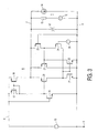
- FIG. 3 shows a somewhat more detailed representation of the feed arrangement 6. Circuit elements already described are again provided with the same reference numerals.
- the power supply via the terminals 4, 5 takes place from a schematically illustrated voltage source 13.
- the equivalent circuit for the data processing circuit 1 is the parallel connection of a current source 14 with the series connection of a resistor 15 and a voltage source 16.
- the food arrangement 6 according to Fig. 3 comprises a first and a second transistor 17, 18, which are connected with their source terminals to the terminal 4.
- the gate terminal of the second transistor 18 is connected to the gate terminal of the first transistor 17 and to its drain terminal.
- the first and second transistors 17, 18 form a current mirror.
- a third transistor 19 has its drain connected to the drain of the first transistor 17 and to a gate of a fourth transistor 20. With its gate terminal, the third transistor 19 is led to the terminal 4. A source terminal of the third transistor 19 is connected to the terminal 5.
- the fourth transistor 20 is connected with its source terminal to the drain terminal of the second transistor 18 and to the supply voltage terminal 2.
- a drain terminal of the fourth transistor 20 is connected to a drain terminal of a sixth transistor 22, to its gate terminal, to a gate terminal of a seventh transistor 23, and to a drain terminal of an eighth transistor 24.
- the sources of the sixth and seventh transistors 22, 23 are connected in common to the terminal 5 so that the sixth and seventh transistors 22, 23 also form a current mirror.
- a fifth transistor 21 is connected with its source terminal to the supply voltage terminal 2, guided with its drain terminal to the terminal 5 and connected with its gate terminal to the drain terminal of the seventh transistor 23.
- a source terminal of the ninth transistor 25 is also connected to the supply voltage terminal 2. While a gate terminal of the ninth transistor 25 is connected directly to the supply voltage terminal 3, the gate terminal of the eighth transistor 24 is fed via a reference source 26 to this supply voltage terminal 3.
- Fig. 4 shows a modification of the embodiment according to Fig. 3 in the out Fig. 3 already known elements are again provided with the same reference numerals.
- a tenth transistor 27 is inserted, whose gate terminal is connected to the gate terminal of the third transistor 19.
- the source-drain path of the tenth transistor 27 is inserted into the connection between the third and the first transistor 19 or 17 such that the drain terminals of the tenth and first transistor 27, 17 with each other and the source terminal of the tenth Transistor 27 is connected to the drain terminal of the third transistor 19 and the gate terminal of the fourth transistor 20.
- a second capacitor 28 is inserted between the gate terminal of the fourth transistor 20 and the terminal 5.
- Fig. 4 Across from Fig. 3 is in Fig. 4 Furthermore, the current mirror of the sixth transistor 22 and the seventh transistor 23 omitted. Accordingly, the drain terminal of the fourth transistor 20 is connected directly to the terminal 5. Also, the drain terminal of the eighth transistor 24 is directly connected to the terminal 5.
- Fig. 5 shows a block diagram of an embodiment of a mobile data carrier according to the invention, which is set up for both contact-based and contactless connections.
- a resonant circuit of an inductor 29 and a third capacitor 30 When supplied at high-frequency electrical energy through the resonant circuit 29, 30, a voltage is generated at this, which is fed via a rectifier 31 to the terminals 4, 5.
- a fourth capacitor 32 which is connected to the terminals 4, 5, serves to screen and smooth the voltage at the terminals 4, 5. Via the current control arrangement 8 and the voltage-limiting control circuit 7, the energy of the data processing circuit 1 is fed to the power supply.
- the disk according to Fig. 5 further comprises a clock conditioning circuit 33 and a data processing circuit 34, to which both via the resonant circuit 29, 30 supplied data or clock signals for separation and signal shaping via a line 35 are supplied.
- the clock conditioning circuit 33 and the data conditioning circuit 34 are also energized from the power supply 6, which is shown in FIG Fig. 5 indicated schematically by the connection 36. Via a clock line 37 or a data line 38, clock signals or data signals are supplied to the data processing circuit 1.
- these data signals are transmitted via a further data line 39 to a modulation device 40 supplied, for example, the resonant circuit 29, 30 influenced by a load modulation.
- the clock line 37 is connected to a first contact 41, the data line 38 to a second contact 42, the further data line 39 to a third contact 43 and the terminal 5 to a fourth contact 44.
- a fifth contact 45 is further provided, which is connected to the terminal 4. In this way, fluctuations of the supply current at the supply voltage terminals 2, 3 do not reach via the fifth contact 45 to the outside of the mobile data carrier. This would be the case if, instead of the fifth contact 45, a sixth contact 46 was provided which is connected directly to the supply voltage terminal 2. Such a sixth contact 46 would allow immediate detections of variations in the supply current to the data processing circuit 1.
Landscapes
- Engineering & Computer Science (AREA)
- Computer Hardware Design (AREA)
- Microelectronics & Electronic Packaging (AREA)
- Physics & Mathematics (AREA)
- General Physics & Mathematics (AREA)
- Theoretical Computer Science (AREA)
- Computer Networks & Wireless Communication (AREA)
- Computer Security & Cryptography (AREA)
- General Engineering & Computer Science (AREA)
- Near-Field Transmission Systems (AREA)
- Power Sources (AREA)
- Credit Cards Or The Like (AREA)
- Storage Device Security (AREA)
- Control Of Electrical Variables (AREA)
Description
- Die Erfindung bezieht sich auf einen mobilen Datenträger, insbesondere eine Chipkarte. Derartige Chipkarten sind auch unter der Bezeichnung Smart Card bekannt geworden.
- Zur Ausforschung von auf derartigen Datenträgem gespeicherten Daten durch Unbefugte ist eine Methode publik gemacht worden, bei der aus dem zeitlichen Verlauf einer Versorgungsspannung an Versorgungsspannungsanschlüssen einer Datenverarbeitungsschaltung innerhalb des Datenträgers sowie aus dem zeitlichen Verlauf eines von der Datenverarbeitungsschaltung an den Versorgungsspannungsanschlüssen aufgenommenen Versorgungsstromes auf in der Datenverarbeitungsschaltung verarbeitete Datenmuster zurückgeschlossen werden können soll.
-
EP 0 874 327 A2 zeigt eine Smart Card mit einer Einrichtung zum Erfassen des Pegels einer durch eine externe Einrichtung bereitgestellten Spannung, wobei ein Aktivierungssignal erzeugt wird, wenn die erfasste Spannung unter einem vorbestimmten Pegel liegt, sowie einer Spannungsregelungseinrichtung, welche die Pegel der bereitgestellten Spannung in Betriebsspannungspegel der Smart Card in Reaktion auf das Aktivierungssignal konvertiert. -
US 5,045,770 zeigt eine Regeleinrichtung zum Empfangen elektrischer Energie aus einem externen magnetischen Wechselfeld mittels eines induktiven Resonanzkreises und zum Ausgeben einer geregelten Ausgangsspannung, deren Ausgangsleistung mittels Abzweigung von Eingangsleistung geregelt wird, wobei getrennte Stromwege für den Abzweigstrom und den Ausgabestrom vorgesehen sind und im Ausgabestromweg eine Gleichrichtereinrichtung vorgesehen ist. -
US 5,495,241 zeigt ein Verfahren und eine Vorrichtung zur Reduzierung von Verlusten in Einrichtungen für kontaktlose Daten- und Energieübertragung, wobei eine Funktionseinheit in einem beweglichen Teil vorgesehen ist, der die aktuellen Verluste in einer Spannungsregelungseinrichtung bestimmt, wobei ein stationärer Teil, wenn ein Sollwert überschritten wird, die Energiezufuhr reduzieren kann. -
US 4,881,199 betrifft eine Leseschaltung für integrierte Logikschaltungen mit einem Speicher, der aus einer Matrix aus Speicherzellen besteht, wobei das Lesen durch Erfassen einer Strom- oder Spannungsänderung erfolgt. - Die Erfindung hat die Aufgabe, bei einem mobilen Datenträger die Ausforschung von Datenmustern durch das vorgenannte Verfahren wenigstens deutlich zu erschweren, wenn nicht unmöglich zu machen.
- Die Aufgabe wird durch einen mobilen Datenträger mit den Merkmalen des Anspruch 1 gelöst. Vorteilhafte Weiterbildungen der Erfindung sind in den sich daran angeschlossenen Unteransprüchen 2 und 3 angegeben.
- Erfindungegemäßen wird diese Aufgabe gelöst durch eine mobilen Datenträger, insbesondere Chipkarte, mit einer Datenverarbeitungsschaltung und einer Speiseanordnung zum Zuführen elektrischer Energie an Versorgungsspannungsanschlüsse zum Betreiben der Datenverarbeitungsschaltung von einer außerhalb des Datenträgers angeordneten, externen Energiequelle, wobei die Speiseanordnung eine spannungsbegrenzende Regelschaltung, die zu den Versorgungsspannungsanschlüssen der Datenverarbeitungsschaltung parallel angeordnet ist, sowie eine Stromsteueranordnung umfasst, die bezüglich der Energiezufuhr zur Datenverarbeitungsschaltung mit der Parallelanordnung der spannungsbegrenzenden Regelschaltung und der Datenverarbeitungsschaltung in Reihe angeordnet ist.
- Durch die Erfindung wird in einfacher und vorteilhafter Weise erreicht, dass von einer außerhalb des Datenträgers angeordneten, externen Energiequelle stets ein konstanter Energiefluss in den Datenträger eingespeist wird. Die Spannung und der Strom, mit denen dieser Energiefluss bewirkt wird, sind an von außerhalb des Datenträgers zugänglichen Schaltungspunkten während des gesamten Betriebes stets konstant und lassen somit keinen Rückschluss auf einzelne Datenverarbeitungsvorgänge innerhalb der Datentverarbeitungsschaltung zu. Insbesondere kann aus dem Energiefluß nicht mehr bitgenau auf die Ausführung einer speziellen Berechnung geschlossen werden.
- Für die erfindungsgemäßen, mobilen Datenträger, insbesondere kontaktlose oder auch kontaktbehaftete Chipkarten, hat die Erfindung die Funktion einer Versorgungsquelle mit den Charakteristiken, daß am empfangenden Ende des Pfades in der Anordnung, über den der Energiefluß zur Datenverarbeitungsschaltung erfolgt, die Last unabhängig von der Last auf der speisenden Seite dieses Pfades ist und daß sich die Quelle an der speisenden Seite über einen weiten Aussteuerungsbereich wie eine Stromquelle verhält. Eine derartige Versorgungsquelle kann durch einen Parallelregler konstruiert werden. Insbesondere weist dabei die kontaktlose Energiespeisung einer Chipkarte die Charakteristik einer Konstantstromquelle auf, ohne dabei geregelt werden zu müssen.
- Eine vorteilhafte Weiterbildung des erfindungsgemäßen, mobilen Datenträgers besteht darin, daß die Stromsteueranordnung zum Liefern eines wenigstens nahezu lastunabhängigen Speisestroms eingerichtet ist und daß die spannungsbegrenzende Regelschaltung zur Aufnahme eines Überschußstromes ausgebildet ist, der bezüglich des Speisestromes zu einem von der Datenverarbeitungsschaltung an den Versorgungsspannungsanschlüssen aufgenommenen Versorgungsstrom komplementär ist.
- Nach einer weiteren, vorteilhaften Ausgestaltung ist der erfindungsgemäße, mobile Datenträger dadurch gekennzeichnet, daß der von der Stromsteueranordnung gelieferte Speisestrom wenigstens nahezu nur von einer von der externen Energiequelle abgegebenen Spannung abhängig gesteuert ist.
- Eine weitere Angriffsmöglichkeit bietet sich bei dem eingangs genannten Ausforschungsverfahren bei einem mobilen Datenträger dadurch, daß in einer Datenverarbeitungsschaltung im Datenträger synchron getaktete Logikelemente eingesetzt sind, die mit Hilfe eines synchronen Taktsignals zeitlich streng geordnet steuerbar sind. Diese zeitliche Steuerung erleichtert die Zuordnung von Bitmustern zu Datenverarbeitungsvorgängen bei einem unberechtigten Zugriff.
- Nach einer bevorzugten Weiterbildung ist der erfindungsgemäße, mobile Datenträger dadurch gekennzeichnet, daß die Datenverarbeitungsschaltung mit asynchron arbeitenden Logikelementen ausgebildet ist, deren Signalverarbeitungsgeschwindigkeit von einer an den Versorgungsspannungsanschlüssen der Datenverarbeitungsschaltung angelegten Versorgungsspannung abhängig ist.
- Durch Einsatz asynchron arbeitender Logikelemente in der Datenverarbeitungsschaltung des erfindungsgemäßen, mobilen Datenträgers kann eine Verwirrung beim unberechtigten Zugriff erreicht werden. Schaltvorgänge, die durch derartige, asynchron arbeitende Logikelemente auf die Versorgungsspannungsanschlüsse der Datenverarbeitungsschaltung übertragen werden, erzeugen dort ein unkorrelierbares Muster, aus dem nicht auf verarbeitete Datenmuster rückgeschlossen werden kann. Vorteilhaft ist dabei die Signalverarbeitungsgeschwindigkeit der Logikelemente von der Versorgungsspannung abhängig. Der Datendurchsatz der Datenverarbeitungsschaltung wird somit selbsttätig der verfügbaren Versorgungsspannung angepaßt. Eine derart ausgebildete Datenverarbeitungsschaltung ist über einen weiten Versorgungsspannungsbereich funktionsfähig bei vergleichsweise geringem Schaltungsaufwand.
- In dieser Ausgestaltung weist der erfindungsgemäße, mobile Datenträger den weiteren Vorteil auf, daß keine Interferenz von Signalen aus der Datentverarbeitungsschaltung mit Signalen erfolgt, die dem mobilen Datenträger von außerhalb zugeführt werden oder die der mobile Datenträger nach außerhalb abgibt. Der Schutz gegen das eingangs genannte Ausforschungsverfahren ist besonders hoch, da nicht einmal die elektromagnetische Abstrahlung der Datenverarbeitungsschaltung im mobilen Datenträger Informationen über Datenmuster in der Datenverarbeitungsschaltung enthält. Der vom mobilen Datenträger aufgenommene Speisestrom ist von den verarbeiteten Datenmustern unabhängig. Je nach Leistungsfähigkeit der Energiezufuhr zum mobilen Datenträger wird die Verarbeitungsgeschwindigkeit in der Datenverarbeitungsschaltung stets auf den optimal möglichen Wert eingestellt. Gegenüber einer Ausbildung der Datenverarbeitungsschaltung mit synchron getakteten Logikelementen kann insbesondere ein wesentlich kleiner dimensionierter Filterkondensator zur Störunterdrückung eingesetzt werden. Bezüglich der Ausforschung von Datenmustern in der Datenverarbeitungsschaltung wird insbesondere eine Verschleierung der Zeitbereiche erzielt, in denen die Dateneingabe, Datenausgabe und Berechnungen durchgeführt werden. Es kann erreicht werden, daß von außen nicht mehr möglich ist, festzustellen, wann ein wirklicher Rechenvorgang oder eine Eingabe oder Ausgabe stattfindet.
- Ausführungsbeispiele der Erfindung sind in der Zeichnung dargestellt und werden im nachfolgenden näher beschrieben. Es zeigen
-
Fig. 1 blockschematisch ein erstes Ausführungsbeispiel, -
Fig. 2 blockschematisch ein zweites Ausführungsbeispiel, -
Fig. 3 eine detailliertere Darstellung eines dritten Ausführungsbeispiels, -
Fig. 4 eine detailliertere Darstellung eines vierten Ausführungsbeispiels und -
Fig. 5 eine blockschematische Darstellung eines erfindungsgemäßen, mobilen Datenträgers. - Die Anordnung nach
Fig. 1 umfaßt eine Datentverarbeitungsschaltung 1 mit zwei Versorgungsspannungsanschlüssen 2, 3. Über diese wird der Datenverarbeitungsschaltung 1 eine Versorgungsspannung zugeleitet, die der Energiezufuhr zur Datenverarbeitungsschaltung 1 dient. Von einer externen, außerhalb des Datenträgers angeordneten und inFig.1 nicht dargestellten Energiequelle wird elektrische Energie über zwei Anschlüsse 4, 5 zugeführt. Beispielsweise sind die Anschlüsse 4, 5 mit einer Schaltungsanordnung verbunden, die bei einer kontaktlosen Chipkarte eine übertragene elektrische Spannung gleichrichtet und diese gleichgerichtete Spannung zur Energieversorgung der Datenverarbeitungsschaltung 1 zur Verfügung stellt. - Die Anschlüsse 4, 5 bilden Eingänge einer Speiseanordnung 6, die eine spannungsbegrenzende Regelschaltung 7 und eine Stromsteueranordnung 8 umfaßt. Die spannungsbegrenzende Regelschaltung 7 ist zu den Versorgungsspannungsanschlüssen 2, 3 parallel angeordnet. Die Stromsteueranordnung 8 ist zu der Parallelschaltung der spannungsbegrenzenden Regelschaltung 7 und der Datenverarbeitungsschaltung 1 in Reihe angeordnet. Diese Reihenanordnung ist zwischen den Anschlüssen 4 und 5 angeordnet. Die Stromsteueranordnung 8 ist zum Liefern eines wenigstens nahezu lastunabhängigen Speisestroms eingerichet, der in
Fig. 1 durch den Pfeil mit dem Bezugszeichen 9 angedeutet ist. Wenigstens in einem bestimmten Aussteuerungsbereich weist die Stromsteueranordnung 8 somit das Verhalten einer wenigstens nahezu idealen Stromquelle auf. Der Speisestrom 9 kann allenfalls durch eine zwischen den Anschlüssen 4 und 5 anliegende Spannung gesteuert werden, um die Energiezufuhr zur Datenverarbeitungsschaltung 1 dieser Spannung zwischen den Anschlüssen 4 und 5 anzupassen. - Die Datenverarbeitungsschaltung 1 ist bevorzugt mit asynchronen Logikelementen ausgebildet, deren Signalverarbeitungsgeschwindigkeit von dem zur Verfügung stehenden Speisestrom 9 als maximalem Versorgungsstrom an den Versorgungsspannungsanschlüssen 2, 3 abhängig ist. Je nach in der Datenverarbeitungsschaltung I vorgenommenen Operationen wird jedoch der Versorgungsstrom, in
Fig. 1 mit dem Pfeil 10 bezeichnet, geringer sein als der Speisestrom 9. Ein Überschußstrom, dargestellt durch den Pfeil 11 inFig. 1 , der bezüglich des Speisestromes 9 zu dem Versorgungsstrom 10 komplementär ist, fließt durch die spannungsbegrenzende Regelschaltung 7 ab. Dadurch kann der Speisestrom 9 datenunabhängig bemessen werden. Parallel zu den Versorgungspannungsanschlüssen 2, 3 ist außerdem ein Kondensator 12 angeordnet, der insbesondere bei kontaktlosen Chipkarten zur Vermeidung von Interferenzen zwischen Signalen in der Datenverarbeitungsschaltung 1 und Signalen dient, die von der Chipkarte von außerhalb empfangen oder nach außerhalb übertragen werden. Bei der erfindungsgemäßen Ausbildung des mobilen Datenträgers kann dieser Kondensator 12 sehr klein dimensioniert werden. - Die spannungsbegrenzende Regelschaltung 7 hat neben der Aufnahme des Überschußstromes 11 die Funktion, die Versorgungsspannung an den Versorgungsspannungsanschlüssen 2, 3 innerhalb eines vorgegebenen Spannungsbereichs zu halten. Der Kondensator 12 dient außerdem zur Mittlung, d.h. zum Ausgleich von Lastspitzen in der Datenverarbeitungsschaltung 1. Da diese durch Verwendung asynchroner Logikelemente bereits stark vermindert werden können, ist auch hierfür nur ein kleiner Kondensator erforderlich.
- Mit dem Aufbau gemäß
Fig. 1 kann zur Ausregelung von datenabhängigen Versorgungsströmen auf eine Regelschleife verzichtet werden, die stets eine endliche Regelgeschwindigkeit aufweist und damit konstruktionsbedingt keine vollständige Unterdrückung derartiger Datenabhängigkeiten in der Energiezufuhr bewirken kann. Beim erfindungsgemäßen, mobilen Datenträger ist der Speisestrom 9 vollständig konstant ohne Datenabhängigkeit. Durch die spannungsbegrenzende Wirkungsweise der Regelschaltung 7 wird erreicht, daß die Stromsteueranordnung 8 auch bei schwankenden Versorgungsströmen 10 in ihrem Regelbereich bleibt und somit der Speisestrom 9 konstant gehalten werden kann. - Durch die Steuerung der Stromsteueranordnung 8 nach der Spannung an den Anschlüssen 4, 5 kann der Speisestrom 9 an die Versorgungsstrom-VersorgungsspannungsCharakteristik der Datentverarbeitungsschaltung 1 angepaßt werden.
-
Fig. 2 zeigt eine vereinfachte, blockschematische Darstellung, in der mitFig. 1 übereinstimmende Elemente mit denselben Bezugszeichen versehen sind. Die spannungsbegrenzende Regelschaltung 7 wird hier durch eine Zenerdiode dargestellt, und die Stromsteueranordnung 8 ist durch eine ideale Stromquelle wiedergegeben. Diese Stromquelle ist als ungeregelte Stromquelle, d.h. nicht einstellbar, dargestellt. Durch die Zenerdiode 7 wird die Versorgungsspannung für die Datenverarbeitungsschaltung 1 in einem weiten Bereich der Energiezufuhr über die Anschlüsse 4, 5 sowie der Signalverarbeitungsvorgänge in der Datenverarbeitungsschaltung 1 konstant gehalten. - Das Ausführungsbeispiel nach
Fig. 3 zeigt eine etwas detailliertere Darstellung der Speiseanordnung 6. Bereits beschriebene Schaltungselemente sind wieder mit denselben Bezugszeichen versehen. Die Energiezufuhr über die Anschlüsse 4, 5 erfolgt aus einer schematisch dargestellten Spannungsquelle 13. Als Ersatzschaltbild für die Datenverarbeitungsschaltung 1 dient die Parallelschaltung einer Stromquelle 14 mit der Reihenschaltung aus einem Widerstand 15 und einer Spannungsquelle 16. - Die Speiseanordnung 6 gemäß
Fig. 3 umfaßt einen ersten und einen zweiten Transistor 17, 18, die mit ihren Source-Anschlüssen mit dem Anschluß 4 verbunden sind. Der Gate-Anschluß des zweiten Transistors 18 ist mit dem Gate-Anschluß des ersten Transistors 17 und mit dessen Drain-Anschluß verbunden. Der erste und der zweite Transistor 17, 18 bilden einen Stromspiegel. - Ein dritter Transistor 19 ist mit seinem Drain-Anschluß an den Drain-Anschluß des ersten Transistors 17 und an einen Gate-Anschluß eines vierten Transistors 20 angeschlossen. Mit seinem Gate-Anschluß ist der dritte Transistor 19 an den Anschluß 4 geführt. Ein Source-Anschluß des dritten Transistors 19 ist mit dem Anschluß 5 verbunden.
- Der vierte Transistor 20 ist mit seinem Source-Anschluß an den Drain-Anschluß des zweiten Transistors 18 und an den Versorgungsspannungsanschluß 2 angeschlossen. Ein Drain-Anschluß des vierten Transistors 20 ist mit einem Drain-Anschluß eines sechsten Transistors 22, mit dessen Gate-Anschluß, mit einem Gate-Anschluß eines siebten Transistors 23und mit einem Drain-Anschluß eines achten Transistors 24 verbunden. Die Source-Anschlüsse des sechsten und siebten Transistors 22, 23 sind gemeinsam mit dem Anschluß 5 verbunden, so daß der sechste und der siebte Transistor 22, 23 ebenfalls einen Stromspiegel bilden. Ein fünfter Transistor 21 ist mit seinem Source-Anschluß an den Versorgungsspanungsanschluß 2 angeschlossen, mit seinem Drain-Anschluß an den Anschluß 5 geführt und mit seinem Gate-Anschluß mit dem Drain-Anschluß des siebten Transistors 23 verbunden. Außerdem besteht eine Verbindung zwischen dem Gate-Anschluß des fünften Transistors 21 und dem Source-Anschluß des achten Transistors 24 sowie dem Drain-Anschluß eines neunten Transistors 25. Ein Source-Anschluß des neunten Transistors 25 ist ebenfalls mit dem Versorgungsspannungsanschluß 2 verbunden. Während ein Gate-Anschluß des neunten Transistors 25 mit dem Versorgungsspannungsanschluß 3 unmittelbar verbunden ist, ist der Gate-Anschluß des achten Transistos 24 über eine Referenzquelle 26 an diesen Versorgungsspannungsanschluß 3 geführt.
-
Fig. 4 zeigt eine Abwandlung des Ausführungsbeispiels nachFig. 3 , in der ausFig. 3 bereits bekannte Elemente wieder mit denselben Bezugszeichen versehen sind. GegenüberFig. 3 ist in der Schaltung nachFig. 4 ein zehnter Transistor 27 eingefügt, dessen Gate-Anschluß mit dem Gate-Anschluß des dritten Transistors 19 verbunden ist. Die Source-Drain-Strecke des zehnten Transistors 27 ist in die Verbindung zwischen dem dritten und dem ersten Transistor 19 bzw. 17 derart eingefügt, daß die Drain-Anschlüsse des zehnten und es ersten Transistors 27, 17 miteinander und der Source-Anschluß des zehnten Transistors 27 mit dem Drain-Anschluß des dritten Transistors 19 sowie dem Gate-Anschluß des vierten Transistors 20 verbunden ist. Ein zweiter Kondensator 28 ist zwischen dem Gate-Anschluß des vierten Transistors 20 und dem Anschluß 5 eingefügt. - Gegenüber
Fig. 3 ist inFig. 4 ferner der Stromspiegel aus dem sechsten Transistor 22 und dem siebten Transistor 23 entfallen. Demzufolge ist der Drain-Anschluß des vierten Transistors 20 unmittelbar an den Anschluß 5 angeschlossen. Auch der Drain-Anschluß des achten Transistors 24 ist unmittelbar mit dem Anschluß 5 verbunden. -
Fig. 5 zeigt blockschematisch ein Ausführungsbeispiel eines erfindungsgemäßen, mobilen Datenträgers, der sowohl für kontaktbehaftete als auch für kontaktlose Verbindungen eingerichtet ist. Mit Elementen aus den vorbeschriebenen Figuren übereinstimmende Elemente sind wieder mit denselben Bezugszeichen versehen. - Zur kontaktlosen Energiezufuhr und Datenübertragung enthält der Datenträger gemäß
Fig. 5 einen Resonanzkreis aus einer Induktivität 29 und einem dritten Kondensator 30. Bei Zufuhr bei hochfrequenter elektrischer Energie über den Resonanzkreis 29, 30 wird an diesem eine Spannung erzeugt, die über eine Gleichrichteranordnung 31 den Anschlüssen 4, 5 zugeleitet wird. Ein vierter Kondensator 32, der mit den Anschlüssen 4, 5 verbunden ist, dient der Siebung und Glättung der Spannung an den Anschlüssen 4, 5. Über die Stromsteueranordnung 8 und die spannungsbegrenzende Regelschaltung 7 wird die Energie der Datenverarbeitungsschaltung 1 zur Speisung zugeleitet. - Der Datenträger gemäß
Fig. 5 umfaßt weiterhin eine Taktaufbereitungsschaltung 33 sowie eine Datenaufbereitungsschaltung 34, denen beiden über den Resonanzkreis 29, 30 zugeführte Daten- bzw. Taktsignale zur Trennung und Signalformung über eine Leitung 35 zugeführt werden. Die Taktaufbereitungsschaltung 33 und die Datenaufbereitungsschaltung 34 werden außerdem ebenfalls aus der Speiseanordnung 6 mit Energie versorgt, was inFig. 5 durch die Verbindung 36 schematisch angedeutet ist. Über eine Taktleitung 37 bzw. eine Datenleitung 38 werden Taktsignale bzw. Datensignale der Datenverarbeitungsschaltung 1 zugeführt. - Zur Abgabe von Datensignalen von der Datenverarbeitungsschaltung 1 werden diese Datensignale über eine weitere Datenleitung 39 einer Modulationseinrichtung 40 zugeführt, die beispielsweise den Resonanzkreis 29, 30 über eine Belastungsmodulation beeinflußt.
- Zur kontaktbehafteten Verbindung des mobilen Datenträgers gemäß
Fig. 5 mit externen Anordnungen zur Datenübertragung und Energiezufuhr sind die Taktleitung 37 mit einem ersten Kontakt 41, die Datenleitung 38 mit einem zweiten Kontakt 42, die weitere Datenleitung 39 mit einem dritten Kontakt 43 und der Anschluß 5 mit einem vierten Kontakt 44 verbunden. Zur Energiezufuhr ist weiterhin ein fünfter Kontakt 45 vorgesehen, der an den Anschluß 4 angeschlossen ist. Auf diese Weise gelangen Schwankungen des Versorgungsstromes an den Versorgungsspannungsanschlüssen 2, 3 nicht über den fünften Kontakt 45 nach außerhalb des mobilen Datenträgers. Dieses wäre der Fall, wenn anstelle des fünften Kontaktes 45 ein sechster Kontakt 46 vorgesehen wäre, der unmittelbar mit dem Versorgungsspannungsanschluß 2 verbunden ist. Über einen solchen sechsten Kontakt 46 wären unmittelbare Detektionen von Schwankungen des Versorgungsstromes für die Datenverarbeitungsschaltung 1 möglich.
Claims (3)
- Mobiler Datenträger, insbesondere Chipkarte, mit einer Datenverarbeitungsschaltung (1) und einer Speiseanordnung (6) zum Zuführten elektrischer Energie an Versorgungsspannungsanschlüsse (2, 3) zum Betreiben der Datenverarbeitungsschaltung (1) von einer außerhalb des Datenträgers angeordneten, externen Energiequelle,
wobei die Speiseanordnung (6) eine spannungsbegrenzende Regelschaltung (7), die zu den Versorgungsspannungsanschlüssen (2, 3) der Datenverarbeitungsschaltung (1) parallel angeordnet ist, umfasst,
dadurch gekennzeichnet,
dass die Speiseanordnung (6) weiter eine Stromsteueranordnung (8) umfasst, die bezüglich der Energiezufuhr zur Datenverarbeitungsschaltung (1) mit der Parallelanordnung der spannungsbegrenzenden Regelschaltung (7) und der Datenverarbeitungsschaltung (1) in Reihe angeordnet ist,
dass die Stromsteueranordnung (8) zum Liefern eines wenigstens nahezu lastunabhängigen Speisestroms (9) eingerichtet ist, und
dass die spannungsbegrenzende Regelschaltung (7) zur Aufnahme eines Überschussstromes (11) ausgebildet ist, der bezüglich des Speisestromes (9) zu einem von der Datenverarbeitungsschaltung (1) an den Versorgungsspannungsanschlüssen (2, 3) aufgenommenen Versorgungsstrom (10) komplementär ist. - Mobiler Datenträger nach Anspruch 1, dadurch gekennzeichnet,
dass der von der Stromsteueranordnung (8) gelieferte Speisestrom (9) wenigstens nahezu nur von einer von der externen Energiequelle abgegebenen Spannung abhängig gesteuert ist. - Mobiler Datenträger nach Anspruch 1 oder 2, dadurch gekennzeichnet,
dass die Datenverarbeitungsschaltung (1) mit asynchron arbeitenden Logikelementen ausgebildet ist, deren Signalverarbeitungsgeschwindigkeit von einer an den Versorgungsspannungsanschlüssen (2, 3) der Datenverarbeitungsschaltung (1) angelegten Versorgungsspannung abhängig ist.
Priority Applications (1)
| Application Number | Priority Date | Filing Date | Title |
|---|---|---|---|
| EP99965561.6A EP1062632B1 (de) | 1999-01-07 | 1999-12-24 | Mobiler datenträger |
Applications Claiming Priority (6)
| Application Number | Priority Date | Filing Date | Title |
|---|---|---|---|
| DE19900261 | 1999-01-07 | ||
| DE19900261 | 1999-01-07 | ||
| EP99100168 | 1999-01-07 | ||
| EP99100168 | 1999-01-07 | ||
| EP99965561.6A EP1062632B1 (de) | 1999-01-07 | 1999-12-24 | Mobiler datenträger |
| PCT/EP1999/010405 WO2000041130A1 (de) | 1999-01-07 | 1999-12-24 | Mobiler datenträger |
Publications (2)
| Publication Number | Publication Date |
|---|---|
| EP1062632A1 EP1062632A1 (de) | 2000-12-27 |
| EP1062632B1 true EP1062632B1 (de) | 2015-05-20 |
Family
ID=26051220
Family Applications (1)
| Application Number | Title | Priority Date | Filing Date |
|---|---|---|---|
| EP99965561.6A Expired - Lifetime EP1062632B1 (de) | 1999-01-07 | 1999-12-24 | Mobiler datenträger |
Country Status (5)
| Country | Link |
|---|---|
| US (1) | US6996726B1 (de) |
| EP (1) | EP1062632B1 (de) |
| JP (1) | JP2002534749A (de) |
| KR (1) | KR100697489B1 (de) |
| WO (1) | WO2000041130A1 (de) |
Families Citing this family (9)
| Publication number | Priority date | Publication date | Assignee | Title |
|---|---|---|---|---|
| CN1287325C (zh) * | 2001-08-08 | 2006-11-29 | 皇家飞利浦电子股份有限公司 | 带有有源信号处理电路和无源信号处理电路的数据载体 |
| US7113547B2 (en) * | 2001-08-24 | 2006-09-26 | Matsushita Electric Industrial Co., Ltd. | Data communication system, controller device and data communication method |
| KR100528464B1 (ko) * | 2003-02-06 | 2005-11-15 | 삼성전자주식회사 | 스마트카드의 보안장치 |
| JP4455079B2 (ja) | 2004-01-30 | 2010-04-21 | 富士通マイクロエレクトロニクス株式会社 | 電源回路 |
| DE102004014203B4 (de) * | 2004-03-23 | 2006-02-02 | Infineon Technologies Ag | Kontaktloser Datenträger mit Stromdemodulation |
| DE102005005812A1 (de) * | 2005-02-09 | 2006-08-17 | Atmel Germany Gmbh | Schaltungsanordnung und Verfahren zur Spannungsversorgung eines Transponders |
| US7538673B2 (en) * | 2005-08-26 | 2009-05-26 | Texas Instruments Incorporated | Voltage regulation circuit for RFID systems |
| KR102068653B1 (ko) | 2013-03-13 | 2020-01-21 | 삼성전자주식회사 | 비접촉 ic 카드의 내부 전압 생성기 및 이를 포함하는 비접촉 ic 카드 |
| EP4560525A1 (de) * | 2023-11-24 | 2025-05-28 | EM Microelectronic-Marin SA | Gleichrichterschaltung für ein rfid-etikett |
Family Cites Families (15)
| Publication number | Priority date | Publication date | Assignee | Title |
|---|---|---|---|---|
| FR2609831B1 (fr) * | 1987-01-16 | 1989-03-31 | Thomson Semiconducteurs | Circuit de lecture pour memoire |
| ZA89871B (en) * | 1988-02-04 | 1990-10-31 | Magelian Corp Aust Pty Ltd | Shunt regulator |
| US5247164A (en) * | 1989-01-26 | 1993-09-21 | Hitachi Maxell, Ltd. | IC card and portable terminal |
| US5495241A (en) * | 1991-01-25 | 1996-02-27 | Siemens Aktiengesellschaft | Method for reducing power loss in devices for contactless data and energy transfer, and apparatus for performing the method |
| JPH0528330A (ja) * | 1991-07-24 | 1993-02-05 | Mitsubishi Electric Corp | 非接触型可搬担体及びその初期化方法 |
| DE69228473T3 (de) * | 1991-12-04 | 2002-07-11 | Citizen Watch Co., Ltd. | Datenträger |
| JPH087059A (ja) * | 1994-06-21 | 1996-01-12 | Sony Chem Corp | 非接触情報カード |
| JP3493096B2 (ja) * | 1996-06-07 | 2004-02-03 | 株式会社東芝 | 半導体集積回路、icカード、及びicカードシステム |
| SG54559A1 (en) * | 1996-09-13 | 1998-11-16 | Hitachi Ltd | Power transmission system ic card and information communication system using ic card |
| US6027029A (en) * | 1997-04-21 | 2000-02-22 | Samsung Electronics Co., Ltd | Smart card capable of adjusting voltages supplied from external device |
| US6173899B1 (en) * | 1998-04-03 | 2001-01-16 | Alexander Rozin | Method and system for contactless energy transmission and data exchange between a terminal and IC card |
| US5998978A (en) * | 1998-06-29 | 1999-12-07 | Motorola, Inc. | Apparatus and method for reducing energy fluctuations in a portable data device |
| US6118306A (en) * | 1998-12-03 | 2000-09-12 | Intel Corporation | Changing clock frequency |
| US6134130A (en) * | 1999-07-19 | 2000-10-17 | Motorola, Inc. | Power reception circuits for a device receiving an AC power signal |
| US6507913B1 (en) * | 1999-12-30 | 2003-01-14 | Yeda Research And Development Co. Ltd. | Protecting smart cards from power analysis with detachable power supplies |
-
1999
- 1999-12-24 EP EP99965561.6A patent/EP1062632B1/de not_active Expired - Lifetime
- 1999-12-24 WO PCT/EP1999/010405 patent/WO2000041130A1/de not_active Ceased
- 1999-12-24 US US09/623,643 patent/US6996726B1/en not_active Expired - Lifetime
- 1999-12-24 JP JP2000592787A patent/JP2002534749A/ja active Pending
- 1999-12-24 KR KR1020007009880A patent/KR100697489B1/ko not_active Expired - Lifetime
Also Published As
| Publication number | Publication date |
|---|---|
| JP2002534749A (ja) | 2002-10-15 |
| WO2000041130A1 (de) | 2000-07-13 |
| US6996726B1 (en) | 2006-02-07 |
| KR100697489B1 (ko) | 2007-03-20 |
| KR20010085222A (ko) | 2001-09-07 |
| EP1062632A1 (de) | 2000-12-27 |
Similar Documents
| Publication | Publication Date | Title |
|---|---|---|
| DE69801926T2 (de) | Kontaktchipkarte/kontaktlose chipkarte mit abänderungsfähiger antennenschnittstelle | |
| DE69933520T2 (de) | Datenträger mit korrekturmöglichkeiten und verbesserter spannungsbegrenzungsmöglichkeit | |
| EP0583690B1 (de) | Chip-Karte mit Feldstärkedetektor | |
| DE102004013177B4 (de) | Datenübertragungseinheit mit einer Datenübertragungsschnittstelle und ein Verfahren zum Betreiben der Datenübertragungseinheit | |
| DE60225093T2 (de) | Einschalt-Rücksetzschaltung für eine Chipkarte | |
| EP0846307B1 (de) | Chipkarte | |
| DE69705595T2 (de) | Kontaktloses Informations-Speichermedium und Verfahren zur Datenübertragung dazu | |
| DE68925029T2 (de) | Shuntregelvorrichtung. | |
| DE60120703T2 (de) | Passiver transponder mit niedrigem energieverbrauch | |
| DE60037989T2 (de) | Transponder für unterschiedliche Einsatzzwecke | |
| EP2132721B1 (de) | Vorrichtung zum ansteuern eines aktuators | |
| DE69232627T2 (de) | Verfahren zur kontaktfreien Kommunikation zwischen einem Halbleiter- Datenaufzeichnungsträger und einer Lese-/Schreibvorrichtung | |
| DE112009003513B4 (de) | Nahfeld-HF-Kommunikationsgeräte | |
| DE4104274C2 (de) | Verfahren zur Regelung der Versorgungsspannung für eine Last | |
| WO1997029454A1 (de) | Vorrichtung zum verarbeiten und speichern von daten | |
| DE102008058760A1 (de) | Schaltung und Verfahren zum Gleichrichten und Regeln von Spannungen | |
| DE10259384B3 (de) | Vorrichtung zur Ermittlung des Energiezustandes eines Energiespeichers eines mobilen Datenträgers | |
| DE102016105875A1 (de) | Gleichrichterschaltkreis, Energiequellschaltkreis und RFID Tag | |
| DE69913142T2 (de) | Vorrichtung und verfahren zur sicheren informationsverarbeitung | |
| DE69230088T2 (de) | Lese/Schreibsystem für Aufzeichnungsmedium und kontaktfreies IC-Karten-System | |
| WO2000041130A1 (de) | Mobiler datenträger | |
| DE102006048594B4 (de) | Schaltungsanordnung zum kontaktlosen Datenaustausch und Chipkarte | |
| EP0953936A1 (de) | Datenträger sowohl für den kontaktlosen als auch den kontaktbehafteten Betrieb | |
| DE69703693T2 (de) | Integrierte Schaltung mit einem eine durch einen programmierbaren Schalter einstellbare Kapazität aufweisenden Resonanzkreis | |
| EP1101192B1 (de) | Datenträger mit regelung der leistungsaufnahme |
Legal Events
| Date | Code | Title | Description |
|---|---|---|---|
| PUAI | Public reference made under article 153(3) epc to a published international application that has entered the european phase |
Free format text: ORIGINAL CODE: 0009012 |
|
| AK | Designated contracting states |
Kind code of ref document: A1 Designated state(s): AT BE CH CY DE DK ES FI FR GB GR IE IT LI LU MC NL PT SE |
|
| 17P | Request for examination filed |
Effective date: 20010115 |
|
| RAP1 | Party data changed (applicant data changed or rights of an application transferred) |
Owner name: PHILIPS CORPORATE INTELLECTUAL PROPERTY GMBH Owner name: KONINKLIJKE PHILIPS ELECTRONICS N.V. |
|
| RAP1 | Party data changed (applicant data changed or rights of an application transferred) |
Owner name: PHILIPS INTELLECTUAL PROPERTY & STANDARDS GMBH Owner name: KONINKLIJKE PHILIPS ELECTRONICS N.V. |
|
| RBV | Designated contracting states (corrected) |
Designated state(s): AT DE FR GB |
|
| RAP1 | Party data changed (applicant data changed or rights of an application transferred) |
Owner name: PHILIPS INTELLECTUAL PROPERTY & STANDARDS GMBH Owner name: NXP B.V. |
|
| RAP1 | Party data changed (applicant data changed or rights of an application transferred) |
Owner name: NXP B.V. |
|
| 17Q | First examination report despatched |
Effective date: 20091021 |
|
| GRAP | Despatch of communication of intention to grant a patent |
Free format text: ORIGINAL CODE: EPIDOSNIGR1 |
|
| INTG | Intention to grant announced |
Effective date: 20150108 |
|
| GRAS | Grant fee paid |
Free format text: ORIGINAL CODE: EPIDOSNIGR3 |
|
| GRAA | (expected) grant |
Free format text: ORIGINAL CODE: 0009210 |
|
| AK | Designated contracting states |
Kind code of ref document: B1 Designated state(s): AT DE FR GB |
|
| REG | Reference to a national code |
Ref country code: GB Ref legal event code: FG4D Free format text: NOT ENGLISH |
|
| REG | Reference to a national code |
Ref country code: AT Ref legal event code: REF Ref document number: 728058 Country of ref document: AT Kind code of ref document: T Effective date: 20150615 |
|
| REG | Reference to a national code |
Ref country code: DE Ref legal event code: R096 Ref document number: 59915428 Country of ref document: DE Effective date: 20150625 |
|
| REG | Reference to a national code |
Ref country code: FR Ref legal event code: PLFP Year of fee payment: 17 |
|
| REG | Reference to a national code |
Ref country code: DE Ref legal event code: R097 Ref document number: 59915428 Country of ref document: DE |
|
| PLBE | No opposition filed within time limit |
Free format text: ORIGINAL CODE: 0009261 |
|
| 26N | No opposition filed |
Effective date: 20160223 |
|
| REG | Reference to a national code |
Ref country code: FR Ref legal event code: PLFP Year of fee payment: 18 |
|
| REG | Reference to a national code |
Ref country code: AT Ref legal event code: MM01 Ref document number: 728058 Country of ref document: AT Kind code of ref document: T Effective date: 20151224 |
|
| PG25 | Lapsed in a contracting state [announced via postgrant information from national office to epo] |
Ref country code: AT Free format text: LAPSE BECAUSE OF NON-PAYMENT OF DUE FEES Effective date: 20151224 |
|
| REG | Reference to a national code |
Ref country code: FR Ref legal event code: PLFP Year of fee payment: 19 |
|
| PGFP | Annual fee paid to national office [announced via postgrant information from national office to epo] |
Ref country code: DE Payment date: 20181126 Year of fee payment: 20 |
|
| PGFP | Annual fee paid to national office [announced via postgrant information from national office to epo] |
Ref country code: FR Payment date: 20181127 Year of fee payment: 20 Ref country code: GB Payment date: 20181127 Year of fee payment: 20 |
|
| REG | Reference to a national code |
Ref country code: DE Ref legal event code: R071 Ref document number: 59915428 Country of ref document: DE |
|
| REG | Reference to a national code |
Ref country code: GB Ref legal event code: PE20 Expiry date: 20191223 |
|
| PG25 | Lapsed in a contracting state [announced via postgrant information from national office to epo] |
Ref country code: GB Free format text: LAPSE BECAUSE OF EXPIRATION OF PROTECTION Effective date: 20191223 |