EP1061663A1 - Procede permettant d'identifier des etiquettes chevauchantes - Google Patents
Procede permettant d'identifier des etiquettes chevauchantes Download PDFInfo
- Publication number
- EP1061663A1 EP1061663A1 EP99954393A EP99954393A EP1061663A1 EP 1061663 A1 EP1061663 A1 EP 1061663A1 EP 99954393 A EP99954393 A EP 99954393A EP 99954393 A EP99954393 A EP 99954393A EP 1061663 A1 EP1061663 A1 EP 1061663A1
- Authority
- EP
- European Patent Office
- Prior art keywords
- tag
- antenna coil
- resonance
- overlapped
- tags
- Prior art date
- Legal status (The legal status is an assumption and is not a legal conclusion. Google has not performed a legal analysis and makes no representation as to the accuracy of the status listed.)
- Withdrawn
Links
Images


Classifications
-
- G—PHYSICS
- G06—COMPUTING OR CALCULATING; COUNTING
- G06K—GRAPHICAL DATA READING; PRESENTATION OF DATA; RECORD CARRIERS; HANDLING RECORD CARRIERS
- G06K19/00—Record carriers for use with machines and with at least a part designed to carry digital markings
- G06K19/06—Record carriers for use with machines and with at least a part designed to carry digital markings characterised by the kind of the digital marking, e.g. shape, nature, code
- G06K19/067—Record carriers with conductive marks, printed circuits or semiconductor circuit elements, e.g. credit or identity cards also with resonating or responding marks without active components
- G06K19/07—Record carriers with conductive marks, printed circuits or semiconductor circuit elements, e.g. credit or identity cards also with resonating or responding marks without active components with integrated circuit chips
- G06K19/077—Constructional details, e.g. mounting of circuits in the carrier
- G06K19/07749—Constructional details, e.g. mounting of circuits in the carrier the record carrier being capable of non-contact communication, e.g. constructional details of the antenna of a non-contact smart card
- G06K19/07773—Antenna details
- G06K19/07777—Antenna details the antenna being of the inductive type
- G06K19/07779—Antenna details the antenna being of the inductive type the inductive antenna being a coil
-
- G—PHYSICS
- G06—COMPUTING OR CALCULATING; COUNTING
- G06K—GRAPHICAL DATA READING; PRESENTATION OF DATA; RECORD CARRIERS; HANDLING RECORD CARRIERS
- G06K19/00—Record carriers for use with machines and with at least a part designed to carry digital markings
- G06K19/06—Record carriers for use with machines and with at least a part designed to carry digital markings characterised by the kind of the digital marking, e.g. shape, nature, code
- G06K19/067—Record carriers with conductive marks, printed circuits or semiconductor circuit elements, e.g. credit or identity cards also with resonating or responding marks without active components
- G06K19/07—Record carriers with conductive marks, printed circuits or semiconductor circuit elements, e.g. credit or identity cards also with resonating or responding marks without active components with integrated circuit chips
- G06K19/0701—Record carriers with conductive marks, printed circuits or semiconductor circuit elements, e.g. credit or identity cards also with resonating or responding marks without active components with integrated circuit chips at least one of the integrated circuit chips comprising an arrangement for power management
-
- G—PHYSICS
- G06—COMPUTING OR CALCULATING; COUNTING
- G06K—GRAPHICAL DATA READING; PRESENTATION OF DATA; RECORD CARRIERS; HANDLING RECORD CARRIERS
- G06K19/00—Record carriers for use with machines and with at least a part designed to carry digital markings
- G06K19/06—Record carriers for use with machines and with at least a part designed to carry digital markings characterised by the kind of the digital marking, e.g. shape, nature, code
- G06K19/067—Record carriers with conductive marks, printed circuits or semiconductor circuit elements, e.g. credit or identity cards also with resonating or responding marks without active components
- G06K19/07—Record carriers with conductive marks, printed circuits or semiconductor circuit elements, e.g. credit or identity cards also with resonating or responding marks without active components with integrated circuit chips
- G06K19/0723—Record carriers with conductive marks, printed circuits or semiconductor circuit elements, e.g. credit or identity cards also with resonating or responding marks without active components with integrated circuit chips the record carrier comprising an arrangement for non-contact communication, e.g. wireless communication circuits on transponder cards, non-contact smart cards or RFIDs
- G06K19/0726—Record carriers with conductive marks, printed circuits or semiconductor circuit elements, e.g. credit or identity cards also with resonating or responding marks without active components with integrated circuit chips the record carrier comprising an arrangement for non-contact communication, e.g. wireless communication circuits on transponder cards, non-contact smart cards or RFIDs the arrangement including a circuit for tuning the resonance frequency of an antenna on the record carrier
-
- G—PHYSICS
- G06—COMPUTING OR CALCULATING; COUNTING
- G06K—GRAPHICAL DATA READING; PRESENTATION OF DATA; RECORD CARRIERS; HANDLING RECORD CARRIERS
- G06K19/00—Record carriers for use with machines and with at least a part designed to carry digital markings
- G06K19/06—Record carriers for use with machines and with at least a part designed to carry digital markings characterised by the kind of the digital marking, e.g. shape, nature, code
- G06K19/067—Record carriers with conductive marks, printed circuits or semiconductor circuit elements, e.g. credit or identity cards also with resonating or responding marks without active components
- G06K19/07—Record carriers with conductive marks, printed circuits or semiconductor circuit elements, e.g. credit or identity cards also with resonating or responding marks without active components with integrated circuit chips
- G06K19/077—Constructional details, e.g. mounting of circuits in the carrier
- G06K19/07749—Constructional details, e.g. mounting of circuits in the carrier the record carrier being capable of non-contact communication, e.g. constructional details of the antenna of a non-contact smart card
- G06K19/07773—Antenna details
- G06K19/07777—Antenna details the antenna being of the inductive type
- G06K19/07779—Antenna details the antenna being of the inductive type the inductive antenna being a coil
- G06K19/07783—Antenna details the antenna being of the inductive type the inductive antenna being a coil the coil being planar
-
- G—PHYSICS
- G06—COMPUTING OR CALCULATING; COUNTING
- G06K—GRAPHICAL DATA READING; PRESENTATION OF DATA; RECORD CARRIERS; HANDLING RECORD CARRIERS
- G06K19/00—Record carriers for use with machines and with at least a part designed to carry digital markings
- G06K19/06—Record carriers for use with machines and with at least a part designed to carry digital markings characterised by the kind of the digital marking, e.g. shape, nature, code
- G06K19/067—Record carriers with conductive marks, printed circuits or semiconductor circuit elements, e.g. credit or identity cards also with resonating or responding marks without active components
- G06K19/07—Record carriers with conductive marks, printed circuits or semiconductor circuit elements, e.g. credit or identity cards also with resonating or responding marks without active components with integrated circuit chips
- G06K19/077—Constructional details, e.g. mounting of circuits in the carrier
- G06K19/07749—Constructional details, e.g. mounting of circuits in the carrier the record carrier being capable of non-contact communication, e.g. constructional details of the antenna of a non-contact smart card
- G06K19/07796—Constructional details, e.g. mounting of circuits in the carrier the record carrier being capable of non-contact communication, e.g. constructional details of the antenna of a non-contact smart card arrangements on the record carrier to allow stacking of a plurality of similar record carriers, e.g. to avoid interference between the non-contact communication of the plurality of record carriers
-
- G—PHYSICS
- G06—COMPUTING OR CALCULATING; COUNTING
- G06K—GRAPHICAL DATA READING; PRESENTATION OF DATA; RECORD CARRIERS; HANDLING RECORD CARRIERS
- G06K7/00—Methods or arrangements for sensing record carriers, e.g. for reading patterns
- G06K7/0008—General problems related to the reading of electronic memory record carriers, independent of its reading method, e.g. power transfer
Definitions
- the present invention relates to a tag which uses RFID (Radio Frequency Identification : Radio Frequency Identification) technology. Furthermore in detail, it relates to a system which can identify each tag, even if the tags are respectively appended to two or more articles which are overlapped.
- RFID Radio Frequency Identification : Radio Frequency Identification
- a tag identifying system Japanese Unexamined Patent Publication No. 8-316888
- Japanese Unexamined Patent Publication No. 8-316888 Japanese Unexamined Patent Publication No. 8-316888
- it has a half duplex communication channel provided between an interrogator and two or more tags which exist within the range of the interrogator and an identification of the tag is not told to the interrogator at first, but the tags are activated when the interrogator polls a signal having a single frequency, and each tag can un-activate itself.
- this tag identifying system it is constituted so that the first broadcast from interrogator broadcasts the first signal which are used for activating all the tags within the range of the interrogator and the first inquiry message, which contains the first value showing number of the tags within the range of the interrogator.
- the first remains tag formation means equipped to every tag responds to a reception of the first reference message performs calculation, which is based on the first value, a random bit for every tag and a memorized identifying display, and when the calculation produces a predetermined corresponding result, by un-activated tags, the first set of activated tags which is formed.
- tags is un-activated after the first un-activated means which identified the first set of each activated tags changed the identifying display, memorized in the memory of the first set of each tag, showing that an identification is successful with the interrogator.
- the second broadcast means carries out the broadcast of the second reference message, which contains the second signal which activates all the tags within a range of an interrogator and the second value which shows an un-identified tag within a range of the interrogator, and the second remaining tag formation means and the second un-activated means form the second set of activated tags by using the second value instead of the first value, the number of identified tags are increased.
- the second broadcast means, the second remaining tag formation means, and the second un-activated means is performed the processing using the inquiry message which has the following signal and the following value, until identification of all the tags within a range of an interrogator finishes.
- tags are divided into a small group, and by turning OFF power supply of the tag which does not belong to the group, one group of the tags is identified at once so that a radio power can be saved.
- Each tag puts itself into a group by performing calculation from a parameter memorized in itself and a parameter of an interrogator.
- an interrogator forms an alternative magnetic field in a circumference or oscillates a radio (a radio wave which an un-overlapped tag resonates) the tag resonates from a transceiver antenna of the interrogator, the tag stops oscillating and stops supplying a radio power to a RFID device of the tag.
- the purpose of the present invention is to offer an identifying system for overlapping tags which can identify the tags certainly whether two or more tags are overlapped or a tag and a metal plate are overlapped.
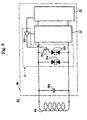
- the invention concerning Claim 1 is an improvement of a tag equipped with a RFID device 16 which is appended to an article 17 and connected to an antenna coil 14 and the antenna coil 14, as shown in Figs. 1 and 2.
- the novel composition is constituted so that it has two or more resonance capacitors 19a-19n mutually connected in parallel and connected in parallel with the antenna coil 14,
- tags 11-13 are independent, even if it has the same resonance frequency, when the tags 11-13 are overlapped, it comes to have a resonance frequency which respectively changes with a mutual inductance between the antenna coils 14 of the tags 11-13.
- each tag 11-13 can not resonate.
- the control circuit 25 suspends the on-off controls, when a resonance frequency of the resonance circuit comprising the antenna coil 14 and the resonance capacitors 19a-19n with the closed switches 24a-24n becomes almost the same as that of a resonance frequency of the un-overlapped single tag 11.
- the tag 11 Since the tag 11 resonates by this procedure, the tag 11 is activated and the tag 11 can be identified.
- the invention concerning Claim 2 as shown in Fig. 7 is characterized by being constituted so that
- a control circuit 25 of the tag 51 operates with the voltage and when the control circuit 25 closes alternatively two or more switches 58a-58b, an inductance of the antenna coil 54 changes.
- the control circuit 25 suspends the on-off controls, when a resonance frequency of the resonance circuit comprising the antenna coil 54 and the resonance capacitor 56a becomes almost the same as that of a resonance frequency of the un-overlapped single tag 51.
- the tag 51 Since the tag 51 resonates by this procedure, the tag 51 is activated and the tag 51 can be identified. It identifies about other tags as well as the above-mentioned procedure.
- the invention concerning Claim 3, as shown in Fig. 8, is characterized by being constituted so that
- a control circuit 25 of the tag 71 operates with the voltage and when the control circuit 25 carries out the on-off controls of two or more switches 78a-78n, total capacitance of the capacitors 77a-77n for capacitance adjustment can be changed.
- the control circuit 25 suspends the on-off controls, when a resonance frequency of the resonance circuit comprising the antenna coil 74 and the capacitors 77a-77n for capacitance adjustment of the closed switches 78a-78n and the resonance capacitor 76a becomes almost the same as that of a resonance frequency of the un-overlapped single tag 71.
- the tag 71 Since the tag 71 resonates by this procedure, the tag 71 is activated and the tag 71 can be identified. It identifies about other tags as well as the above-mentioned procedure. Thus, all the overlapped tags 71 are identified one by one for a short time.
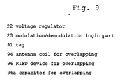
- the invention concerning Claim 4 is an improvement of a tag equipped with a RFID device 96 for overlapping, in which the tag is appended to an article, and a capacitor 96a for overlapping connected to an antenna coil 94 for overlapping and the antenna coil for overlapping 94 are built, as shown in Fig. 9.
- the characteristic composition is that when predetermined number of sheets of tags 91 are overlapped, one of, or both of an inductance of the antenna coil 94 for overlapping and the capacitance of the capacitor 96a for overlapping is/are set up so that a resonance frequency of each overlapped tag 91 is the same as that of a resonance frequency of the un-overlapped single tag 91.
- each tag 91 may resonate when predetermined number of sheets of the tags 91 are beforehand overlapped, if an interrogator oscillates a radio wave of a predetermined frequency to the tags 91 which is beforehand, overlapped with predetermined number of sheets, each tag 91 can respectively resonate.
- the interrogator can identify each tag 91 one by one certainly by communicating with each activated tag 91 which resonates.
- the invention concerning Claim 5 is an invention related to Claim 4, and is furthermore characterized by that besides an antenna coil for overlapping, and a RFID device for overlapping, an antenna coil for un-overlapping and a RFID device for un-overlapping which resonate when not overlapped, are prepared.
- a resonance circuit for independent comprising a capacitor for independence built in the antenna coil for independence and the RFID device for independence, resonates and the tag is identified.
- the resonance circuit for overlapping comprising the antenna coil for overlapping and a capacitor for overlapping, resonates and the tags are identified.
- tags 11-13 have a RFID device 16 connected to an antenna coil 14 and the antenna coil 14.
- the number of tags 11-13 is three, and they are appended to an article 17 respectively, and the article 17 are overlapped with each other.
- Each tag 11-13 is constituted identically.
- the antenna coil 14 is formed in the shape of a swirl of an abbreviation square, as shown in Figs. 3 and 4,
- the RFID device 16 is appended on the base board 18 (Fig. 4), and has two or more resonance capacitors 19a-19n, an ASK modulation circuits 21, a voltage regulator 22, and an modulation/demodulation logic part 23 (Fig. 1).
- Two or more resonance capacitors 19a-19n of each other are connected in parallel and in parallel with the antenna coil 14.
- switches 24a-24n which respectively connect or intercept the capacitors electrically to the antenna coil 14 and the RFID device 16 are connected to two or more resonance capacitors 19a-19n, and on-off controls of the switches is carried out by a control circuit 25.
- Each switches 24a-24n is constituted so that the first series circuits to the n-th series circuits 26a-26n can be opened/closed with a signal from the control circuit 25, respectively.
- a resonance frequency of the resonance circuit comprising the resonance capacitors 19a-19n whose switches 24a-24n are all closed and the antenna coil 14, becomes not more than a resonance frequency of the un-overlapped single tag 11-13 (0.5 to 1 times of a resonance frequency of the un-overlapped tag).
- each above-mentioned resonance capacitor 19a-19n is preferable to be set up respectively according to the amount of shifts of a resonance frequency by overlapping tags 11-13, it may be set up identically.
- the RFID device 16 does not have a battery.
- a memory (not shown) which memorizes data peculiar to an article is prepared in the modulation/demodulation logic part 23.
- the memory is a ROM (read only memory), a RAM (random-access memory), or a nonvolatile memory and so on, and is constituted so that under a control of the modulation/demodulation logic part 23, while data memorized is read according to a read command by data communications of a radio wave from the interrogator 27, a writing of data is performed according to a write command from the interrogator 27.
- an ASK modulation circuit 21 is a circuit which modulates an amplitude of voltage and comprising;
- the modulation switch 21c turns on, the voltage supplied to the antenna coil 14 is restricted to predetermined value (for example, 3V), and if the modulation switch 21c turns off, the voltage supplied to the antenna coil 14 is restricted to predetermined value (for example, 9V).
- a PSK modulation circuit frequency modulation
- a FSK modulation circuit phase modulation
- data such as the amount of money of the cash enclosed with the envelope, a post office and a carrier name which relayed conveyance of the envelope, or the date and time on which the envelope arrived or left for, is memorized.
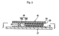
- a mark 31 of Fig. 3 is the first adhesives layer for sticking the base board 18 on the surface of an article 17
- a mark 33 is a cover layer which covers the antenna coil 14 on the base board 18 and the RFID device 16
- a mark 32 is the second adhesives layer for sticking the cover layer 33 on the base board 18.
- the interrogator 27 which identifies tags 11-13 is a RFID controller and have a transceiver antenna 27a, a power supply circuit 27b, a Radio Frequency (RF) circuit 27c and an modulation/demodulation circuit 27d.
- RF Radio Frequency
- a memory 27f, a display 27g, and a 27h of input means are connected to a CPU 27e of the interrogator 27.
- one or two or more sheets of tags may be overlapped on one or two or more sheets of metal plates.
- the metal plate is aluminum foil stuck on the article or coins enclosed with the envelope.
- the RFID device which does not have a battery is exemplified in the embodiment form, the RFID device which has a solar battery or others is also available.
- the articles 17 are three envelopes of registered mails in which bill is enclosed, and tags 11-13 are appended on the articles 17, respectively.
- the data (the amount of money of the cash enclosed with the envelope, a post office and a carrier name which relayed conveyance of the envelope, or the time and date on which the envelope arrived or left off) peculiar to the articles is memorized by the memories of the RFID devices 16 of tags 11-13.
- the distance between the two antenna coils is set to be less than 1mm, a mutual inductance M of two antenna coils in this case is 5.1mH.
- the copper loss r does not affect the resonance frequencies f1 and f2.
- the interrogator 27 communicates with the tag 11 first.
- the minimum voltage V0 between A-B which can activate a tag 11 is memorized, that is, the minimum voltage V0 between A-B when the tag 11 resonates is memorized.
- the control circuit 25 compares the signal (actual voltage VAB between A-B) and the voltage V0 from the modulation/demodulation logic part 23, and if it becomes VAB ⁇ V0, it opens the switch 24a toward the switch 24n in order, and the total capacitance of resonance capacitors 19a-19n is decreased.
- control circuit 25 suspends the on-off controls of the switches 24a-24n.
- the tag 11 resonates on a radio wave which the interrogator 27 oscillates.
- the radio wave (a polling signal) oscillated from the interrogator 27 is a digital signal formed into 2 value.
- the digital signal is emitted from a signal generator (not shown) of the interrogator 27, superimposed on the carrier of a predetermined frequency by a modulation/demodulation circuits 27d, namely, the digital signal is modulated.
- the modulated signal is amplified and oscillated from the transceiver antenna 27a.
- the ASK amplitude modulation
- the FSK frequency modulation
- the PSK phase modulation
- the interrogator 27 reads the peculiar information memorized by the memory of the RFID device 16 of the resonating tag 11.
- the voltage produced by the electromagnetic induction is impressed to the capacitor 19
- the voltage regulator 22 rectifies and stabilizes this voltage, and supplies to the modulation/demodulation logic part 23.
- the RFID device 16 activates the RFID device 16, only a signal required for a demodulation is derived by the modulation/demodulation logic part 23, the polling signal of the original digital signal is made to reproduce, and the data of the envelopes 17 including the enclosed amount of money peculiar to an envelope 17 derived from the memory, is oscillated to the interrogator.
- An oscillation of this data formed into 2 value, for example, the enclosure amount of money is performed by amplifying and modulating with the ASK modulation 21 of the RFID device 16, and oscillating from the antenna coil 14.
- the peculiar information on the concerned envelope 17 can be checked by the display 27g.
- the data to be written (for example, time and a post office name in which the check is performed, i.e., the time and the post office in which contents about the envelope in the tag is read, etc.), are inputted by input means 27h, and oscillated to the tag 11.
- the data is written in the memory of the RFID device 16.
- the interrogator 27 communicates with the tag 12 by the above-mentioned procedure, if the writing to the memory of the RFID device 16 of the tag 12 is completed, a signal is sent to the control circuit 25 from the modulation/demodulation logic part 23 of the tag 12, all the switches 24a-24n are closed.
- the interrogator 27 communicates the remaining tag 13 by the above-mentioned procedure, if the writing to the memory of the RFID device 16 of a tag 13 is completed, a signal is sent to the control circuit 25 from the modulation/demodulation logic part 23 of the tag 13, and all the switches 24a-24n are closed.
- a metal plate such as a coin also can be enclosed with the envelope 17.
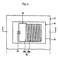
- Figs. 5 and 6 show the second embodiment form of the present invention.
- the present embodiment form it has a magnetic material 44a from which the antenna coil 44 serves as magnetic core, main part of coil 44b wound around the magnetic material 44a.
- a plate, a cylinder, a solid prism, a hollow cylinder, etc. may be used.
- the hollow cylinder may be one in which the cylinder is formed by an assembling a plurality of arc-shaped pieces, or one in which the cylinder is formed by a thin film or foil.
- the soft magnetic metal thin film of the above-mentioned (1) it is preferable to use a film with a thickness of 5-250 micrometers made of an iron base amorphous, a cobalt base amorphous, a permalloy or a silicon steel, as the insulating thin film and preferable to use an insulating resin film with a thickness of 5-50 micrometers made of a polyester film, a poly vinylidene chloride, a poly vinyl chloride, a polyethylene terephthalates (PET).
- PET polyethylene terephthalates
- an insulated paper is sufficient as the insulating thin film.
- the powder of the soft magnetic metal of above-mentioned (2) or (3) it is preferable to use a carbonyl iron powder or a reduced iron powder with a diameter of 0.1-30 micrometers.
- the flake of the soft magnetic metal made of the iron, the permalloy and the amorphous alloy, etc. are divided by the atomize method, and are obtained by mechanically fabricating the soft magnetic metal powder to be flat with a thickness of 0.1-10 micrometers.
- the constituted and overlaped tag 41 has the feature that a mutual inductance with other tag 41 or a metal plate is small, when overlaped on other tags 41 or the metal plate.
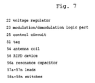
- Fig. 7 shows the third embodiment form of the present invention.
- n leads 57a-57n whose ends are connected with predetermined intervals to the winding of an antenna coil 54, are connected to a RFID device 56, n switches 58a-58n are respectively prepared in the leads 57a-57n, the control circuit 25 closes n pieces of the switches 58a-58ns alternatively.
- n leads 57a-57n are connected to the antenna coil 54 for every 1/n of the antenna coil.
- each switches 58a-58n prepared in leads 57a-57n and connects or intercepts electrically the antenna coil 54 and the RFID device 56, respectively.
- a resonance frequency of the resonance circuit comprising the antenna coil 54 and the resonance capacitor 56a becomes not more than a resonance frequency of the un-overlapped single tag 51 (0.5-1 times to a resonance frequency of the un-overlapped tag).
- n leads 57a-57n are connected for every 1/n of the total number of turns of the antenna coil 54, it may be connected changing respectively, according to the amount of shifts of a resonance frequency by overlapping of the tag 51
- each tag 51 before the control circuit 25 operates, since only the switch 58a closes, if the tags 51 are overlapped and a radio wave of a predetermined frequency is oscillated from the interrogator, as same in the first embodiment form, a mutual inductance arises among the antenna coils 54 of each tag 51, and a resonance frequency of each tag 51 changes.
- the interrogator communicates with one tag 51 in two or more tags 51.
- the minimum voltage V0 between A-B to activate the tag 51 that is, the minimum voltage V0 between A-B when the tag 51 resonates is memorized.
- the control circuit 25 compares a signal from the modulation/demodulation logic part 23 (actual voltage VAB between A-B) and the voltage V0, and if it becomes VAB ⁇ V0, it opens the switch 58a and change the state into the state where only the switch 58b is closed, and reduces the number of turns to which the current of the antenna coil 54 flows.
- control circuit 25 suspends on-off controls of the switches 58a-58n.
- a tag 51 resonates with a radio wave which is oscillated by the interrogator.
- the interrogator writes a predetermined matter in the memory, after reading the peculiar information memorized in the memory of the RFID device 56 in the resonated tag 51.
- the interrogator communicates with another tag by the above-mentioned procedure, if the writing to the memory of the RFID device of the tag is completed, a signal is sent to the control circuit from the modulation/demodulation logic part of the tag and it returns to the first state.
- a metal plate such as coin may be enclosed with an envelope which is an article.
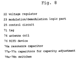
- Fig. 8 shows the forth embodiment of the present invention.
- the present embodiment form it is constituted so that two or more capacitors 77a-77n for capacitance adjustment are connected to an antenna coil 74 in series and connected each other in parallel, two or more switches 78a-78n are respectively connected to the capacitors 77a-77n for capacitance adjustment, furthermore, the control circuit 25 may carry out on-off controls of the switches 78a-78n.
- switches 78a-78n are connected or intercepted electrically two or more capacitors 77a-77n for capacitance adjustment to the antenna coil 74 and the RFID device 76, respectively.
- Each switch 78a-78n is constituted so that the first series circuits to the n-Th series circuits 79a-79n may be opened and closed with a signal from the control circuit 25, respectively.
- a resonance capacitor 76a is prepared in the RFID device 76.
- the control circuit 25 carries out the on-off control of each above-mentioned switch 78a-78n, the total capacitance of the capacitors 77a-77n for capacitance adjustment changes, and the resonance frequency of a resonance circuit comprising the antenna coil 74, the capacitors 77a-77n for capacitance adjustment with the closed switches 78a-78n and the resonance capacitor 76a can be changed to be the resonance frequency of an un-overlaped single tag 71.
- a resonance frequency of the resonance circuit comprising the antenna coil 74, the capacitors 77a-77n for capacitance adjustment with the closed switches 78a-78n and the resonance capacitor 76a may become not more than a resonance frequency of the un-overlaped single tag 71 (0.5-1 times of a resonance frequency of the un-overlapped tag).
- the switches 78a-78n are set to the state where all are closed.
- the total capacitance of the capacitors 77a-77n for capacitance adjustment is set up more greatly than the capacitance of the resonance capacitor 76a.
- the capacitance of the resonance capacitor 76a is set to 210pF
- the capacitors 77a-77n for capacitance adjustment and the resonance capacitor 76a are set to about 206pF, the capacitors 77a-77n for capacitance adjustment can be neglected.
- each capacitors 77a-77n for capacitance adjustment that the capacitance is changed respectively, and the capacitance is set up to according to the amount of shifts of a resonance frequency by overlapping of the tags 71, but the capacitance is also set up identically.
- the capacitors 77a-77n for capacitance adjustment and the control circuit 25 are equipped out side of the RFID device 76, the capacitors for capacity adjustment and the control circuit can be also equipped inside of the RFID device.
- the interrogator communicates with one tag 71 among two or more tags 71.
- the minimum voltage V0 between A-B by which the tag 71 is activated that is, the minimum voltage V0 between A-B when the tag 71 resonates, is memorized.
- the control circuit 25 compares the signal (actual voltage VAB between A-B) and the voltage V0 from the modulation/demodulation logic part 23, if it becomes to VAB ⁇ V0, and decreases the total capacitance of the capacitors 77a-77n for capacitance adjustment by opening the switch sequentially from the switch 78a to the switch 78n in order.
- control circuit 25 suspends the on-off controls of the switches 78a-78n.
- the tag 71 resonates with a radio wave which the interrogator oscillates.
- the interrogator after reading the peculiar information memorized in the memory of the RFID element 76 of the resonating tag 71, writes a predetermined matter in the memory.
- a signal is sent to the control circuit 25 from the modulation/demodulation logic part 23 of the tag 71 and it is set up to be the first state by closing the switches 78a-78n altogether.
- the interrogator communicates with another tag by the above-mentioned procedure, if the writing to the memory of the RFID element of the tag is completed, a signal is sent to the control circuit from modulation/demodulation logic part of the tag and it is set up to be the first state.
- all the switches of the tags whose communications are completed may be change into the state where they are opened.
- a metal plate such as a coin may be enclosed with an envelope which is an article.
- Fig. 9 shows the fifth embodiment form of the present invention.
- a tag 91 is equipped with an antenna coil 94 for overlapping and a RFID element 96 for overlapping which the antenna coil 94 for overlapping is connected to and a capacitor 96a for overlapping is built in.
- either or both of the inductance of the antenna coil 94 for overlapping and the capacitance of capacitor 96a for overlapping is/are set up so that a resonance frequency of each of the tags 91 is identically to be a resonance frequency of the un-overlapped single tag 91.
- each tag 91 when only predetermined number of sheets of tag 91 are overlapped beforehand, since an inductance of the antenna coil 94 for overlapping and a capacitance of capacitor 96a for overlapping are adjusted so that each tag 91 resonates, if the interrogator oscillates a radio wave of predetermined frequency to the tag 91 overlapped only predetermined number of sheets, each tag 91 resonates, respectively.
- the interrogator can identifies each tag 91 certainly by communicating one by one with each above-mentioned tag 91 resonating and activating.
- an antenna coil for independence and a RFID device for independence which resonate when the tag is not overlapped, can be equipped with the tag.
- the resonance circuit for overlapping comprising the antenna coil for overlapping and the capacitor for overlapping, the tag is oscillated and identified.
- the tag of the second embodiment form namely, the tag is comprised with a magnetic material and a main part of a coil, can be used.
- a resonance frequency of a resonance circuit comprising an antenna coil and two or more resonance capacitors can be changed, by connecting the resonance capacitors in parallel with the antenna coil and in parallel with each other, connecting two or more switches to the resonance capacitors, respectively, furthermore, operating on-off controls of the switches by a control circuit, even if resonance frequency of each tag changes by overlapping two or more tags, or a tag and a metal plate, by changing total capacitance of the resonance capacitors, resonance frequency of the resonance circuit comprising the antenna coil and the resonance capacitor with the closed switch of each tag can be set up to be almost the same with that of the resonance frequency of the un-overlapped tag.
- each tag is identified one by one for a short time.
- resonance frequency of the resonance circuit comprising an antenna coil and a resonance capacitor in the RFID device, can be changed, by connecting ends of two or more leads to a winding of the antenna coil with predetermined intervals and the other ends to a RFID device, having two or more switches in the leads, furthermore, closing arbitrary switches alternatively by a control circuit, even if a resonance frequency of each tag changes by overlapping two or more tags, or a tag and a metal plate, a resonance frequency of the resonance circuit comprising the antenna coil and the resonance capacitor of each tag can be set up to be almost the same with that of the resonance frequency of the un-overlapped single tag by changing the inductance of the antenna coil.
- each tag is identified one by one for a short time.
- a resonance frequency of a resonance circuit comprising an antenna coil, a capacitor for capacity adjustment and a resonance capacitor can be changed, by connecting two or more capacitors for capacity adjustment to the antenna coil in series and each other in parallel, connecting two or more switches to the capacitors for capacity adjustment, respectively, furthermore, operating on-off controls of the switches by a control circuit, even if resonance frequency of each tag changes by overlapping two or more tags, or tag and metal plate, a resonance frequency of the resonance circuit comprising the antenna coil, the capacitor for capacity adjustment with the closed switch and the resonance capacitor can be set up to be almost the same with that of the resonance frequency of the un-overlapped single tag by changing total capacitance of the capacitor for capacity adjustment.
- each tag is identified one by one for a short time.
- each tag when predetermined number of tags are overlapped, if one of or both of a capacitance of the inductance of an antenna coil for overlapping and the capacitor for overlapping is/are set up so that a resonance frequency of each overlapped tag becomes the same with that of resonance frequency of the un-overlapped single tag, when an interrogator oscillates a radio wave of a predetermined frequency to the tags overlapped only predetermined number of sheets, each tag resonate, respectively.
- an antenna coil for independence and a RFID device for independence which resonate when tag is not overlapped, are equipped with an antenna coil for overlapping and a RFID device for overlapping, when a tag is independent, a tag is identified by resonating resonance circuit for independence comprising the antenna coil for independence and the capacitor for independent built in the RFID device for independence.
- tags are overlapped, the tags are identified by resonating a resonance circuit for overlapping constituted by an antenna coil for overlapping and a capacitor for overlapping.
- the tags can be identified regardless of whether the tags are overlapped or not.
Landscapes
- Engineering & Computer Science (AREA)
- Computer Hardware Design (AREA)
- Microelectronics & Electronic Packaging (AREA)
- Physics & Mathematics (AREA)
- General Physics & Mathematics (AREA)
- Theoretical Computer Science (AREA)
- Computer Networks & Wireless Communication (AREA)
- Artificial Intelligence (AREA)
- Computer Vision & Pattern Recognition (AREA)
- Near-Field Transmission Systems (AREA)
- Burglar Alarm Systems (AREA)
Applications Claiming Priority (3)
| Application Number | Priority Date | Filing Date | Title |
|---|---|---|---|
| JP10320153A JP2000151480A (ja) | 1998-11-11 | 1998-11-11 | 重畳タグの識別方式 |
| JP32015398 | 1998-11-11 | ||
| PCT/JP1999/006161 WO2000028674A1 (fr) | 1998-11-11 | 1999-11-05 | Procede permettant d'identifier des etiquettes chevauchantes |
Publications (2)
| Publication Number | Publication Date |
|---|---|
| EP1061663A1 true EP1061663A1 (fr) | 2000-12-20 |
| EP1061663A4 EP1061663A4 (fr) | 2004-06-30 |
Family
ID=18118306
Family Applications (1)
| Application Number | Title | Priority Date | Filing Date |
|---|---|---|---|
| EP99954393A Withdrawn EP1061663A4 (fr) | 1998-11-11 | 1999-11-05 | Procede permettant d'identifier des etiquettes chevauchantes |
Country Status (3)
| Country | Link |
|---|---|
| EP (1) | EP1061663A4 (fr) |
| JP (1) | JP2000151480A (fr) |
| WO (1) | WO2000028674A1 (fr) |
Cited By (16)
| Publication number | Priority date | Publication date | Assignee | Title |
|---|---|---|---|---|
| WO2002050758A1 (fr) * | 2000-12-20 | 2002-06-27 | Fraunhofer-Gesellschaft zur Förderung der angewandten Forschung e. V. | Dispositif et procede de lecture simultanee de transducteurs inductifs passifs |
| DE10158442A1 (de) * | 2001-12-01 | 2003-06-26 | Atmel Germany Gmbh | Sende- und Empfangseinrichtung für eine kontaktlose Datenübertragung |
| EP1387313A3 (fr) * | 2002-07-30 | 2004-06-23 | Omron Corporation | Etiquette d'identification radio fréquence avec des moyens d'ajustement de sa fréquence de résonance et procédé anticollision |
| US6870461B2 (en) | 2001-12-01 | 2005-03-22 | Atmel Germany Gmbh | Integrated receiving/backscattering arrangement for contactless data transmission |
| EP1327958A4 (fr) * | 2000-08-15 | 2005-05-11 | Omron Tateisi Electronics Co | Support de communication sans contact et systeme de communication sans contact |
| WO2005093455A1 (fr) * | 2004-03-29 | 2005-10-06 | Magellan Technology Pty Ltd. | Chaine d'approvisionnement et/ou authentification d'un article, systeme, procede et dispositif de tracage, d'identification et de surveillance |
| WO2005104022A1 (fr) * | 2004-04-08 | 2005-11-03 | 3M Innovative Properties Company | Etiquettes d'identification par radio-frequence (rfid) a frequence variable |
| WO2005121832A1 (fr) * | 2004-06-09 | 2005-12-22 | Magellan Technology Pty Ltd | Procede, systeme et appareil de gestion de documents |
| FR2878386A1 (fr) * | 2004-11-23 | 2006-05-26 | St Microelectronics Sa | Procede d'anticollision pour transpondeurs electromagnetiques |
| FR2899360A1 (fr) * | 2006-02-01 | 2007-10-05 | Spacecode Sa | Produit conducteur comportant une etiquette electronique, procede et dispositif d'identification de tels produits |
| EP1865445A2 (fr) | 2006-06-08 | 2007-12-12 | Sony Ericsson Mobile Communications Japan, Inc. | Appareil de terminal de communications sans fil et son procédé de contrôle |
| US7315248B2 (en) | 2005-05-13 | 2008-01-01 | 3M Innovative Properties Company | Radio frequency identification tags for use on metal or other conductive objects |
| WO2009115115A1 (fr) * | 2008-03-18 | 2009-09-24 | Nokia Corporation | Commande de la tension de sortie d'une antenne dans un dispositif de communication en champ proche |
| EP1267303B1 (fr) * | 2001-06-11 | 2011-07-27 | HID Global GmbH | Transpondeur |
| EP2393044A1 (fr) * | 2005-07-22 | 2011-12-07 | Winstead Assets Ltd. | produit conducteur comportant une étiquette électronique |
| WO2021133651A1 (fr) * | 2019-12-28 | 2021-07-01 | Avery Dennison Retail Information Services, Llc | Ensembles d'accord pour puces rfid |
Families Citing this family (10)
| Publication number | Priority date | Publication date | Assignee | Title |
|---|---|---|---|---|
| JP3896965B2 (ja) | 2002-01-17 | 2007-03-22 | 三菱マテリアル株式会社 | リーダ/ライタ用アンテナ及び該アンテナを備えたリーダ/ライタ |
| WO2006075800A1 (fr) * | 2005-01-17 | 2006-07-20 | Canon Kabushiki Kaisha | Etiquette a resonance, procede pour modifier de maniere reversible les caracteristiques de resonance d'un circuit de resonance et element capacitif |
| US7367496B2 (en) | 2005-06-06 | 2008-05-06 | International Business Machines Corporation | Detecting wear through use of information-transmitting devices |
| US7639095B2 (en) * | 2005-09-28 | 2009-12-29 | Tyco Electronics Belgium Ec N.V. | Circuit and method for contact-less transmission |
| CN101501991B (zh) * | 2006-06-27 | 2012-06-13 | 传感电子公司 | 带有动态阻抗匹配的谐振电路调谐系统 |
| KR100941110B1 (ko) * | 2008-02-01 | 2010-02-10 | 한국과학기술원 | 인덕티브 커플링 통신에서의 인덕턴스 보상 방법 및 장치 |
| EP2423855B1 (fr) * | 2010-08-24 | 2012-10-03 | Siemens Aktiengesellschaft | Transpondeur RFID couplé inductif |
| JP7376463B2 (ja) * | 2020-02-04 | 2023-11-08 | 富士フイルム株式会社 | 非接触式通信媒体、磁気テープカートリッジ、及び非接触式通信媒体の製造方法 |
| US11809926B2 (en) | 2020-02-04 | 2023-11-07 | Fujifilm Corporation | Noncontact communication medium, magnetic tape cartridge, and manufacturing method of noncontact communication medium |
| JPWO2024162274A1 (fr) | 2023-02-01 | 2024-08-08 |
Family Cites Families (6)
| Publication number | Priority date | Publication date | Assignee | Title |
|---|---|---|---|---|
| US5541604A (en) * | 1993-09-03 | 1996-07-30 | Texas Instruments Deutschland Gmbh | Transponders, Interrogators, systems and methods for elimination of interrogator synchronization requirement |
| JPH0884094A (ja) * | 1994-09-05 | 1996-03-26 | Texas Instr Deutschland Gmbh | 呼掛部の同期要求を不要にするトランスポンダ、呼掛部のシステムと方法 |
| DE4438286C2 (de) * | 1994-10-26 | 2002-09-12 | Siemens Ag | System zur kontaktlosen Energie- und Datenübertragung |
| JPH10187916A (ja) * | 1996-12-27 | 1998-07-21 | Rohm Co Ltd | 非接触icカード通信システムにおける応答器 |
| FR2757952B1 (fr) * | 1996-12-27 | 1999-03-19 | Gemplus Card Int | Transpondeur radioelectrique muni d'une antenne et d'un circuit de desaccord en frequence |
| GB2321726A (en) * | 1997-01-30 | 1998-08-05 | Motorola Inc | Apparatus and method for regulating power on a contactless portable data carrier |
-
1998
- 1998-11-11 JP JP10320153A patent/JP2000151480A/ja active Pending
-
1999
- 1999-11-05 WO PCT/JP1999/006161 patent/WO2000028674A1/fr not_active Ceased
- 1999-11-05 EP EP99954393A patent/EP1061663A4/fr not_active Withdrawn
Cited By (27)
| Publication number | Priority date | Publication date | Assignee | Title |
|---|---|---|---|---|
| EP1327958A4 (fr) * | 2000-08-15 | 2005-05-11 | Omron Tateisi Electronics Co | Support de communication sans contact et systeme de communication sans contact |
| US6952167B2 (en) | 2000-08-15 | 2005-10-04 | Omron Corporation | Noncontact communication medium and noncontact communication system |
| US6824054B2 (en) | 2000-12-20 | 2004-11-30 | Fraunhofer-Gesellschaft Zur Foerderung Der Angewandten Forshcung E.V. | Apparatus and method for simultaneously reading out of passive inductive transponders |
| EP1357503A1 (fr) * | 2000-12-20 | 2003-10-29 | Fraunhofer-Gesellschaft Zur Förderung Der Angewandten Forschung E.V. | Transpondeur à circuit résonnant accordé |
| WO2002050758A1 (fr) * | 2000-12-20 | 2002-06-27 | Fraunhofer-Gesellschaft zur Förderung der angewandten Forschung e. V. | Dispositif et procede de lecture simultanee de transducteurs inductifs passifs |
| EP1267303B1 (fr) * | 2001-06-11 | 2011-07-27 | HID Global GmbH | Transpondeur |
| DE10256099A1 (de) * | 2001-12-01 | 2004-06-17 | Atmel Germany Gmbh | Sende- und Empfangseinrichtung für eine kontaktlose Datenübertragung |
| DE10158442B4 (de) * | 2001-12-01 | 2004-11-25 | Atmel Germany Gmbh | Sende- und Empfangseinrichtung für eine kontaktlose Datenübertragung |
| US6870461B2 (en) | 2001-12-01 | 2005-03-22 | Atmel Germany Gmbh | Integrated receiving/backscattering arrangement for contactless data transmission |
| DE10158442A1 (de) * | 2001-12-01 | 2003-06-26 | Atmel Germany Gmbh | Sende- und Empfangseinrichtung für eine kontaktlose Datenübertragung |
| EP1387313A3 (fr) * | 2002-07-30 | 2004-06-23 | Omron Corporation | Etiquette d'identification radio fréquence avec des moyens d'ajustement de sa fréquence de résonance et procédé anticollision |
| WO2005093455A1 (fr) * | 2004-03-29 | 2005-10-06 | Magellan Technology Pty Ltd. | Chaine d'approvisionnement et/ou authentification d'un article, systeme, procede et dispositif de tracage, d'identification et de surveillance |
| US7304577B2 (en) | 2004-04-08 | 2007-12-04 | 3M Innovative Properties Company | Variable frequency radio frequency identification (RFID) tags |
| WO2005104022A1 (fr) * | 2004-04-08 | 2005-11-03 | 3M Innovative Properties Company | Etiquettes d'identification par radio-frequence (rfid) a frequence variable |
| US7132946B2 (en) | 2004-04-08 | 2006-11-07 | 3M Innovative Properties Company | Variable frequency radio frequency identification (RFID) tags |
| WO2005121832A1 (fr) * | 2004-06-09 | 2005-12-22 | Magellan Technology Pty Ltd | Procede, systeme et appareil de gestion de documents |
| FR2878386A1 (fr) * | 2004-11-23 | 2006-05-26 | St Microelectronics Sa | Procede d'anticollision pour transpondeurs electromagnetiques |
| US7315248B2 (en) | 2005-05-13 | 2008-01-01 | 3M Innovative Properties Company | Radio frequency identification tags for use on metal or other conductive objects |
| EP2393044A1 (fr) * | 2005-07-22 | 2011-12-07 | Winstead Assets Ltd. | produit conducteur comportant une étiquette électronique |
| FR2899360A1 (fr) * | 2006-02-01 | 2007-10-05 | Spacecode Sa | Produit conducteur comportant une etiquette electronique, procede et dispositif d'identification de tels produits |
| EP1865445A2 (fr) | 2006-06-08 | 2007-12-12 | Sony Ericsson Mobile Communications Japan, Inc. | Appareil de terminal de communications sans fil et son procédé de contrôle |
| EP1865445A3 (fr) * | 2006-06-08 | 2008-09-10 | Sony Ericsson Mobile Communications Japan, Inc. | Appareil de terminal de communications sans fil et son procédé de contrôle |
| US8406686B2 (en) | 2006-06-08 | 2013-03-26 | Sony Mobile Communications Japan, Inc. | Wireless communication terminal apparatus and method of controlling same |
| WO2009115115A1 (fr) * | 2008-03-18 | 2009-09-24 | Nokia Corporation | Commande de la tension de sortie d'une antenne dans un dispositif de communication en champ proche |
| WO2021133651A1 (fr) * | 2019-12-28 | 2021-07-01 | Avery Dennison Retail Information Services, Llc | Ensembles d'accord pour puces rfid |
| CN115066685A (zh) * | 2019-12-28 | 2022-09-16 | 艾利丹尼森零售信息服务有限公司 | 用于射频识别芯片的调谐组件 |
| US12056553B2 (en) | 2019-12-28 | 2024-08-06 | Avery Dennison Retail Information Services Llc | Tuning assemblies for RFID chips |
Also Published As
| Publication number | Publication date |
|---|---|
| JP2000151480A (ja) | 2000-05-30 |
| WO2000028674A1 (fr) | 2000-05-18 |
| EP1061663A4 (fr) | 2004-06-30 |
Similar Documents
| Publication | Publication Date | Title |
|---|---|---|
| US6840440B2 (en) | Identifying system of overlapped tag | |
| EP1061663A1 (fr) | Procede permettant d'identifier des etiquettes chevauchantes | |
| US6346884B1 (en) | Apparatus for identifying an article | |
| US8113439B2 (en) | Antenna apparatus | |
| US6927738B2 (en) | Apparatus and method for a communication device | |
| CA2284600C (fr) | Appareil de decouplage magnetique d'etiquette a identification par radiofrequence | |
| JP4168597B2 (ja) | トランスポンダ用アンテナ | |
| US7508305B2 (en) | Packing material, tag, certificate, paper money, and securities | |
| US8256684B2 (en) | Antenna apparatus | |
| JP2007524942A (ja) | 電磁波により与えられる受動送信機受信機装置 | |
| KR20010090811A (ko) | 태그를 그 주위로부터 자기적으로 감결합하기 위한 병렬공진 회로를 구비한 무선 식별 태그 | |
| JP5026522B2 (ja) | 受動共振回路を用いた高周波通信用トランスポンダの最適化された読取り方法およびシステム | |
| JP3476000B2 (ja) | 重畳したタグの識別方式 | |
| JP3607217B2 (ja) | データキャリア構造及びその製造方法 | |
| JP4578728B2 (ja) | 携帯型機器 | |
| WO2002099764A1 (fr) | Systeme de communication de donnees a alimentation capacitive comprenant un dispositif d'etiquette et de support de circuit | |
| JP3399505B2 (ja) | 金属ケース内の物品の識別装置 | |
| JPH10162262A (ja) | 無線タグおよびその製造方法 |
Legal Events
| Date | Code | Title | Description |
|---|---|---|---|
| PUAI | Public reference made under article 153(3) epc to a published international application that has entered the european phase |
Free format text: ORIGINAL CODE: 0009012 |
|
| AK | Designated contracting states |
Kind code of ref document: A1 Designated state(s): AT BE CH CY DE DK ES FI FR GB GR IE IT LI LU MC NL PT SE |
|
| 17P | Request for examination filed |
Effective date: 20001114 |
|
| RBV | Designated contracting states (corrected) |
Designated state(s): DE FR GB |
|
| A4 | Supplementary search report drawn up and despatched |
Effective date: 20040519 |
|
| RIC1 | Information provided on ipc code assigned before grant |
Ipc: 7G 06K 19/07 A |
|
| 17Q | First examination report despatched |
Effective date: 20040820 |
|
| STAA | Information on the status of an ep patent application or granted ep patent |
Free format text: STATUS: THE APPLICATION IS DEEMED TO BE WITHDRAWN |
|
| 18D | Application deemed to be withdrawn |
Effective date: 20080703 |