EP1061546A2 - Spacers used for picture display devices and a method of producing the same - Google Patents
Spacers used for picture display devices and a method of producing the same Download PDFInfo
- Publication number
- EP1061546A2 EP1061546A2 EP00112779A EP00112779A EP1061546A2 EP 1061546 A2 EP1061546 A2 EP 1061546A2 EP 00112779 A EP00112779 A EP 00112779A EP 00112779 A EP00112779 A EP 00112779A EP 1061546 A2 EP1061546 A2 EP 1061546A2
- Authority
- EP
- European Patent Office
- Prior art keywords
- spacers
- plate
- spacer
- glass
- face plate
- Prior art date
- Legal status (The legal status is an assumption and is not a legal conclusion. Google has not performed a legal analysis and makes no representation as to the accuracy of the status listed.)
- Granted
Links
- 125000006850 spacer group Chemical group 0.000 title claims abstract description 280
- 238000000034 method Methods 0.000 title claims description 59
- 239000011521 glass Substances 0.000 claims abstract description 99
- 229910052751 metal Inorganic materials 0.000 claims abstract description 88
- 239000002184 metal Substances 0.000 claims abstract description 88
- 238000010304 firing Methods 0.000 claims abstract description 57
- 229910052710 silicon Inorganic materials 0.000 claims abstract description 16
- 229910052782 aluminium Inorganic materials 0.000 claims abstract description 15
- 229910052802 copper Inorganic materials 0.000 claims abstract description 14
- 229910052725 zinc Inorganic materials 0.000 claims abstract description 14
- 229910052718 tin Inorganic materials 0.000 claims abstract description 13
- 229910052749 magnesium Inorganic materials 0.000 claims abstract description 11
- 229920005989 resin Polymers 0.000 claims description 55
- 239000011347 resin Substances 0.000 claims description 55
- OAICVXFJPJFONN-UHFFFAOYSA-N Phosphorus Chemical compound [P] OAICVXFJPJFONN-UHFFFAOYSA-N 0.000 claims description 41
- 238000000465 moulding Methods 0.000 claims description 28
- 239000000843 powder Substances 0.000 claims description 27
- VYPSYNLAJGMNEJ-UHFFFAOYSA-N Silicium dioxide Chemical compound O=[Si]=O VYPSYNLAJGMNEJ-UHFFFAOYSA-N 0.000 claims description 25
- GWEVSGVZZGPLCZ-UHFFFAOYSA-N Titan oxide Chemical group O=[Ti]=O GWEVSGVZZGPLCZ-UHFFFAOYSA-N 0.000 claims description 24
- 239000000919 ceramic Substances 0.000 claims description 24
- 239000000945 filler Substances 0.000 claims description 23
- WMWLMWRWZQELOS-UHFFFAOYSA-N bismuth(iii) oxide Chemical compound O=[Bi]O[Bi]=O WMWLMWRWZQELOS-UHFFFAOYSA-N 0.000 claims description 18
- XOLBLPGZBRYERU-UHFFFAOYSA-N tin dioxide Chemical compound O=[Sn]=O XOLBLPGZBRYERU-UHFFFAOYSA-N 0.000 claims description 16
- 239000000203 mixture Substances 0.000 claims description 13
- 239000000377 silicon dioxide Substances 0.000 claims description 11
- 239000012298 atmosphere Substances 0.000 claims description 9
- QVGXLLKOCUKJST-UHFFFAOYSA-N atomic oxygen Chemical compound [O] QVGXLLKOCUKJST-UHFFFAOYSA-N 0.000 claims description 9
- 239000001301 oxygen Substances 0.000 claims description 9
- 229910052760 oxygen Inorganic materials 0.000 claims description 9
- 239000002245 particle Substances 0.000 claims description 8
- 229910052681 coesite Inorganic materials 0.000 claims description 7
- 229910052906 cristobalite Inorganic materials 0.000 claims description 7
- 238000010438 heat treatment Methods 0.000 claims description 7
- 229910052682 stishovite Inorganic materials 0.000 claims description 7
- 229910052905 tridymite Inorganic materials 0.000 claims description 7
- 239000000126 substance Substances 0.000 claims description 3
- 238000011049 filling Methods 0.000 claims description 2
- 230000003647 oxidation Effects 0.000 abstract description 9
- 238000007254 oxidation reaction Methods 0.000 abstract description 9
- 239000010410 layer Substances 0.000 description 86
- 239000000047 product Substances 0.000 description 29
- KFZMGEQAYNKOFK-UHFFFAOYSA-N Isopropanol Chemical compound CC(C)O KFZMGEQAYNKOFK-UHFFFAOYSA-N 0.000 description 18
- 239000010949 copper Substances 0.000 description 12
- 238000002474 experimental method Methods 0.000 description 12
- MCMNRKCIXSYSNV-UHFFFAOYSA-N Zirconium dioxide Chemical compound O=[Zr]=O MCMNRKCIXSYSNV-UHFFFAOYSA-N 0.000 description 10
- 230000003247 decreasing effect Effects 0.000 description 7
- 230000001965 increasing effect Effects 0.000 description 7
- 239000011159 matrix material Substances 0.000 description 7
- PXHVJJICTQNCMI-UHFFFAOYSA-N Nickel Chemical compound [Ni] PXHVJJICTQNCMI-UHFFFAOYSA-N 0.000 description 6
- 230000007423 decrease Effects 0.000 description 6
- 239000000853 adhesive Substances 0.000 description 5
- 230000001070 adhesive effect Effects 0.000 description 5
- 239000011230 binding agent Substances 0.000 description 5
- 238000010894 electron beam technology Methods 0.000 description 5
- 239000007789 gas Substances 0.000 description 5
- 238000007639 printing Methods 0.000 description 5
- 238000007650 screen-printing Methods 0.000 description 5
- 229910052797 bismuth Inorganic materials 0.000 description 4
- 239000005388 borosilicate glass Substances 0.000 description 4
- DOIRQSBPFJWKBE-UHFFFAOYSA-N dibutyl phthalate Chemical compound CCCCOC(=O)C1=CC=CC=C1C(=O)OCCCC DOIRQSBPFJWKBE-UHFFFAOYSA-N 0.000 description 4
- 238000004455 differential thermal analysis Methods 0.000 description 4
- 239000002270 dispersing agent Substances 0.000 description 4
- BASFCYQUMIYNBI-UHFFFAOYSA-N platinum Chemical compound [Pt] BASFCYQUMIYNBI-UHFFFAOYSA-N 0.000 description 4
- 229920002379 silicone rubber Polymers 0.000 description 4
- 239000004945 silicone rubber Substances 0.000 description 4
- 238000002411 thermogravimetry Methods 0.000 description 4
- 238000009834 vaporization Methods 0.000 description 4
- WVDDGKGOMKODPV-UHFFFAOYSA-N Benzyl alcohol Chemical compound OCC1=CC=CC=C1 WVDDGKGOMKODPV-UHFFFAOYSA-N 0.000 description 3
- KDLHZDBZIXYQEI-UHFFFAOYSA-N Palladium Chemical compound [Pd] KDLHZDBZIXYQEI-UHFFFAOYSA-N 0.000 description 3
- XUIMIQQOPSSXEZ-UHFFFAOYSA-N Silicon Chemical compound [Si] XUIMIQQOPSSXEZ-UHFFFAOYSA-N 0.000 description 3
- XLOMVQKBTHCTTD-UHFFFAOYSA-N Zinc monoxide Chemical compound [Zn]=O XLOMVQKBTHCTTD-UHFFFAOYSA-N 0.000 description 3
- 230000002159 abnormal effect Effects 0.000 description 3
- 229910052910 alkali metal silicate Inorganic materials 0.000 description 3
- PNEYBMLMFCGWSK-UHFFFAOYSA-N aluminium oxide Inorganic materials [O-2].[O-2].[O-2].[Al+3].[Al+3] PNEYBMLMFCGWSK-UHFFFAOYSA-N 0.000 description 3
- 238000010586 diagram Methods 0.000 description 3
- 238000006073 displacement reaction Methods 0.000 description 3
- 238000007646 gravure printing Methods 0.000 description 3
- 238000002844 melting Methods 0.000 description 3
- 229910052759 nickel Inorganic materials 0.000 description 3
- 238000007645 offset printing Methods 0.000 description 3
- 238000000206 photolithography Methods 0.000 description 3
- 239000004014 plasticizer Substances 0.000 description 3
- 238000007789 sealing Methods 0.000 description 3
- 239000005368 silicate glass Substances 0.000 description 3
- 238000005245 sintering Methods 0.000 description 3
- 239000005361 soda-lime glass Substances 0.000 description 3
- 239000002904 solvent Substances 0.000 description 3
- OKTJSMMVPCPJKN-UHFFFAOYSA-N Carbon Chemical compound [C] OKTJSMMVPCPJKN-UHFFFAOYSA-N 0.000 description 2
- MQIUGAXCHLFZKX-UHFFFAOYSA-N Di-n-octyl phthalate Natural products CCCCCCCCOC(=O)C1=CC=CC=C1C(=O)OCCCCCCCC MQIUGAXCHLFZKX-UHFFFAOYSA-N 0.000 description 2
- XEEYBQQBJWHFJM-UHFFFAOYSA-N Iron Chemical compound [Fe] XEEYBQQBJWHFJM-UHFFFAOYSA-N 0.000 description 2
- 229910020617 PbO—B2O3—SiO2 Inorganic materials 0.000 description 2
- BQCADISMDOOEFD-UHFFFAOYSA-N Silver Chemical compound [Ag] BQCADISMDOOEFD-UHFFFAOYSA-N 0.000 description 2
- 239000012790 adhesive layer Substances 0.000 description 2
- XAGFODPZIPBFFR-UHFFFAOYSA-N aluminium Chemical compound [Al] XAGFODPZIPBFFR-UHFFFAOYSA-N 0.000 description 2
- 238000005452 bending Methods 0.000 description 2
- BJQHLKABXJIVAM-UHFFFAOYSA-N bis(2-ethylhexyl) phthalate Chemical compound CCCCC(CC)COC(=O)C1=CC=CC=C1C(=O)OCC(CC)CCCC BJQHLKABXJIVAM-UHFFFAOYSA-N 0.000 description 2
- JCXGWMGPZLAOME-UHFFFAOYSA-N bismuth atom Chemical compound [Bi] JCXGWMGPZLAOME-UHFFFAOYSA-N 0.000 description 2
- 238000005229 chemical vapour deposition Methods 0.000 description 2
- 238000005520 cutting process Methods 0.000 description 2
- 238000001035 drying Methods 0.000 description 2
- 230000000694 effects Effects 0.000 description 2
- 238000001704 evaporation Methods 0.000 description 2
- 229910002804 graphite Inorganic materials 0.000 description 2
- 239000010439 graphite Substances 0.000 description 2
- 238000010884 ion-beam technique Methods 0.000 description 2
- 238000004898 kneading Methods 0.000 description 2
- 229910052745 lead Inorganic materials 0.000 description 2
- 239000005355 lead glass Substances 0.000 description 2
- 239000004973 liquid crystal related substance Substances 0.000 description 2
- 239000000463 material Substances 0.000 description 2
- 150000002739 metals Chemical class 0.000 description 2
- 238000001451 molecular beam epitaxy Methods 0.000 description 2
- 239000003960 organic solvent Substances 0.000 description 2
- 230000001590 oxidative effect Effects 0.000 description 2
- 229910052763 palladium Inorganic materials 0.000 description 2
- 229910052697 platinum Inorganic materials 0.000 description 2
- 238000002360 preparation method Methods 0.000 description 2
- 239000010703 silicon Substances 0.000 description 2
- 229910052709 silver Inorganic materials 0.000 description 2
- 239000004332 silver Substances 0.000 description 2
- 238000004544 sputter deposition Methods 0.000 description 2
- 230000008016 vaporization Effects 0.000 description 2
- WUOACPNHFRMFPN-SECBINFHSA-N (S)-(-)-alpha-terpineol Chemical compound CC1=CC[C@@H](C(C)(C)O)CC1 WUOACPNHFRMFPN-SECBINFHSA-N 0.000 description 1
- 239000004925 Acrylic resin Substances 0.000 description 1
- 229920000178 Acrylic resin Polymers 0.000 description 1
- ZTQSAGDEMFDKMZ-UHFFFAOYSA-N Butyraldehyde Chemical compound CCCC=O ZTQSAGDEMFDKMZ-UHFFFAOYSA-N 0.000 description 1
- VYZAMTAEIAYCRO-UHFFFAOYSA-N Chromium Chemical compound [Cr] VYZAMTAEIAYCRO-UHFFFAOYSA-N 0.000 description 1
- RYGMFSIKBFXOCR-UHFFFAOYSA-N Copper Chemical compound [Cu] RYGMFSIKBFXOCR-UHFFFAOYSA-N 0.000 description 1
- DGAQECJNVWCQMB-PUAWFVPOSA-M Ilexoside XXIX Chemical compound C[C@@H]1CC[C@@]2(CC[C@@]3(C(=CC[C@H]4[C@]3(CC[C@@H]5[C@@]4(CC[C@@H](C5(C)C)OS(=O)(=O)[O-])C)C)[C@@H]2[C@]1(C)O)C)C(=O)O[C@H]6[C@@H]([C@H]([C@@H]([C@H](O6)CO)O)O)O.[Na+] DGAQECJNVWCQMB-PUAWFVPOSA-M 0.000 description 1
- PWHULOQIROXLJO-UHFFFAOYSA-N Manganese Chemical compound [Mn] PWHULOQIROXLJO-UHFFFAOYSA-N 0.000 description 1
- 229910052581 Si3N4 Inorganic materials 0.000 description 1
- CDBYLPFSWZWCQE-UHFFFAOYSA-L Sodium Carbonate Chemical compound [Na+].[Na+].[O-]C([O-])=O CDBYLPFSWZWCQE-UHFFFAOYSA-L 0.000 description 1
- 238000002441 X-ray diffraction Methods 0.000 description 1
- 230000001133 acceleration Effects 0.000 description 1
- NIXOWILDQLNWCW-UHFFFAOYSA-N acrylic acid group Chemical group C(C=C)(=O)O NIXOWILDQLNWCW-UHFFFAOYSA-N 0.000 description 1
- 229920005822 acrylic binder Polymers 0.000 description 1
- 239000003513 alkali Substances 0.000 description 1
- 229910045601 alloy Inorganic materials 0.000 description 1
- 239000000956 alloy Substances 0.000 description 1
- OVKDFILSBMEKLT-UHFFFAOYSA-N alpha-Terpineol Natural products CC(=C)C1(O)CCC(C)=CC1 OVKDFILSBMEKLT-UHFFFAOYSA-N 0.000 description 1
- 229940088601 alpha-terpineol Drugs 0.000 description 1
- 229910021417 amorphous silicon Inorganic materials 0.000 description 1
- 239000011324 bead Substances 0.000 description 1
- 235000019445 benzyl alcohol Nutrition 0.000 description 1
- 230000015572 biosynthetic process Effects 0.000 description 1
- 238000009835 boiling Methods 0.000 description 1
- 230000003197 catalytic effect Effects 0.000 description 1
- 239000003795 chemical substances by application Substances 0.000 description 1
- 229910052804 chromium Inorganic materials 0.000 description 1
- 239000011651 chromium Substances 0.000 description 1
- 238000010344 co-firing Methods 0.000 description 1
- 239000003086 colorant Substances 0.000 description 1
- 150000001875 compounds Chemical class 0.000 description 1
- 229910052593 corundum Inorganic materials 0.000 description 1
- 238000005336 cracking Methods 0.000 description 1
- 230000007547 defect Effects 0.000 description 1
- 238000000151 deposition Methods 0.000 description 1
- 229910003460 diamond Inorganic materials 0.000 description 1
- 239000010432 diamond Substances 0.000 description 1
- XXJWXESWEXIICW-UHFFFAOYSA-N diethylene glycol monoethyl ether Chemical compound CCOCCOCCO XXJWXESWEXIICW-UHFFFAOYSA-N 0.000 description 1
- 238000007606 doctor blade method Methods 0.000 description 1
- 238000000635 electron micrograph Methods 0.000 description 1
- 238000004453 electron probe microanalysis Methods 0.000 description 1
- 238000000921 elemental analysis Methods 0.000 description 1
- 230000002708 enhancing effect Effects 0.000 description 1
- 230000008020 evaporation Effects 0.000 description 1
- 230000002349 favourable effect Effects 0.000 description 1
- 239000000835 fiber Substances 0.000 description 1
- 239000011888 foil Substances 0.000 description 1
- PCHJSUWPFVWCPO-UHFFFAOYSA-N gold Chemical compound [Au] PCHJSUWPFVWCPO-UHFFFAOYSA-N 0.000 description 1
- 229910052737 gold Inorganic materials 0.000 description 1
- 239000010931 gold Substances 0.000 description 1
- 239000001307 helium Substances 0.000 description 1
- 229910052734 helium Inorganic materials 0.000 description 1
- SWQJXJOGLNCZEY-UHFFFAOYSA-N helium atom Chemical compound [He] SWQJXJOGLNCZEY-UHFFFAOYSA-N 0.000 description 1
- 239000012535 impurity Substances 0.000 description 1
- AMGQUBHHOARCQH-UHFFFAOYSA-N indium;oxotin Chemical compound [In].[Sn]=O AMGQUBHHOARCQH-UHFFFAOYSA-N 0.000 description 1
- 238000002347 injection Methods 0.000 description 1
- 239000007924 injection Substances 0.000 description 1
- 238000009413 insulation Methods 0.000 description 1
- 229910052742 iron Inorganic materials 0.000 description 1
- 230000001788 irregular Effects 0.000 description 1
- 229910052748 manganese Inorganic materials 0.000 description 1
- 239000011572 manganese Substances 0.000 description 1
- 238000004519 manufacturing process Methods 0.000 description 1
- 238000005259 measurement Methods 0.000 description 1
- 238000002156 mixing Methods 0.000 description 1
- 150000004767 nitrides Chemical class 0.000 description 1
- 230000003287 optical effect Effects 0.000 description 1
- 239000013307 optical fiber Substances 0.000 description 1
- 238000004806 packaging method and process Methods 0.000 description 1
- 239000012188 paraffin wax Substances 0.000 description 1
- 230000002093 peripheral effect Effects 0.000 description 1
- 239000000049 pigment Substances 0.000 description 1
- 239000004033 plastic Substances 0.000 description 1
- 229920003023 plastic Polymers 0.000 description 1
- 229910021420 polycrystalline silicon Inorganic materials 0.000 description 1
- 229920006267 polyester film Polymers 0.000 description 1
- -1 polyethylene terephthalate Polymers 0.000 description 1
- 229920000139 polyethylene terephthalate Polymers 0.000 description 1
- 239000005020 polyethylene terephthalate Substances 0.000 description 1
- 239000003505 polymerization initiator Substances 0.000 description 1
- 229920005591 polysilicon Polymers 0.000 description 1
- 239000002244 precipitate Substances 0.000 description 1
- 230000001737 promoting effect Effects 0.000 description 1
- 239000010453 quartz Substances 0.000 description 1
- 239000011342 resin composition Substances 0.000 description 1
- 229910052594 sapphire Inorganic materials 0.000 description 1
- 239000010980 sapphire Substances 0.000 description 1
- HQVNEWCFYHHQES-UHFFFAOYSA-N silicon nitride Chemical compound N12[Si]34N5[Si]62N3[Si]51N64 HQVNEWCFYHHQES-UHFFFAOYSA-N 0.000 description 1
- 239000011856 silicon-based particle Substances 0.000 description 1
- 239000011863 silicon-based powder Substances 0.000 description 1
- 229910052708 sodium Inorganic materials 0.000 description 1
- 239000011734 sodium Substances 0.000 description 1
- HUAUNKAZQWMVFY-UHFFFAOYSA-M sodium;oxocalcium;hydroxide Chemical compound [OH-].[Na+].[Ca]=O HUAUNKAZQWMVFY-UHFFFAOYSA-M 0.000 description 1
- 238000006467 substitution reaction Methods 0.000 description 1
- 229920005992 thermoplastic resin Polymers 0.000 description 1
- 229920001187 thermosetting polymer Polymers 0.000 description 1
- 229910001887 tin oxide Inorganic materials 0.000 description 1
- 229910052719 titanium Inorganic materials 0.000 description 1
- 238000005406 washing Methods 0.000 description 1
- 239000001993 wax Substances 0.000 description 1
- 229910001845 yogo sapphire Inorganic materials 0.000 description 1
Images



Classifications
-
- H—ELECTRICITY
- H01—ELECTRIC ELEMENTS
- H01J—ELECTRIC DISCHARGE TUBES OR DISCHARGE LAMPS
- H01J9/00—Apparatus or processes specially adapted for the manufacture, installation, removal, maintenance of electric discharge tubes, discharge lamps, or parts thereof; Recovery of material from discharge tubes or lamps
- H01J9/24—Manufacture or joining of vessels, leading-in conductors or bases
- H01J9/241—Manufacture or joining of vessels, leading-in conductors or bases the vessel being for a flat panel display
- H01J9/242—Spacers between faceplate and backplate
-
- C—CHEMISTRY; METALLURGY
- C03—GLASS; MINERAL OR SLAG WOOL
- C03C—CHEMICAL COMPOSITION OF GLASSES, GLAZES OR VITREOUS ENAMELS; SURFACE TREATMENT OF GLASS; SURFACE TREATMENT OF FIBRES OR FILAMENTS MADE FROM GLASS, MINERALS OR SLAGS; JOINING GLASS TO GLASS OR OTHER MATERIALS
- C03C14/00—Glass compositions containing a non-glass component, e.g. compositions containing fibres, filaments, whiskers, platelets, or the like, dispersed in a glass matrix
- C03C14/004—Glass compositions containing a non-glass component, e.g. compositions containing fibres, filaments, whiskers, platelets, or the like, dispersed in a glass matrix the non-glass component being in the form of particles or flakes
-
- H—ELECTRICITY
- H01—ELECTRIC ELEMENTS
- H01J—ELECTRIC DISCHARGE TUBES OR DISCHARGE LAMPS
- H01J29/00—Details of cathode-ray tubes or of electron-beam tubes of the types covered by group H01J31/00
- H01J29/86—Vessels; Containers; Vacuum locks
- H01J29/864—Spacers between faceplate and backplate of flat panel cathode ray tubes
-
- H—ELECTRICITY
- H01—ELECTRIC ELEMENTS
- H01J—ELECTRIC DISCHARGE TUBES OR DISCHARGE LAMPS
- H01J31/00—Cathode ray tubes; Electron beam tubes
- H01J31/08—Cathode ray tubes; Electron beam tubes having a screen on or from which an image or pattern is formed, picked up, converted, or stored
- H01J31/10—Image or pattern display tubes, i.e. having electrical input and optical output; Flying-spot tubes for scanning purposes
- H01J31/12—Image or pattern display tubes, i.e. having electrical input and optical output; Flying-spot tubes for scanning purposes with luminescent screen
- H01J31/123—Flat display tubes
-
- C—CHEMISTRY; METALLURGY
- C03—GLASS; MINERAL OR SLAG WOOL
- C03C—CHEMICAL COMPOSITION OF GLASSES, GLAZES OR VITREOUS ENAMELS; SURFACE TREATMENT OF GLASS; SURFACE TREATMENT OF FIBRES OR FILAMENTS MADE FROM GLASS, MINERALS OR SLAGS; JOINING GLASS TO GLASS OR OTHER MATERIALS
- C03C2214/00—Nature of the non-vitreous component
- C03C2214/08—Metals
-
- H—ELECTRICITY
- H01—ELECTRIC ELEMENTS
- H01J—ELECTRIC DISCHARGE TUBES OR DISCHARGE LAMPS
- H01J2211/00—Plasma display panels with alternate current induction of the discharge, e.g. AC-PDPs
- H01J2211/20—Constructional details
- H01J2211/34—Vessels, containers or parts thereof, e.g. substrates
- H01J2211/36—Spacers, barriers, ribs, partitions or the like
-
- H—ELECTRICITY
- H01—ELECTRIC ELEMENTS
- H01J—ELECTRIC DISCHARGE TUBES OR DISCHARGE LAMPS
- H01J2329/00—Electron emission display panels, e.g. field emission display panels
- H01J2329/86—Vessels
- H01J2329/8625—Spacing members
- H01J2329/863—Spacing members characterised by the form or structure
-
- H—ELECTRICITY
- H01—ELECTRIC ELEMENTS
- H01J—ELECTRIC DISCHARGE TUBES OR DISCHARGE LAMPS
- H01J2329/00—Electron emission display panels, e.g. field emission display panels
- H01J2329/86—Vessels
- H01J2329/8625—Spacing members
- H01J2329/864—Spacing members characterised by the material
Definitions
- the present invention relates to spacers incorporated in picture display devices such as a plasma display, a field emission display and the like, and to a method of producing the same.
- picture display devices such as a plasma display panel (PDP), a plasma address liquid crystal (PALC) panel and a field emission display (FED).
- PDP plasma display panel
- PLC plasma address liquid crystal
- FED field emission display
- These picture display devices are equipped with a face plate for displaying picture and a back plate arranged maintaining a gap with respect to the back surface of the face plate and in parallel therewith and, further, with plural spacers maintaining a suitable gap to maintain space for electric discharge between the face plate and the back plate. That is, in these picture display devices, the interiors of the devices must maintain vacuum to form a space for electric charge and, hence, the face plate and the back plate must be prevented from being deflected by the atmospheric pressure. It therefore becomes necessary to provide plural spacers of a suitable height (length) between the face plate and the back plate.
- the back plate is provided with plural electron emissive elements that generate electron rays which are then accelerated to have the phosphor formed on the face plate emit light to display the picture.
- the gap of not smaller than 500 ⁇ m must be maintained between the face plate and the back plate in order to prevent abnormal electric discharge between the electron emissive elements and the phosphor as well as to obtain a desired brightness by controlling the current density of the electron rays and the acceleration condition. Accordingly, the spacers must have a height of not smaller than 500 ⁇ m.
- a method of forming spacers integrally with the back plate or the face plate there has been known a method of forming spacers integrally with the back plate or the face plate.
- a paste is prepared by adding an organic resin (acrylic binder or dispersant) and an organic solvent to a mixture of a glass and a ceramic filler (softening point-improving agent or pigment) such as ZrO 2 , SiO 2 , etc.
- a molded article of spacers is formed on the surface of the glass plate which may be an alkali borosilicate glass by using the paste, and the molded article is fired at a temperature (e.g., about 550 °C) at which the glass plate does not shrink thereby to form spacers on the surface of the glass plate.
- the molded article of spacers is obtained by printing the paste onto the surface of the glass plate or by using a mold. This method makes it possible to form spaces having a thickness of usually, about 40 ⁇ m and a height of about 150 ⁇ m together with the glass plate.
- the glass plate is used as a face plate or as a back plate.
- the glass plate supporting the molded article almost does not shrink but the molded article (spacers) only shrinks, developing a difference of shrinkage between the spacers and the glass plate and arousing the above-mentioned problems.
- the above-mentioned method of forming the spacers is adapted to the plasma display panel which needs spacers of a small height. As the height of the spacers increases, however, the shrinking force of the spacers becomes greater than the locking force of the glass plate; i.e., it becomes no longer possible to decrease the shrinkage of the spacers caused by firing, and the above-mentioned problem becomes conspicuous.
- the above-mentioned method of forming the spacers could not be applied to the field emission display that requires spacers having a height of not smaller than 500 ⁇ m. Even if it could be applied, the thickness of the spacers must be very increased. After all, the method of forming such spacers is not suited for the field emission display.
- a glass or ceramic after firing is cut into the shape of spacers and is stuck to the surface of the glass plate that serves as the face plate or the back plate to form spacers.
- This method forms spacers having a low dimensional precision or a low positional precision requiring laborious work and, besides, is not suited for decreasing the thickness of the spacers or the gap between the spacers.
- electrons emitted from the electron emissive elements impinge upon the wall surfaces of the spacers present close to the trajectory of electrons causing the wall surfaces of the spacers to be electrically charged. That is, the electron rays generated from the electron emissive elements are bent by the electric charge on the wall surfaces of the spacers, whereby the electron rays fail to arrive at predetermined positions on the face plate maintaining precision, causing the picture displayed on the front plate to be distorted, developing abnormal electric discharge between the electron emissive elements and the spacers, and decreasing the density of electron rave arriving at the phosphor, making it difficult to obtain a desired brightness.
- Another object of the present invention is to provide spacers that are formed integrally with the face plate or the back plate, and are particularly effectively used for the field emission display, and a method of producing the same.
- a further object of the present invention is to provide a method of producing spacers, effectively preventing the shrinkage caused by firing even in forming spacers having a height (length) of not smaller than 500 ⁇ m, and effectively preventing deformation or peeling caused by shrinkage due to firing.
- a still further object of the present invention is to provide a method of producing spacers, which makes it possible to decrease the thickness arid the gap.
- spacers disposed between a face plate which displays a picture and a back plate that faces a back surface of the face plate to maintain space for electric discharge therebetween, wherein said spacers are formed of a sintered product having a structure in which at least one kind of metal selected from the group consisting of Si, Zn, Al, Sn, Cu and Mg is dispersed in a glass.
- a method of producing a ceramic by preparing a molded article by using a mixture of a glass and at least one kind of metal selected from the group consisting of Si, Zn, Al, Sn, Cu and Mg, and firing the molded article in an oxygen-containing atmosphere to oxidize part of said metal.
- a picture display device comprising a face plate for displaying a picture having a phosphor layer formed on a back surface thereof, a back plate facing the back surface of the face plate and having electron emissive elements on the surface thereof on the side of the face plate, and spacers provided between the face plate and the back plate to maintain space for electric discharge therebetween, wherein said spacers are formed of a sintered product having a structure in which at least one kind of metal selected from the group consisting of Si, Zn, Al, Sn, Cu and Mg is dispersed in a glass.
- the spacers of the present invention have a distinguished feature in that they are formed of a sintered product having a structure in which a predetermined metal (Si, Zn, Al, Sn, Cu or Mg) is dispersed in the glass.
- a predetermined metal Si, Zn, Al, Sn, Cu or Mg
- the spacers arranged near the electron emissive elements are effectively prevented from being electrically charged, effectively avoiding such problems as distortion of the picture or drop in the brightness specific to the field emission display caused by the electric charge in the spacer.
- a ceramic which constitute such spacers is obtained by firing a molded article (having a shape of the spacer) of a mixture of the glass and the metal, in an oxygen-containing atmosphere. Due to the firing, the metal is partly oxidized to undergo the volume expansion. Shrinkage of the molded article due to firing is reduced by the volume expansion of part of the metal. Therefore, the spacers of the invention having the metal dispersed in the glass can be formed integrally with the insulating plate such as face plate or back plate of the picture display device. Therefore, the spacers shrink little through firing even when they have a height of not smaller than 500 ⁇ m, and are prevented from being deformed or from being peeled off the glass plate. Besides, the thickness of the spacers needs not be unnecessarily increased offering advantage from the standpoint of decreasing the thickness of the spacers and decreasing the gap between plural spacers.
- the spacers of the present invention are particularly effectively utilized for the field emission display (FED) that requires spacers having a height of not smaller than 500 ⁇ m.
- FED field emission display
- the display device which is generally designated at 1 includes a face plate 2 and a back plate 3 that faces the back surface of the face plate 2 and is disposed in parallel therewith.
- a frame 4 is secured with an adhesive such as frit glass to the outer peripheral portions of the face plate 2 and the back plate 3, and space between the face plate 2 and the back plate 3 is sealed with the frame 4.
- spacers 5 of the present invention in space sealed with the frame 4, there are arranged spacers 5 of the present invention in a plural number maintaining a suitable gap, and the gap between the face plate 2 and the back plate 3 is maintained constant.
- a picture is displayed on the face plate 2.
- a phosphor layer 6 is formed on the back surface (facing the back plate 3) of the face plate 2. That is, as the phosphor layer 6 emits light, a predetermined picture is displayed on the face plate 2.
- the phosphor layer 6 comprises at least three kinds of phosphors that emit light of any color of red (R), green (G) and blue (B).
- Plural sets of phosphor layers 6 are regularly arranged in the form of a matrix, each set of phosphor layer 6 including a phosphor layer 6R of a red phosphor, a phosphor layer 6G of a green phosphor and a phosphor layer 6B of a blue phosphor.
- Plural electron emissive elements 7 are provided on the inner surface of the back plate 3 (on the surface facing the face plate 2) so as to be opposed to the phosphor layer 6. That is, the electron beams emitted from the electron emissive elements 7 impinge upon the phosphor layer 6 so as to emit light of each of the colors. Due to the thus emitted light, a picture is displayed on the face plate 2.
- the structure of the electron emissive elements 7 has been known, and various structures can be employed. In the example of Fig. 1, plural linear anode layers 7a and plural linear cathode layers 7b are provided in parallel maintaining a suitable gap on the inner surface of the back plate 3, respectively, and the positive electrode layers 7a and the negative electrode layers 7b intersect each other.
- An insulating layer 7c is formed between the anode layer 7a and the cathode layer 7b at the intersecting portion thereof. That is, the electron emissive element 7 is constituted by the anode layer 7a, cathode layer 7b and insulating layer 7c at the intersecting portion thereof.
- This structure of the electron emissive element 7 is called MIM-type structure.
- the structure of the electron emissive element 7 is not limited to the MIM-type structure only but may be the so-called surface conductor-type structure or the field emission-type structure, that have been known.
- space between the face plate 2 and the back plate 3 is sealed with the frame 4 to emit electron beams from the electron emissive elements 7 onto the phosphor layer 6.
- the space (for electric discharge) is maintained in a vacuum state of, for example, about 10 -4 Pa being evacuated through a gas exhaust port 9 formed in an end of the back plate 2.
- Spacers 5 are provided in the space sealed with the frame 4 to maintain the gap between the face plate 2 and the back plate 3 constant, to prevent the face plate 2 and the back plate 3 from being deformed by the atmospheric pressure, and to maintain proper space for electric discharge.
- the face plate 2 is formed of a transparent plate which comprises a glass such as quartz glass, soda lime glass, low-soda glass, lead alkali silicate glass, borosilicate glass, or a sapphire, quartz, single crystalline zirconia or diamond.
- a glass such as quartz glass, soda lime glass, low-soda glass, lead alkali silicate glass, borosilicate glass, or a sapphire, quartz, single crystalline zirconia or diamond.
- the back plate 3 may be formed of a glass plate such as of quartz glass, soda lime glass, low-soda glass, lead alkali silicate glass or borosilicate glass, or a ceramic plate such as of alumina or silica, or a silicon plate. In general, however, it is desired that the back plate 3 is formed of a low-soda glass containing sodium and lead in small amounts.
- the anode layer 7a and the cathode layer 7b constituting the electron emissive element 7 can be formed by using at least one kind of metal selected from the group consisting of silver, aluminum, nickel, platinum, gold and palladium, or by using alloys containing these metals, amorphous silicon, polysilicon or graphite.
- the insulating layer 7c may chiefly comprise a compound such as an oxide or a nitride of at least one kind of metal selected from the group consisting of Si, Ti, Ga, W, Al and Pd.
- the frame 4 is usually formed of a glass obtained by sintering a frit glass.
- a transparent ITO (indium-tin oxide) film 10 can be formed between the phosphor layer 6 and the face plate 2 to accelerate the electron beams emitted from the electron emissive elements 7 to the phosphor layer 6.
- a metal back (not shown) formed of a metal layer having a thickness of from 100 to 300 nm may be disposed on the surface of the phosphor layer 6 (front surface on the side of the back plate 3). Upon providing such a metal back, the electron beams are accelerated, and light scattered from the phosphor layer 6 is reflected to heighten the brightness of emitted light.
- the metal back is usually formed of a metal foil such as of aluminum, silver, nickel or platinum.
- a so-called black matrix 11 of black or a dark color can be provided on the portions on the back surface of the face plate 2 on where the phosphor layer 6 is not formed to obtain a sharp picture by preventing blurring of color of the picture displayed on the face plate 2 and enhancing the contrast of the displayed picture.
- a black matrix 11 is formed of a mixture of an oxide of, for example, iron, nickel, copper or manganese and a low-melting glass, or metallic chromium or graphite.
- a diffusion-preventing layer 12 of silica or silicon nitride may be formed between the surface of the back plate 3 and the electron emissive elements 7 to prevent impurities from being diffused into the electron emissive elements 7.
- the spacers 5 of the invention used for the above-mentioned picture display device 1 are formed by firing integrally with the face plate 2 or the back plate 3, and are adhered and secured at the other ends thereof to the back plate 3 or to the face plate 2 with an adhesive such as frit glass.
- the spacers 5 are disposed on both sides of a set of phosphor layer which includes three phosphor layers 6R, 6G and 6B.
- the spacers may be disposed for every phosphor layer 6, or may be disposed after every plural sets of phosphor layers.
- the spacers 5 have a height of from 500 to 4000 ⁇ m and, particularly, from 1500 to 4000 ⁇ m from the standpoint of suppressing short-circuiting electric discharge between the electron emissive elements 7 and the phosphor layer 6 and desirably controlling the density of electron rays arriving at the phosphor layer 6. It is further desired that the spacers 5 have a thickness of from 70 to 200 ⁇ m from the standpoint of strength, decreasing the size thereof and increasing the brightness of display.
- the gap between the plural spacers 5 is such that the face plate 2 and the back plate 3 are effectively prevented from being deformed by the external pressure when the space between the face plate 2 and the back plate 3 is maintained on vacuum, and is, for example, not smaller than 400 ⁇ m but is not larger than 5 mm and, particularly, not larger than 1 mm.
- the spacers 5 may have the shape of a rib, a lattice, a pole or a frame.
- the rib-like spacers 5 are to be arranged in a high number, it is desired that the spacers are arranged in parallel maintaining the above-mentioned gap.
- the spacers 5 of the invention having the above-mentioned size are formed of a sintered product of a structure in which at least one metal selected from the group consisting of Si, Zn, Al, Sn, Cu and Mg is dispersed in a glass. That is, the spacers 5 containing the metal exhibit electrically conducting property and are effectively prevented from being electrically charged.
- the invention therefore effectively solves various problems caused by the electric charge in the spacers, e.g., prevents distortion in the picture caused by the bending electron beams and prevents a drop in the brightness caused by abnormal discharge between the electron emissive elements 7 and the spacers 5.
- the above metal has a property of being oxidized accompanied by a volume expansion when it is heated at a temperature of front 350 to 490 °C in an oxygen-containing atmosphere.
- metallic Si starts oxidizing at about 450 °C in the open air.
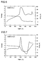
- the oxidation-start temperature stands for a minimum temperature at which both heat is absorbed accompanying the softening of the glass and heat is generated accompanying the oxidation of the metal on a TG-DTA curve, and the weight increases.
- the spacers 5 of the invention can be produced while reducing its tendency of being shrunk by firing, making it possible to effectively solve various problems caused by the shrinkage due to firing at the time when the spacers 5 are formed integrally with the face plate 2 or the back plate 3, e.g., effectively preventing the deformation of the spacers 5 and peeling the spacers 5 off from the face plate 2 or the back plate 3, and further making it possible to improve the positional precision of the spacers 5.
- the spacers 5 of the present invention can be produced while reducing the shrinkage due to firing, and are prevented from being deformed or peeled even when they have a height (not smaller than 500 ⁇ m) and a thickness (not larger than 200 ⁇ m) as described above, and can be precisely arranged maintaining a fine gap.
- the glass component may be a lead glass (PbO-B 2 O 3 -SiO 2 ), an alkali silicate glass, a bismuth glass (Bi 2 O 3 - B 2 O 3 ), a SiO 2 - B 2 O 3 glass, a soda glass or a silica glass.
- a lead glass containing PbO, SiO 2 and B 2 O 3 or a bismuth glass containing Bi 2 O 3 and B 2 O 3 from the standpoint of mechanical strength, sintering at a low temperature, wettability to the metal component, adhesiveness to the face plate 2 or the back plate 3 and chemical stability.
- the glass has a softening temperature usually over a range of from 370 to 850 °C. From the standpoint of producing the spacers 5 at a low temperature, however, it is most desired that the glass has a softening temperature of from 370 to 430 °C. Desirably, the glass is generally contained in the sintered product in an amount of from 40 to 75% by weight.
- the above-mentioned metal components i.e., Si, Zn, Al, Sn, Cu and Mg may be dispersed each alone in the sintered product or may be dispersed with two or more in combination in the sintered product.
- these metal components it is desired to use Si, Zn and Sn from the standpoint of imparting electrically conducting property, oxidation-start temperature and expansion of volume due to the oxidation of a metal. From the standpoint of compatibility to the glass and adhesiveness, further, it is most desired to use metallic Si.
- the oxides of Sn, Zn and Cu have relatively high electrically conducting property, and are desired from the standpoint of imparting electrically conducting property to the spacers 5.
- the above-mentioned metal component is contained in the sintered product in such an amount that the volume resistivity of the sintered product (spacer 5) is from 1 x 10 8 to 1 x 10 14 ⁇ cm at 25 °C.
- the volume resistivity is higher than the above range, it is not possible to effectively prevent the spacers 5 from being electrically charged.
- the volume resistivity is lower than the above range, on the other hand, it becomes difficult to obtain a densely sintered product, and the spacers 5 formed of such a sintered product are not satisfactory from the standpoint of strength.
- the content of the metal in the sintered product having such a volume resistivity is usually from 1.5 to 34% by weight though it may vary depending upon the kind of the metal.
- the sintered product constituting the spacers 5 of the present invention may further contain a ceramic filler such as TiO 2 , ZnO, SnO 2 , ZrO 2 , SiO 2 , BN or Al 2 O 3 in addition to the above-mentioned glass component and metal component.
- the ceramic filler works to lower the firing temperature, control the coefficient of thermal expansion of the sintered product, and to impart a color, and further works to adjust the distorting point of the glass so that the spacer 5 will not be deformed during the firing.
- the spacers 5 it is, for example, desired to so adjust the spacers 5 by using the ceramic filler that they exhibit an average coefficient of thermal expansion at 15 to 450 °C of from 7 to 9 ppm/°C and, particularly, from 7.5 to 8.2 ppm/°C.
- the face plate 2 or the back plate 3 provided with the spacers 5 having such an average coefficient of thermal expansion offers such an advantage that the spacers 5 do not develop such defect as cracking even when they are heated or cooled.
- the ceramic filler is used in an amount that will not impair the electrically conducting property imparted by the metal or will not impair the effect for reducing the shrinkage due to firing produced by the oxidation of the metal. It is desired that the content of the ceramic filler in the sintered product is not larger than 30% by weight and, particularly, not larger than 20% by weight.
- TiO 2 has a property of lowering the firing temperature and the oxidation-start temperature of the above-mentioned particular metal.
- the firing temperature can be lowered by not less than 10 °C, particularly, by not less than 20 °C and, more particularly, by not less than 30 °C.
- the rutile-type TiO 2 exhibits a property of more lowering the firing temperature than that of the anatase-type TiO 2 and exhibits a strong catalytic action for promoting the oxidation of a particular metal, but also exhibits a property of reducing the glass.
- the glass containing PbO and Bi 2 O 3 is used, in particular, it is advantageous to use ZnO or SnO 2 as the ceramic filler from the standpoint of obtaining a highly strong spacer. That is, when the mixture containing the above-mentioned glass and particular metal is fired, PbO and Bi 2 O 3 in the glass precipitate on the glass surfaces and are reduced accompanying the oxidation of the particular metal, permitting Pb and Bi to be evaporated and sublimated. As Pb and Bi evaporate and sublimate, many voids occur in the sintered product and, hence, the sintered product (spacer) loses the strength.
- the spacers 5 of the present invention formed of the above-mentioned sintered product are most suitably used for the picture display device 1 (FED) of the structure shown in Fig. 1.
- the spacers 5 of the present invention can be further preferably used for the picture display devices other than FED, such as plasma display panel (PDP) and plasma address liquid crystal panel (PALC) having a structure of which the interior is evacuated or is filled with a gas of a predetermined pressure.
- PDP plasma display panel
- PLC plasma address liquid crystal panel
- the ceramic for forming the spacers 5 suppresses the shrinkage caused by firing, and can be desirably used as an insulating plate for the wiring board equipped with a fine wiring layer, as a ferrule for connecting the optical fibers or optical parts, and as a sealing member.
- the spacers 5 of the invention are produced by preparing a molding paste containing a glass, the above-mentioned metal component and, as required, a ceramic filler, applying the paste onto a predetermined plate that forms the face plate 2 or the back plate 3, forming a molded article of spacers, and firing the molded article under predetermined conditions.
- the above-mentioned glass component in the sintered product for forming the spacers 5 is in the form of a powder having an average particle diameter of not larger than 6 ⁇ m from the standpoint of obtaining a densely sintered product.
- the above-mentioned metal for imparting electrically conducting property to the spacers 5 and for preventing the shrinking during the firing is in the form of a powder or a fiber having any shape such as spherical shape, irregular shape, hollow shape or flakes. It is further desired that the powder has an average particle size of from 0.5 to 6 ⁇ m and, particularly, from 1.0 to 3.0 ⁇ m from the standpoint of not oxidizing part of the metal by firing that will be described later, but leaving the metal to increase the surface areas of the metal to promote the expansion of volume by the oxidation of part of the metal. As described earlier, the metal component is used in such an amount that the volume resistivity (25 °C) of the sintered product lies within a predetermined range.
- the metal component is used in an amount of from 5 to 70 parts by weight and, particularly, from 20 to 60 parts by weight per 100 parts by weight of the glass powder.
- the amount of the metal is smaller than the above range, the effect for imparting electrically conducting property is not enough for preventing the electric charging, and the expansion of volume by oxidation is not enough for reducing the shrinkage caused by firing.
- the amount of the metal exceeds the above range, it becomes difficult not only to obtain a paste in which the metal is homogeneously dispersed but also to obtain a densely sintered product, and the strength of the spacers 5 may decrease.
- the ceramic filler used for adjusting the coefficient of thermal expansion has an average particle diameter of from 0.05 to 10 ⁇ m, preferably, from 0.1 to 3 ⁇ m and, most preferably, from 0.5 to 2 ⁇ m.
- the ceramic filler is used in an amount of not larger than 30% by weight and, particularly, not larger than 20% by weight in the sintered product.
- TiO 2 When TiO 2 is used as the ceramic filler, it is desired that its amount in the sintered product lies within the above-mentioned range, and is from 5 to 50 parts by weight per 100 parts by weight of the glass powder, and is from 16 to 600 parts by weight per 100 parts by weight of the above-mentioned particular metal.
- Use of the TiO 2 makes it possible to lower the firing temperature and the oxidation-start temperature of the particular metal, offering such an advantage that the phosphor layer 6 on the face plate 2 and the electron emissive elements 7 on the back plate 3 can be formed simultaneously with the spacers 5 by co-firing.
- the amount in the sintered product lies within the above-mentioned range, and is from 5 to 50 parts by weight per 100 parts by weight and, particularly, from 10 to 30 parts by weight per 100 parts by weight of the glass powder, and is from 10 to 150 parts by weight and, particularly, from 20 to 100 parts by weight per 100 parts by weight of the sum of PbO and Bi 2 O 3 in the glass.
- the molding paste is prepared by using the above-mentioned starting powder. That is, the above-mentioned glass powder, a powder of a particular metal and, as required, a ceramic filler are mixed together, and to which are added a binder such as acrylic resin, a plasticizer, a dispersant and an organic solvent, followed by kneading to prepare a molding paste in which the starting powders are homogeneously dispersed.
- a binder such as acrylic resin, a plasticizer, a dispersant and an organic solvent
- a molded article for spacers is formed on an insulating plate that serves as the face plate 2 or the back plate 3 by using the molding paste prepared above.
- Such molding can be carried out by print-applying the molding paste for molding onto the insulating plate plural times by using a mask such as predetermined pattern, or by arranging a mold on the insulating plate, filling the mold with the molding paste and removing the mold.
- a soft resin layer is formed on the insulating plate that serves as the face plate 2 or the back plate 3, recessed portions for forming spacers are engraved in the soft resin layer, the recessed portions for forming spacers are filled with the molding paste and, then, the soft resin layer is removed to form the molded article for spacers.
- an insulating plate 20 is prepared, and a soft resin layer 21 of a thickness corresponding to the height of the spacers 5 is formed on the insulating plate 20.
- the insulting plate 20 serves as the face plate 2 or the back plate 3 shown in Fig. 1, and is made of a glass or a ceramic.
- Recessed portions are easily formed in the soft resin layer 21 by press-molding that will be described later, the soft resin layer 21 being formed of a resin composition which maintains the recessed portions of a desired shape.
- the soft resin layer 21 is formed by applying a resin paste onto the insulating plate 20, the resin paste being obtained by mixing a resin component such as acrylic or butyral thermoplastic resin, an ultraviolet ray-curing resin, an electron ray-curing resin, a thermosetting resin or a wax with a plasticizer such as DBP (dibutyl phthalate), DOP (dioctyl phthalate) or ⁇ -terpineol, or a high-boiling solvent such as benzyl alcohol or IPA (isopropyl alcohol), so as to have a suitable softness.
- a resin component such as acrylic or butyral thermoplastic resin, an ultraviolet ray-curing resin, an electron ray-curing resin, a thermosetting resin or a wax
- a plasticizer such as
- a resin powder of a plastic cured in the form of beads may be added to the resin paste.
- the soft resin layer 21 is finally removed. Therefore, it is desired that the resin powder is completely decomposed and evaporated through the heat treatment at, for example, not higher than 600 °C.
- the resin paste can be easily applied by any known film-forming method, such as screen-printing method, doctor blade method, slit coater method, spin coater method, etc.
- an adhesive layer (not shown) may be formed maintaining a thickness of from about 1 to about 20 ⁇ m on the surface of the insulating plate 21.
- the resin component contained in the above-mentioned molding paste is blended in the adhesive layer to enhance the adhesiveness between the spacer 5 and the insulating plate 20 (face plate 2 or back plate 3).
- Recessed portions 23 for molding spacers are formed in the thus formed soft resin layer 21 by using a mold 22.
- the mold 22 has protrusions 22a corresponding to the shape of spacers.
- the mold 22 is pushed onto the soft resin layer 21 and is then pulled to form recessed portions 23.
- the mold 22 is made of a material having a high rigidity, such as metal, ceramics, glass or hardened resin, and is in the form of a flat plate or a roll.
- the mold 22 When the mold 22 is a flat plate, the mold 22 is arranged at a predetermined position on the surface of the soft resin layer 21, pushed with a predetermined pressure, and is pulled, to form recessed portions 23.
- the mold 22 When the mold 22 is a roll, the mold 22 is disposed at a predetermined position on the surface of the soft resin layer 21, rotated and moved while being pushed thereon, to form recessed portions 23.
- the recessed portions 23 for molding spacers are formed in the soft resin layer 21 which is, then cured, as required, to stabilize the shape of the recessed portions 23.
- the recessed portions 23 for molding spacers are formed as described above, it is desired that the recessed portions 23 have such a sectional shape that the width of the bottom is small and the width increases toward the upper portion as shown in Fig. 2d. That is, upon forming the recessed portions 23 in such a sectional shape, the metal mold 22 (protrusions 22a) can be easily pulled, and the spacers 5 have an increased strength as will be described later.
- the recessed portions 23 for forming spacers are filled with the above-mentioned molding paste (designated at 25 in Fig. 2e) for forming the spacers, thereby to mold the paste into the shape of spacers.
- the recessed portions 23 are filled with the molding paste by a known printing method such as screen-printing, packaging using a dispenser, vacuum injection, rubbing by squeezing, etc.
- the packaged molding paste is cured, as required, to stabilize the shape.
- the soft resin layer 21 is removed from the insulating plate 20 in a state where the recessed portions 23 are filled with the molding paste 25, thereby to obtain, as shown in Fig. 2f, a molded article of spacers (molded spacer articles) 26 on the insulating plate 20 that serves as the face plate 2 or the back plate 3.
- the soft resin layer 21 is removed by, for example,
- the thus molded spacer articles 26 have a shape corresponding to the recessed portions 23, i.e., have a spacer shape corresponding to the protrusions 22a formed on the mold 22, the width increasing toward the upper ends from the root portions thereof.
- the spacer articles 26 molded on the insulating plate 20 as described above are fired to obtain the spacers 5 firmly joined to the face plate 2 or to the back plate 3 integrally therewith.
- the firing must be conducted in an oxygen-containing atmosphere such as open air.
- an oxygen-containing atmosphere such as open air.
- a metal Si, Zn, Al, Sn, Cu or Mg contained in the molded spacer articles is partly oxidized to undergo the volume expansion reducing the shrinking caused by the sintering of glass in the molded articles, preventing the spacers 5 from being deformed by the shrinkage due to firing and effectively preventing the spacers 5 from being peeled off from the insulating plate 20 (face plate 2 or the back plate 3).
- the size difference is small between the molded spacer articles 26 and the spacers 5, i.e., a change in the size is as very small as 2% or less, particularly, 1% or less, more particularly, 0.5% or less and, further particularly, 0.3% or less.
- the firing it is desired to conduct the firing at a temperature of from 420 to 480 °C. Upon conducting the firing at such a temperature, it is allowed to obtain spacers 5 of a densely sintered product having a relative density of not smaller than 65%, preferably, not smaller than 70% and, most preferably, not smaller than 75%.
- the firing temperature is lower than the above range, the above-mentioned metal is not effectively oxidized and it becomes difficult to effectively relax the shrinkage caused by firing.
- the spacers 5 of the invention are formed on the insulating plate that serves as the face plate 2 or the back plate 3 integrally therewith, and exhibit a very high junction strength to the insulating plate. Due to the presence of the above-mentioned metal, further, the spacers 5 exhibit a highly electrically conducting property and a volume resistivity lying within the above-mentioned range, and are effectively prevented from being electrically charged.
- the spacers 5 of the present invention obtained as described above have a sectional shape as shown in Fig. 3a. That is, the spacers 5 have the sectional shape substantially the same as the molded spacer articles 26 shown in. Fig. 2f, i.e., have a trapezoidal shape in cross section, the width thereof increasing toward the ends thereof from the root portions thereof (side of the insulating plate 20). As will be obvious from Example 6 appearing later, the spacers 5 having the trapezoidal shape exhibit a very large strength against the load from the upper side.
- an angle ⁇ (hereinafter often called side surface angle) subtended by the side surface thereof and a perpendicular drawn to the surface of the insulating plate 20 on which the spacer 5 is integrally molded, lies over a range of from 0.5 to 8°.
- the trajectory of electrons emitted from the electron emissive element neighboring the spacer 5 is not hindered provided the angle (hereinafter often called inclination angle) ⁇ subtended by a straight line connecting the center of root of the spacer 5 to the center of upper end thereof and a perpendicular drawn to the surface of the insulating plate 20 is in a range of not larger than 5° as shown in Fig. 3b. That is, the spacer having a trapezoidal shape in cross section as shown in Fig. 3a maintains a large strength even when it is inclined as shown in Fig. 3b.
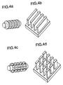
- the arrangement and shape of the thus formed spacers 5 are not limited to those of the rib shape, but may be arranged in various shapes such as lattices, poles and frames as shown in Figs. 4a to 4h.
- the spacers 5 are formed on the surface of the face plate 2 or the back plate 3 integrally therewith.
- the ends of the spacers 5 are adhered and secured in position on the back plate 3 or the face plate 2 with an adhesive such as frit glass to produce the picture display device of a structure shown in, for example, Fig. 1.
- the glass frit may be the one comprising the above-mentioned glass powder and a particular metal.
- the face plate 2 is obtained by preparing a transparent plate using the above-mentioned glass or the like, cutting it into a predetermined shape, forming an ITO film 10 and a black matrix 11 on one surface thereof, and forming a phosphor layer 6 on the portion surrounded by the black matrix 11.
- the ITO film 10 can be formed by a known printing method such as screen-printing method, gravure-printing method or offset printing method, by a paste-application method such as roll coater method, or by a deposition method.
- the black matrix 11 can be formed by a known printing method such as photolithography method, screen-printing method, gravure-printing method or offset printing method.
- the phosphor layer 6 can be formed by applying a phosphor paste by a printing method such as photolithography method, screen-printing method, gravure-printing method or offset printing method, or by an ink-jet method and, then, removing by evaporation the organic component in the phosphor paste by the heat treatment at 400 to 600 °C and, particularly, at 450 to 500 °C.
- a metal back is formed, as required, on the surface of the phosphor layer 6 by vaporization.
- the spacers 5 can be formed on the face plate 2 integrally therewith in any stage.
- the spacers 5 can be formed on the surface of the face plate 2 in a stage prior to forming the ITO film 10.
- the spacers 5 can be formed on the surface of the face plate 2 after the black matrix 11 and the phosphor layer 6 are formed.
- the spacers 5 and the phosphor layer 6 can be simultaneously formed by applying the phosphor paste onto predetermined positions after having formed the above-mentioned molded spacer articles 26, and firing the molded spacer articles 26 simultaneously with the heat treatment for removing the resin component from the phosphor paste.
- the back plate 3 is obtained by preparing a plate of the above-mentioned material, cutting the plate into a predetermined shape, forming a diffusion-preventing layer 12 on one surface of the plate and, then, forming electron emissive elements 7 comprising predetermined electrode layers 7a, 7b and insulating layers 7c.
- the diffusion-preventing layer 12 can be formed by sputtering method, CVD method, ion beam method, vaporization method or MBE method
- the electrode layers 7a, 7b can be formed by photolithography method
- the insulating layers 7c can be easily formed by a known thin film-forming method such as sputtering method, vaporization method, ion-beam method, CVD method and MBE method.
- a frame 4 for sealing the interior of the device is stuck with an adhesive such as frit glass onto the outer circumferential portion of either the thus formed face plate 2 or the back plate 3 (spacers 5 are integrally formed on either one of them). Thereafter, the face plate 2 and the back plate 3 are so positioned that the electron emissive elements 7 and the phosphor layer 6 face each other. Then, the ends of the spacers 5 and the upper end of the frame 4 are adhered and secured onto the face plate 2 or the back plate 3 with the frit glass or the like.
- an adhesive such as frit glass
- a gas discharge port 9 that has been formed in an end of the back plate 3 is connected to an external exhaust pipe, and the device is heated at 400 to 500 °C, while evacuating the interior of the device to a pressure of about 10 -4 Pa, to cure the adhesive. Finally, the gas discharge port 9 is sealed to produce the picture display device 1 having a structure shown in, for example, Fig. 1.
- TiO 2 was added as a ceramic filler in an amount of 30 parts by weight to 100 parts by weight of a low-melting glass of the type of PbO - B 2 O 3 - SiO 2 having a distorting point of 410 °C. Then, metal powders shown in Table 1 were added at ratios shown in Table 1 per 100 parts by weight of the above glass powder, and the mixtures were wet-mixed together by using a ball mill of zirconia balls in IPA (isopropyl alcohol) for 18 hours.
- IPA isopropyl alcohol
- the obtained molded spacer articles were measured for their thickness and height by using a laser displacement meter (LC-2440/2400 manufactured by Keyence Co.) to make sure that they possessed the same size as the silicone rubber mold within a measuring precision.
- a laser displacement meter LC-2440/2400 manufactured by Keyence Co.
- the silicone rubber mold possessed a depth of recessed portions (height of spacers) of 1200 ⁇ m, a width of recessed portions (thickness of spacers) of 200 ⁇ m, and a distance between the recessed portions (distance between the spacers) of 800 ⁇ m.
- the molded article was fired in an oxygen atmosphere (flowing oxygen at a flow rate of about 2 liters/min.) at 460 °C for 15 minutes. Then, the spacers were measured for their height using the same laser displacement meter as the one described above, and the ratio of the height of the spacers to the height of the molded article of spacers [ (height of spacers/height of molded article of spacers) x 100 % ] was calculated as a dimensional change.
- the appearance of the spacers was observed through a stereo microscope to judge the presence of peeling, warping, bending and cut.
- the spacers without them were regarded to be favorable as shown in Table 1.
- the spacers were partly pulverized and were measured by the X-ray diffraction to confirm the presence of the metal that was added. The presence of oxide of the metal was confirmed in all samples except the sample No. 1. Further, portions of the spacers were measured for their volume resistivities (described as resistance in the Table) by using an insulation tester. Sample No.
- samples Nos. 2 to 20 prepared according to the present invention shrunk little upon the firing of the spacers and were not peeled off the insulating plate.
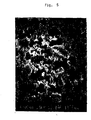
- the sample No. 6 was observed for its cross section using a scanning-type electron microscope (SEM) as shown in Fig. 5.
- SEM scanning-type electron microscope
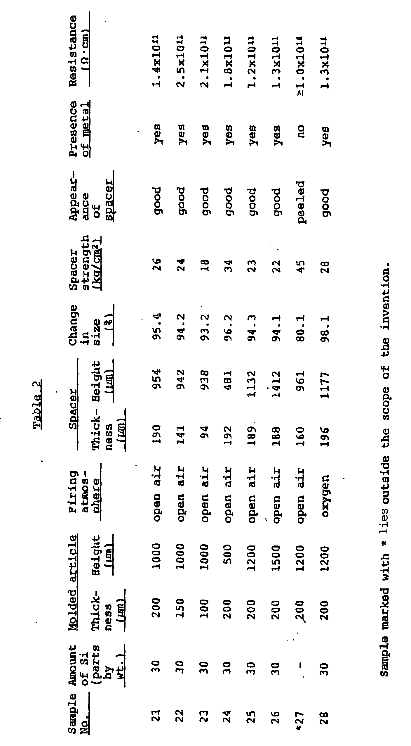
- the spacers were formed in the same manner as in Experiment 1 but changing the shape as shown in Table 2, and were evaluated for their shrinking factor upon firing and appearance. The results were as shown in Table 2. Samples Nos. 21 to 27 were fired in the open air.
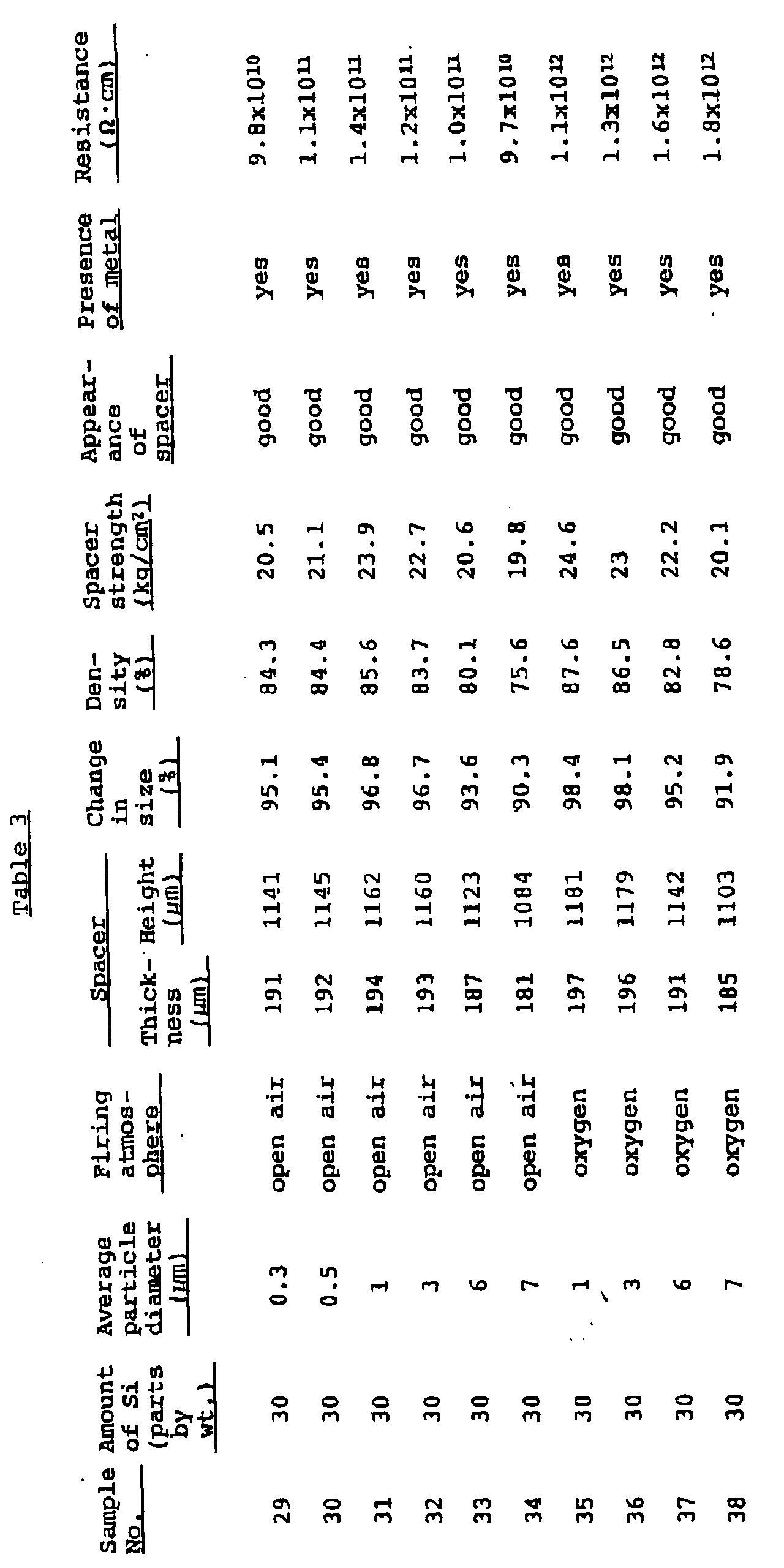
- the spacers were formed in the same manner as in Experiment 1 but adding metal powders having average particle diameters as shown in Table 3 and conducting the firing in the atmospheres shown in Table 3 to measure the change in the size and strength. Further, the spacer densities were measured by the helium gas substitution method to calculate relative densities which are ratios for the theoretical densities. The results were as shown in Table 3.
- samples No. 21 to 26 and 28 to 38 containing the metal Si in the sintered product according to the present invention made it possible to form spacers that were not deformed and that did not peel off, and further made it possible to impart electrically conducting property to the spacers.
- the samples Nos. 35 to 38 which were fired in oxygen exhibited further decreased change in the size.
- the change in the size could be further decreased with a decrease in the average particle diameter of the metal powder that was added.
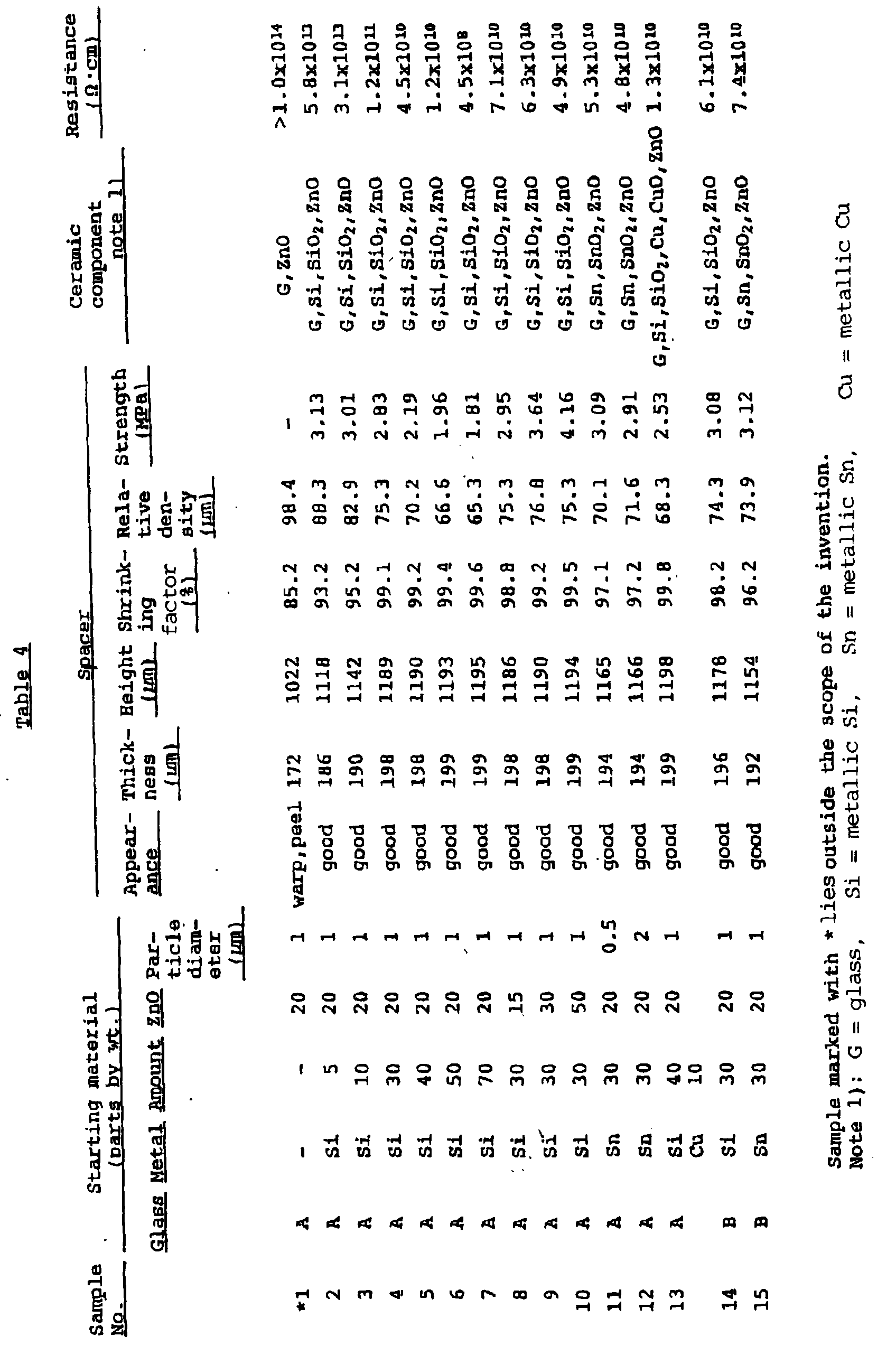
- the molded articles of spacers were formed in quite the same manner as in Experiment 1, and the molded articles were fired to prepare plates with spacers (the shapes of spacers and the firing conditions were the same as those of Experiment 1).
- samples Nos. 2 to 15, and 17 to 33, to which the predetermined metal and ZnO or SnO 2 were added according to the invention shrunk little upon the firing, and did not peeled off the insulating plate.
- the spacer strength could be increased to be not smaller than 1 MPa, particularly, not smaller than 1.5 MPa and, more particularly, not smaller than 2 MPa.
- a flat plate mold was prepared by forming 84 spacer protuberances maintaining a pitch of 600 ⁇ m on the surface of a flat metal plate measuring 50 x 50 x 5 mm, the protuberances having a width of 200 ⁇ m, a length of 50 mm and a height of 1000 ⁇ m.
- a silica layer was formed on the surface of the glass plate of a soda lime glass having a thickness of 2 mm and measuring 200 x 200 mm 2 .
- a plasticizer was added into a paraffin wax to prepare a resin paste.
- the resin paste was applied onto the silica layer of the glass plate using a slit coater to form a soft resin layer (1000 ⁇ m in thickness).
- the flat plate was pushed onto the soft resin layer on the glass plate to form recessed portions for forming spacers corresponding to the protuberances of the flat plate mold.
- the recessed portions for molding the spacers were filled with a paste for molding obtained by kneading a low-melting glass powder having an average particle diameter of 5 ⁇ m, an alumina powder, a metallic silicon powder, a binder, a solvent and a dispersant, followed by drying to solidify the paste. Thereafter, the glass plate was heated at 90 °C to flow out the resin layer.
- the glass plate from which the resin layer was removed was heated in open air to remove the binder, followed by firing at a temperature of 500 °C for 10 minutes to prepare spacers formed on the surface of the glass plate integrally therewith.
- the shape of the spacers formed on the plate was measured by using a laser displacement meter, and it was learned that the spacers had been formed having a height which is accurate to 1000 ⁇ 20 ⁇ m.
- a flat plate measuring 50 x 50 mm was placed on the plate with spacers, a force was exerted to compress the two plates in the direction of height of spacers to measure the load F at which the spacers were broken, and the pressure P (F/S) for the total area S of the spacers was calculated as a spacer strength.
- the spacer strength was 20 kg/cm 2 from which it was confirmed that the atmospheric pressure of 1 kg/cm 2 exerted on the spacers can be sufficiently coped with when the interior of the FED display panel is evacuated.
- a measurement of the resistance of the spacers indicated that the resistance of the spacers in which metallic silicon is remaining has dropped by more than 1, enabling the surfaces of the spacers to be less likely to be electrically charged.
- An ITO film was formed by vaporization on the surface of a glass plate of a soda lime having a thickness of 2 mm and measuring 40 x 40 mm to prepare a plate for a face plate.
- the recessed portions for molding the spacers were filled with the resin paste followed by drying to solidify the paste. Then, the plate was heated at 90 °C to dissolve the resin layer, thereby to form a molded article of spacers on the plate.
- the thus obtained plate with molded article of spacers was heated to remove the binder, followed by firing at 500 °C for 10 minutes to prepare a face plate on which the spacers were molded as a unitary structure.
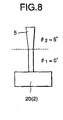
- the face plates having spacers molded as a unitary structure having a pitch of 700 ⁇ m, a height of 1200 ⁇ m, a width of 80 ⁇ m at the root portions, and having a width at the upper ends, a side surface angle ⁇ and an inclination angle ⁇ varying as shown in Table 6 (the side face angle ⁇ and the inclination angle ⁇ were measured by using a three-dimensional measuring instrument).
- the spacer of sample No. 7 has, as shown in Fig. 8, a side surface angle ⁇ of 0° on one-half side surface on the side of the root and has a side surface angle ⁇ of 5° on one-half side surface on the side of the upper end.
Landscapes
- Chemical & Material Sciences (AREA)
- Engineering & Computer Science (AREA)
- Chemical Kinetics & Catalysis (AREA)
- Ceramic Engineering (AREA)
- Dispersion Chemistry (AREA)
- Life Sciences & Earth Sciences (AREA)
- Manufacturing & Machinery (AREA)
- General Chemical & Material Sciences (AREA)
- Geochemistry & Mineralogy (AREA)
- Materials Engineering (AREA)
- Organic Chemistry (AREA)
- Cathode-Ray Tubes And Fluorescent Screens For Display (AREA)
- Vessels, Lead-In Wires, Accessory Apparatuses For Cathode-Ray Tubes (AREA)
Abstract
Description
| Sample No. | Metal | Spacer | Change in size (%) | Spacer strength (kg/cm2) | Appearance of spacer | Presence of metal | Resistance (Ω·cm) | ||
| Kind | Amount (parts by wt.) | Thickness (µm) | Height (µm) | ||||||
| *1 | - | - | 172 | 1022 | 85.2 | - | warped, peeled | no | ≥1.0x10¹⁴ |
| 2 | Si | 2 | 176 | 1051 | 87.6 | 10.2 | good | yes | 9.0x10¹³ |
| 3 | Si | 5 | 185 | 1108 | 92.3 | 27.8 | good | yes | 7.2x10¹³ |
| 4 | Si | 10 | 188 | 1129 | 94.1 | 27.3 | good | yes | 3.4x10¹³ |
| 5 | Si | 20 | 194 | 1162 | 96.8 | 25.2 | good | yes | 1.1x10¹³ |
| 6 | Si | 30 | 196 | 1177 | 98.1 | 23 | good | yes | 1.2x10¹¹ |
| 7 | Si | 45 | 197 | 1181 | 98.4 | 20.2 | good | yes | 2.8x10¹⁰ |
| 8 | Si | 50 | 198 | 1189 | 99.1 | 18.7 | good | yes | 1.7x10¹⁰ |
| 9 | Si | 60 | 198 | 1190 | 99.1 | 17.6 | good | yes | 3.4x10⁹ |
| 10 | Si | 70 | 199 | 1193 | 99.4 | 16.8 | good | yes | 4.8x10⁹ |
| 11 | Zn | 30 | 194 | 1162 | 96.8 | 24.6 | good | yes | 2.1x10¹⁰ |
| 12 | Al | 30 | 192 | 1151 | 95.9 | 25.3 | good | yes | 1.8x10¹⁰ |
| 13 | Cu | 30 | 198 | 1190 | 99.2 | 20.1 | good | yes | 6.2x10⁹ |
| 14 | Mg | 30 | 196 | 1175 | 97.9 | 23.8 | good | yes | 3.8x10¹⁰ |
| 15 | Sn | 30 | 192 | 1154 | 96.2 | 24.6 | good | yes | 1.9x10¹⁰ |
| 16 | Si | 2 | 179 | 1070 | 89.2 | 16.5 | good | yes | 4.9x10¹³ |
| Zn | 2 | ||||||||
| 17 | Si | 18 | 195 | 1168 | 97.3 | 26.3 | good | yes | 7.8x10¹⁰ |
| Zn | 13 | ||||||||
| 18 | Si | 20 | 198 | 1183 | 98.6 | 17.8 | good | yes | 2.4x10¹⁰ |
| Zn | 32 | ||||||||
| 19 | Si | 14 | 191 | 1147 | 95.6 | 22.7 | good | yes | 1.3x10¹⁰ |
| Al | 8 | ||||||||
| Cu | 4 | ||||||||
| 20 | Si | 17 | 199 | 1189 | 99.1 | 16.9 | good | yes | 6.2x10⁹ |
| Al | 16 | ||||||||
| Cu | 20 | ||||||||
| Sample marked with * lies outside the scope of the invention. |

| Sample No. | Width of upper end portion (µm) | Side surface angle (°) | Spacer strength (kg) | ||
| β = 0° | β = 6° | β = 8° | |||
| 1 | 80 | 0 | 1.2 | 0.25 | <0.1 |
| 2 | 100 | 0.5 | 1.3 | 0.65 | 0.15 |
| 3 | 160 | 2 | 1.1 | 0.82 | 0.31 |
| 4 | 240 | 4 | 1.5 | 1 | 0.65 |
| 5 | 420 | 8 | 1.3 | 0.95 | 0.8 |
| 6 | 500 | 10 | 1.4 | 1.3 | 1.2 |
| 7 | 180 | 0/5 | 1.2 | 0.56 | <0.1 |
| The width of spacers is 80 µm at the root. |
Claims (26)
- A spacer (5) disposed between a face plate (2) which displays a picture and a back plate (3) that faces a back surface of the face plate (2) to maintain space for electric discharge therebetween, characterized in that said spacer (5) is formed of a sintered product having a structure in which at least one kind of metal selected from the group consisting of Si, Zn, Al, Sn, Cu and Mg is dispersed in a glass.
- A spacer according to claim 1, wherein said glass contains PbO, SiO2 and B2O3.
- A spacer according to claim 1, wherein said glass contains Bi2O3 and B2O3.
- A spacer according to any of claims 1 to 3, wherein said sintered product further contains a filler.
- A spacer according to claim 4, wherein said filler is TiO2.
- A spacer according to claim 4, wherein said filler is ZnO or SnO2.
- A spacer according to any of claims 1 to 6, wherein said spacer has a volume resistivity of from 1 x 10⁸ to 1 x 10¹⁴ Ω cm (25 °C).
- A spacer according to any of claims 1 to 7, wherein said spacer has an average coefficient of linear thermal expansion (15 to 450 °C) of from 7 to 9 ppm/°C.
- A spacer according to any of claims 1 to 8, wherein said spacer has a thickness of not larger than 200 µm and a height of not smaller than 500 µm.
- A spacer according to any of claims 1 to 9, wherein said spacer is formed on the back surface of said face plate or on the surface of said back plate on the side of the face plate integrally therewith.
- A spacer according to any of claims 1 to 10, wherein the width of said spacer at the ends thereof is broader than the width at the root portions thereof.
- A spacer according to any of claims 1 to 11, wherein an angle subtended by the side surfaces of the spacer and a perpendicular drawn to the back surface of the face plate where said spacer is mounted or drawn onto the surface of the back plate on the side of the face plate, is from 0.5 to 8°.
- A method of producing a ceramic, characterized by preparing a molded article by using a mixture of a glass and at least one kind of metal selected from the group consisting of Si, Zn, Al, Sn, Cu and Mg, and firing the molded article in an oxygen-containing atmosphere to oxidize a part of said metal.
- A method of producing spacers according to claim 13, wherein said metal is in the form of a powder having an average particle diameter of not larger than 6 µm.
- A method of producing spacers according to claim 13 or 14, wherein said glass contains PbO, SiO2 and B2O3.
- A method of producing spacers according to claim 13 or 14, wherein said glass contains Bi2O3 and B2O3.
- A method of producing spacers according to any of claims 13 to 16, wherein said mixture of the glass and the metal further contains a filler.
- A method of producing spacers according to claim 17, wherein said filler is TiO2.
- A method of producing spacers according to claim 17, wherein said filler is ZnO or SnO2.
- A method of producing spacers, characterized by(a) a step of preparing a paste containing a glass and at least one kind of metal selected from the group consisting of Si, Zn, Al, Sn, Cu and Mg;(b) a step of forming a molded article of the spacers on the surface of a plate that serves as a face plate for displaying a picture or serves as a back plate by using said paste; and(c) a step of firing the molded article formed on the surface of said plate in an oxygen-containing atmosphere to oxidize part of said metal.
- A method of producing spacers according to claim 20, wherein said step (b) comprises:(b1) a step of forming a soft resin layer on the surface of said plate;(b2) a step of engraving recessed portions for molding spacers in the resin layer on the surface of said plate;(b3) a step of filling the recessed portions for molding said spacers with said paste to form said molded article; and(b4) a step of removing the resin layer from the surface of said plate.
- A method of producing spacers according to claim 20 or 21, wherein said resin layer is removed by a heat treatment or by a treatment with chemicals in said step (b4).
- A method of producing spacers according to any of claims 20 to 22, wherein said metal is used in an amount of from 5 to 50 parts by weight per 100 parts by weight of the glass.
- A picture display device, characterized by a face plate (2) for displaying a picture having a phosphor layer (6) formed on the back surface thereof, a back plate (3) facing a back surface of the face plate (2) and having electron emissive elements (7) on the surface thereof on the side of the face plate (2), and spacers (5) provided between the face plate (2) and the back plate (3) to maintain space for electric discharge therebetween, wherein said spacers (5) are formed of a sintered product having a structure in which at least one kind of metal selected from the group consisting of Si, Zn, Al, Sn, Cu and Mg is dispersed in a glass.
- A picture display device according to claim 24, wherein said spacers are formed in a plural number maintaining a suitable gap.
- A picture display device according to claim 24 or 25, wherein said spacers are formed on the back surface of said face plate integrally therewith, and the width of said spacers at the ends thereof are wider than the width of said spacers at the root portions therof.
Applications Claiming Priority (8)
| Application Number | Priority Date | Filing Date | Title |
|---|---|---|---|
| JP17160299 | 1999-06-17 | ||
| JP17160299 | 1999-06-17 | ||
| JP24535499A JP3758906B2 (en) | 1999-06-17 | 1999-08-31 | Substrate with spacer, flat display using the same, and method for manufacturing substrate with spacer |
| JP24535499 | 1999-08-31 | ||
| JP27535999A JP3898394B2 (en) | 1999-09-28 | 1999-09-28 | Manufacturing method of substrate with spacer |
| JP27535999 | 1999-09-28 | ||
| JP30964399 | 1999-10-29 | ||
| JP30964399A JP2001135263A (en) | 1999-10-29 | 1999-10-29 | Image forming apparatus and method of manufacturing the same |
Publications (3)
| Publication Number | Publication Date |
|---|---|
| EP1061546A2 true EP1061546A2 (en) | 2000-12-20 |
| EP1061546A3 EP1061546A3 (en) | 2001-04-25 |
| EP1061546B1 EP1061546B1 (en) | 2007-05-02 |
Family
ID=27474382
Family Applications (1)
| Application Number | Title | Priority Date | Filing Date |
|---|---|---|---|
| EP00112779A Expired - Lifetime EP1061546B1 (en) | 1999-06-17 | 2000-06-16 | Spacers used for picture display devices and a method of producing the same |
Country Status (3)
| Country | Link |
|---|---|
| US (1) | US6653769B1 (en) |
| EP (1) | EP1061546B1 (en) |
| DE (1) | DE60034629T2 (en) |
Cited By (1)
| Publication number | Priority date | Publication date | Assignee | Title |
|---|---|---|---|---|
| WO2001071760A1 (en) * | 2000-03-23 | 2001-09-27 | Kabushiki Kaisha Toshiba | Spacer assembly for plane surface display, method for manufacturing spacer assembly, method for manufacturing plane surface display, plane surface display and mold for use in manufacturing spacer assembly |
Families Citing this family (7)
| Publication number | Priority date | Publication date | Assignee | Title |
|---|---|---|---|---|
| US6791255B1 (en) * | 2002-09-04 | 2004-09-14 | Candescent Intellectual Property Services, Inc. | High coefficient of thermal expansion spacer structure materials |
| US7323232B2 (en) * | 2002-10-31 | 2008-01-29 | Fujifilm Corporation | Resin composition for spacer, spacer, and liquid crystal display device |
| TW200535901A (en) * | 2004-02-17 | 2005-11-01 | Tdk Corp | Method for producing spacer for flat panel display |
| KR20050104550A (en) * | 2004-04-29 | 2005-11-03 | 삼성에스디아이 주식회사 | Electron emission display device |
| JP2006054151A (en) * | 2004-08-16 | 2006-02-23 | Toshiba Corp | Image display device manufacturing method and image display device |
| CN100565758C (en) * | 2007-03-15 | 2009-12-02 | 东元电机股份有限公司 | Method for jointing support structure of field emission display assembly |
| WO2009069270A1 (en) * | 2007-11-27 | 2009-06-04 | Panasonic Corporation | Static electricity countermeasure component and method for manufacturing the static electricity countermeasure component |
Family Cites Families (13)
| Publication number | Priority date | Publication date | Assignee | Title |
|---|---|---|---|---|
| US3782407A (en) * | 1972-06-26 | 1974-01-01 | W Blackwell | Tap arrangement useful with measuring means |
| US4070517A (en) * | 1976-07-08 | 1978-01-24 | Beckman Instruments, Inc. | Low fired conductive compositions |
| JPS54150150A (en) * | 1978-05-17 | 1979-11-26 | Hitachi Ltd | Production of liquid crystal display element |
| US4255291A (en) * | 1979-06-21 | 1981-03-10 | E. I. Du Pont De Nemours And Company | Air-fireable conductor composition |
| US5675212A (en) * | 1992-04-10 | 1997-10-07 | Candescent Technologies Corporation | Spacer structures for use in flat panel displays and methods for forming same |
| JPH0682540B2 (en) * | 1986-06-27 | 1994-10-19 | 株式会社東芝 | Thick film resistance element and electron tube incorporating the same |
| JPH06310043A (en) * | 1992-08-25 | 1994-11-04 | Sharp Corp | Electron emission device |
| JP3365072B2 (en) * | 1994-09-19 | 2003-01-08 | 松下電器産業株式会社 | Ferrite material and method for producing the same |
| JP3806768B2 (en) * | 1997-03-28 | 2006-08-09 | 東レ株式会社 | Method for manufacturing plasma display panel |
| US6200181B1 (en) * | 1997-07-01 | 2001-03-13 | Candescent Technologies Corporation | Thermally conductive spacer materials and spacer attachment methods for thin cathode ray tube |
| US6366014B1 (en) * | 1997-08-01 | 2002-04-02 | Canon Kabushiki Kaisha | Charge-up suppressing member, charge-up suppressing film, electron beam apparatus, and image forming apparatus |
| JPH1173874A (en) * | 1997-09-01 | 1999-03-16 | Toray Ind Inc | Manufacturing method of plasma display |
| US6387600B1 (en) * | 1999-08-25 | 2002-05-14 | Micron Technology, Inc. | Protective layer during lithography and etch |
-
2000
- 2000-06-16 DE DE60034629T patent/DE60034629T2/en not_active Expired - Lifetime
- 2000-06-16 US US09/595,979 patent/US6653769B1/en not_active Expired - Fee Related
- 2000-06-16 EP EP00112779A patent/EP1061546B1/en not_active Expired - Lifetime
Cited By (3)
| Publication number | Priority date | Publication date | Assignee | Title |
|---|---|---|---|---|
| WO2001071760A1 (en) * | 2000-03-23 | 2001-09-27 | Kabushiki Kaisha Toshiba | Spacer assembly for plane surface display, method for manufacturing spacer assembly, method for manufacturing plane surface display, plane surface display and mold for use in manufacturing spacer assembly |
| US6583549B2 (en) | 2000-03-23 | 2003-06-24 | Kabushiki Kaisha Toshiba | Spacer assembly for flat panel display apparatus, method of manufacturing spacer assembly, method of manufacturing flat panel display apparatus, flat panel display apparatus, and mold used in manufacture of spacer assembly |
| US6672927B2 (en) | 2000-03-23 | 2004-01-06 | Kabushiki Kaisha Toshiba | Laminated mold for spacer assembly of a flat panel display |
Also Published As
| Publication number | Publication date |
|---|---|
| US6653769B1 (en) | 2003-11-25 |
| DE60034629T2 (en) | 2008-01-31 |
| DE60034629D1 (en) | 2007-06-14 |
| EP1061546A3 (en) | 2001-04-25 |
| EP1061546B1 (en) | 2007-05-02 |
Similar Documents
| Publication | Publication Date | Title |
|---|---|---|
| US6489718B1 (en) | Spacer suitable for use in flat panel display | |
| US5674634A (en) | Insulator composition, green tape, and method for forming plasma display apparatus barrier-rib | |
| KR20010053545A (en) | Embossed plasma display back panel | |
| EP1061546B1 (en) | Spacers used for picture display devices and a method of producing the same | |
| JP2004238247A (en) | Glass ceramic composition and thick film glass paste composition | |
| EP0722179A2 (en) | Insulator composition, green tape, and method for forming plasma display apparatus barrier-rib | |
| JP2001338528A (en) | Conductive frit for sealing and sealing member using the same as well as image forming device | |
| JP2009062524A (en) | Conductive ink for offset printing and method for producing electrode substrate for plasma display panel using the conductive ink | |
| JP3999942B2 (en) | SUBSTRATE WITH PROJECT MEMBER, ITS MANUFACTURING METHOD, AND IMAGE FORMING APPARATUS | |
| JP5060722B2 (en) | Composition for forming electron emission source and method for forming coating film for electron emission source | |
| JP3878792B2 (en) | Protruded substrate, method of manufacturing the same, and flat display | |
| JP3878790B2 (en) | Protruded substrate and method for manufacturing the same, flat display and method for manufacturing the same | |
| JP2004172250A (en) | Thick film resistor composition, thick film resistor using the same, and method of forming the same | |
| JP2001283721A (en) | Substrate with projection and flat panel display | |
| JP3758906B2 (en) | Substrate with spacer, flat display using the same, and method for manufacturing substrate with spacer | |
| JP3878958B2 (en) | Porcelain composition | |
| US20070024171A1 (en) | Spacer for planar panel display, process for producing the same and planar panel display | |
| JP4041271B2 (en) | Protruded substrate and flat display using the same | |
| JP3898394B2 (en) | Manufacturing method of substrate with spacer | |
| JP2006124277A (en) | Porcelain composition, porcelain and method for producing porcelain | |
| JP4518661B2 (en) | Manufacturing method of image display device | |
| JP2002075252A (en) | Coated particles, substrate with projections using the same, and flat display | |
| JP2008214144A (en) | Dielectric composition and dielectric and dielectric paste using the dielectric composition | |
| JP2002075253A (en) | Front plate for flat display and flat display using the same | |
| KR20060116117A (en) | Manufacturing Method of Plasma Display Panel |
Legal Events
| Date | Code | Title | Description |
|---|---|---|---|
| PUAI | Public reference made under article 153(3) epc to a published international application that has entered the european phase |
Free format text: ORIGINAL CODE: 0009012 |
|
| AK | Designated contracting states |
Kind code of ref document: A2 Designated state(s): DE FR |
|
| AX | Request for extension of the european patent |
Free format text: AL;LT;LV;MK;RO;SI |
|
| RIN1 | Information on inventor provided before grant (corrected) |
Inventor name: KATO, MASASHI, C/O KYOCERA CORPORATION Inventor name: SAKASEGAWA, KIYOHIRO, C/O KYOCERA CORPORATION Inventor name: MURAMOTO, YASUHITO, C/O KYOCERA CORPORATION Inventor name: NISHIOKA, YASUHIKO, C/O KYOCERA CORPORATION Inventor name: WATADA, KAZUO, C/O KYOCERA CORPORATION Inventor name: TAKAHASHI, AKIHIKO, C/O KYOCERA CORPORATION Inventor name: HAMADA, KOUJI, C/O KYOCERA CORPORATION |
|
| PUAL | Search report despatched |
Free format text: ORIGINAL CODE: 0009013 |
|
| AK | Designated contracting states |
Kind code of ref document: A3 Designated state(s): AT BE CH CY DE DK ES FI FR GB GR IE IT LI LU MC NL PT SE |
|
| AX | Request for extension of the european patent |
Free format text: AL;LT;LV;MK;RO;SI |
|
| 17P | Request for examination filed |
Effective date: 20011022 |
|
| AKX | Designation fees paid |
Free format text: DE FR |
|
| GRAP | Despatch of communication of intention to grant a patent |
Free format text: ORIGINAL CODE: EPIDOSNIGR1 |
|
| GRAS | Grant fee paid |
Free format text: ORIGINAL CODE: EPIDOSNIGR3 |
|
| GRAA | (expected) grant |
Free format text: ORIGINAL CODE: 0009210 |
|
| AK | Designated contracting states |
Kind code of ref document: B1 Designated state(s): DE FR |
|
| REF | Corresponds to: |
Ref document number: 60034629 Country of ref document: DE Date of ref document: 20070614 Kind code of ref document: P |
|
| ET | Fr: translation filed | ||
| PLBE | No opposition filed within time limit |
Free format text: ORIGINAL CODE: 0009261 |
|
| STAA | Information on the status of an ep patent application or granted ep patent |
Free format text: STATUS: NO OPPOSITION FILED WITHIN TIME LIMIT |
|
| 26N | No opposition filed |
Effective date: 20080205 |
|
| REG | Reference to a national code |
Ref country code: FR Ref legal event code: TP |
|
| PGFP | Annual fee paid to national office [announced via postgrant information from national office to epo] |
Ref country code: DE Payment date: 20140513 Year of fee payment: 15 Ref country code: FR Payment date: 20140513 Year of fee payment: 15 |
|
| REG | Reference to a national code |
Ref country code: DE Ref legal event code: R119 Ref document number: 60034629 Country of ref document: DE |
|
| REG | Reference to a national code |
Ref country code: FR Ref legal event code: ST Effective date: 20160229 |
|
| PG25 | Lapsed in a contracting state [announced via postgrant information from national office to epo] |
Ref country code: DE Free format text: LAPSE BECAUSE OF NON-PAYMENT OF DUE FEES Effective date: 20160101 |
|
| PG25 | Lapsed in a contracting state [announced via postgrant information from national office to epo] |
Ref country code: FR Free format text: LAPSE BECAUSE OF NON-PAYMENT OF DUE FEES Effective date: 20150630 |