EP1061427B1 - Controlled current, voltage mode driving stage - Google Patents
Controlled current, voltage mode driving stage Download PDFInfo
- Publication number
- EP1061427B1 EP1061427B1 EP99830369A EP99830369A EP1061427B1 EP 1061427 B1 EP1061427 B1 EP 1061427B1 EP 99830369 A EP99830369 A EP 99830369A EP 99830369 A EP99830369 A EP 99830369A EP 1061427 B1 EP1061427 B1 EP 1061427B1
- Authority
- EP
- European Patent Office
- Prior art keywords
- current
- node
- load
- transistor
- coupled
- Prior art date
- Legal status (The legal status is an assumption and is not a legal conclusion. Google has not performed a legal analysis and makes no representation as to the accuracy of the status listed.)
- Expired - Lifetime
Links
- 238000000034 method Methods 0.000 claims description 7
- 230000000295 complement effect Effects 0.000 claims description 5
- 230000009977 dual effect Effects 0.000 description 3
- 230000010354 integration Effects 0.000 description 2
- XUIMIQQOPSSXEZ-UHFFFAOYSA-N Silicon Chemical compound [Si] XUIMIQQOPSSXEZ-UHFFFAOYSA-N 0.000 description 1
- 230000001419 dependent effect Effects 0.000 description 1
- 238000004519 manufacturing process Methods 0.000 description 1
- 238000012544 monitoring process Methods 0.000 description 1
- 229910052710 silicon Inorganic materials 0.000 description 1
- 239000010703 silicon Substances 0.000 description 1
Images


Classifications
-
- H—ELECTRICITY
- H03—ELECTRONIC CIRCUITRY
- H03F—AMPLIFIERS
- H03F3/00—Amplifiers with only discharge tubes or only semiconductor devices as amplifying elements
- H03F3/30—Single-ended push-pull [SEPP] amplifiers; Phase-splitters therefor
- H03F3/3069—Single-ended push-pull [SEPP] amplifiers; Phase-splitters therefor the emitters of complementary power transistors being connected to the output
- H03F3/3071—Single-ended push-pull [SEPP] amplifiers; Phase-splitters therefor the emitters of complementary power transistors being connected to the output with asymmetrical driving of the end stage
-
- H—ELECTRICITY
- H03—ELECTRONIC CIRCUITRY
- H03F—AMPLIFIERS
- H03F1/00—Details of amplifiers with only discharge tubes, only semiconductor devices or only unspecified devices as amplifying elements
- H03F1/52—Circuit arrangements for protecting such amplifiers
-
- H—ELECTRICITY
- H03—ELECTRONIC CIRCUITRY
- H03F—AMPLIFIERS
- H03F3/00—Amplifiers with only discharge tubes or only semiconductor devices as amplifying elements
- H03F3/50—Amplifiers in which input is applied to, or output is derived from, an impedance common to input and output circuits of the amplifying element, e.g. cathode follower
Definitions
- the invention relates to integrated circuits and in particular output power stages.
- the invention concerns a method and relative implementing stage for driving with a controlled current a load.
- the invention relates to an output stage that is able to drive in a voltage mode a load and which is current controlled, such that the driving of the load is normally performed in a voltage mode one and whenever the load requires a particularly high current, the driving is performed in a current mode.
- a voltage mode driving from node A to node B, which becomes automatically a current mode driving whenever the load requires a current greater than Hfe*Iin (where Hfe is the current gain of the transistor T1).
- the input variables of the circuit are the voltage produced on the A node by the circuit that precedes the output stage (not illustrated in figure) and the current Iin, injected by the circuit preceding the output stage.
- the known solution is disadvantageous because the output current depends to a significant extent the parameters of the manufacturing process and temperature, besides the level of the signal itself, but not linearly because of the variability of the Hfe parameter of the transistor of the output stage depending from the collector current.
- the circuit of the known solution may develop output voltages below ground and above the supply voltage. It is able to drive only loads referred (connected) to ground, and to be able to deliver and to absorb current it must be associated to a correspondent dual structure.
- US-A-4,599,578 discloses a method for applying a driving voltage to a load using a bipolar junction drive transistor by measuring the load current on the emitter side of the transistor, generating a measured output current proportional to the load current generating a current different by comparing the measured output current with a reference current and injecting a current proportional to the current difference into the base of the bipolar drive transistor.
- US-A-4,258,406 discloses a circuit for protecting output transistors of a push-pull output amplifier based on detecting the collector current or the emitter current of the transistor to be protected on a current sensing resistor and applying the detected signal to a control transistor via an emitter-collector path of a transistor having a register connected across the collector and the base.
- An object of the invention is to provide an improved driving method and an output stage that couples low voltage drop and wide range of operating voltage characteristics (from below ground values to above supply values) with those of an improved current control with relatively small input currents, being less dependent from process spread and from temperature, irrespectively of the level of the input voltage signal.
- the method of voltage driving with controlled current of the invention consists in realizing a negative feedback of the output current, measured on the collector of the transistor of the output stage, in comparing the current measured at the transistor collector with the input current and injecting the current difference in the base of the transistor on which node the voltage driving assures.
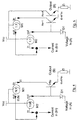
- Figure 1 is a basic scheme of an output stage for voltage driving with a current controlled, a load according to a known technique, as discussed above.
- Figure 2 shows the basic circuit of a known output stage, according to the scheme of Fig. 1.
- Figure 3 shows the basic circuit of a fully complementary output stage, made according to the present invention.
- Figure 3a shows a basic circuit of a unipolar stage of the invention, capable only of delivering current to a load.
- Figure 3b shows a dual version of the circuit of Fig. 3a, capable of driving a load referred to the positive supply rail instead of to ground.
- Figure 4 shows an alternative embodiment of an output stage according to the present invention.
- Figure 5 shows another alternative embodiment of an output stage according to the present invention.
- the circuit of Fig. 2 represents an embodiment of a fully complementary stage as often preferred in order to maximize the efficiency and the output voltage swing.
- the diode D 1 results turned on, thus enabling the voltage driving of the base of the output transistor T1. Therefore, the load is driven in voltage mode.
- the excess current on the base node of the transistor is absorbed by the circuit that precedes the voltage input node A of the output stage.
- Fig. 3b The scheme of Fig. 3b is functionally similar to the scheme of Fig. 3a. It represents the dual version of the circuit of Fig. 3a, for driving a load referred to the positive supply voltage node instead of to ground.
- FIG. 5 yet another alternative embodiment of the circuit of the invention is shown in Fig. 5.
- the purpose of this alternative scheme is to save integration area by realizing the feedback loop with a current mirror M1 that does not have to monitor necessarily the whole collector current of the output transistor of the stage, but just a fractional current of the collector, read on a suitably scaled structure of the output transistor.
- the feedback current mirror is typically realized with PNP transistors, this expedient allows a considerable saving of integration area.
Landscapes
- Engineering & Computer Science (AREA)
- Power Engineering (AREA)
- Amplifiers (AREA)
Description
Claims (6)
- A method of voltage driving with a controlled current a load (Z1) referred to ground or to a supply voltage (Vcc) using a stage including at least a transistor (T1), with an emitter coupled to the load (Z1) and a collector coupled to the supply node opposite the one to which the load (Z1) is referred and at least a first current mirror (M2) whose input (IN) is coupled to a source of an input current (Iin) and whose output (OUT) is coupled to the base of the transistor (T1) and through a directly biased diode (D1) to a node (A) coupled to a source of an input voltage (Vin), characterized by the steps of
mirroring the collector current of said transistor (T1) by a second current mirror (M1) referred to said supply node opposite to the node to which the load is referred and comparing said input current (Iin) with the collector current mirrored by said second mirror (M1) on a circuit node;
injecting or absorbing from said circuit node a current difference of said comparison through said first current mirror (M2) on or from the base node of said transistor (T1) or forcing or absorbing said current difference through said diode (D1) to or from a circuit preceding the stage for producing on said node (A) said input voltage (Vin). - A stage for voltage driving with a controlled current a load (Z1) referred to ground or to a supply voltage (Vcc), comprising at least a transistor (T1), having an emitter coupled to the load (Z1) and a collector coupled to the supply node opposite the one to which the load (Z1) is referred, at least a first current mirror (M2) whose input (IN) is coupled to a source of an input current (Iin) and whose output (OUT) is coupled to the base of the transistor (T1) and by a directly biased diode (D1) to a node (A) coupled to a source of an input voltage (Vin), characterized in that
the collector of said transistor (T1) is coupled to the input of a second current mirror (M1), referred to said supply node opposite to the node to which the load is referred, the output of said second current mirror (M1) is coupled to a node on which said input current (Iin) and the collector current mirrored by said second current mirror (M1) are compared, the first current mirror (M2) injecting or absorbing a current difference of said comparison on or from the base node of said transistor (T1) or forcing or absorbing said current difference through said diode (D1) to or from a circuit preceding said stage and producing upon said node (A) said input voltage (Vin). - The stage according to claim 2, characterized in that said second current mirror (M1) has a mirroring ratio smaller than 1.
- The stage according to claim 2, characterized in that said first current mirror (M2) has a mirroring ratio greater than 1.
- The stage according to claim 2, characterized in that said second current mirror (M1) mirrors a fraction of the collector current of said transistor (T1) of the stage.
- The stage according to any claim from 2 to 5, characterized in that is realized in a complementary form.
Priority Applications (3)
| Application Number | Priority Date | Filing Date | Title |
|---|---|---|---|
| EP99830369A EP1061427B1 (en) | 1999-06-15 | 1999-06-15 | Controlled current, voltage mode driving stage |
| DE69902889T DE69902889D1 (en) | 1999-06-15 | 1999-06-15 | Voltage controlled driver stage with regulated current |
| US09/594,244 US6392393B1 (en) | 1999-06-15 | 2000-06-15 | Controlled current, voltage mode driving stage |
Applications Claiming Priority (1)
| Application Number | Priority Date | Filing Date | Title |
|---|---|---|---|
| EP99830369A EP1061427B1 (en) | 1999-06-15 | 1999-06-15 | Controlled current, voltage mode driving stage |
Publications (2)
| Publication Number | Publication Date |
|---|---|
| EP1061427A1 EP1061427A1 (en) | 2000-12-20 |
| EP1061427B1 true EP1061427B1 (en) | 2002-09-11 |
Family
ID=8243450
Family Applications (1)
| Application Number | Title | Priority Date | Filing Date |
|---|---|---|---|
| EP99830369A Expired - Lifetime EP1061427B1 (en) | 1999-06-15 | 1999-06-15 | Controlled current, voltage mode driving stage |
Country Status (3)
| Country | Link |
|---|---|
| US (1) | US6392393B1 (en) |
| EP (1) | EP1061427B1 (en) |
| DE (1) | DE69902889D1 (en) |
Families Citing this family (3)
| Publication number | Priority date | Publication date | Assignee | Title |
|---|---|---|---|---|
| US6043562A (en) * | 1996-01-26 | 2000-03-28 | Micron Technology, Inc. | Digit line architecture for dynamic memory |
| US7221766B2 (en) | 2002-04-15 | 2007-05-22 | Knowles Electronics, Llc | Microphone input buffer biasing circuit |
| EP1496613A1 (en) * | 2003-07-09 | 2005-01-12 | C.S.E.M. Centre Suisse D'electronique Et De Microtechnique Sa | Source follower circuit |
Family Cites Families (7)
| Publication number | Priority date | Publication date | Assignee | Title |
|---|---|---|---|---|
| JPS5510208A (en) * | 1978-07-07 | 1980-01-24 | Hitachi Ltd | Aso protection circuit |
| NL8302197A (en) * | 1983-06-21 | 1985-01-16 | Philips Nv | SECURITY CIRCUIT. |
| US5084668A (en) * | 1990-06-08 | 1992-01-28 | Motorola, Inc. | System for sensing and/or controlling the level of current in a transistor |
| US5225766A (en) * | 1991-01-04 | 1993-07-06 | The Perkin Elmer Corporation | High impedance current source |
| DE19710440A1 (en) * | 1997-03-13 | 1998-09-24 | Bosch Gmbh Robert | Power supply circuit |
| JP3697679B2 (en) * | 1997-09-25 | 2005-09-21 | ローム株式会社 | Stabilized power circuit |
| JPH11154835A (en) * | 1997-11-21 | 1999-06-08 | Seiko Instruments Inc | Differential amplifier |
-
1999
- 1999-06-15 DE DE69902889T patent/DE69902889D1/en not_active Expired - Lifetime
- 1999-06-15 EP EP99830369A patent/EP1061427B1/en not_active Expired - Lifetime
-
2000
- 2000-06-15 US US09/594,244 patent/US6392393B1/en not_active Expired - Lifetime
Also Published As
| Publication number | Publication date |
|---|---|
| EP1061427A1 (en) | 2000-12-20 |
| DE69902889D1 (en) | 2002-10-17 |
| US6392393B1 (en) | 2002-05-21 |
Similar Documents
| Publication | Publication Date | Title |
|---|---|---|
| US20090273874A1 (en) | Power switch circuit exhibiting over current and short circuit protection and method for limiting the output current thereof | |
| US6507227B2 (en) | Device and method for monitoring current delivered to a load | |
| JP2000252804A (en) | Overcurrent detection circuit and semiconductor integrated circuit incorporating the same | |
| US20030086456A1 (en) | Laser drive device | |
| EP0789452B1 (en) | A power amplifier with bootstrap voltage clamp | |
| EP1061427A1 (en) | Controlled current, voltage mode driving stage | |
| JP3959924B2 (en) | Load drive circuit | |
| JP2876522B2 (en) | IC with built-in overvoltage detection circuit | |
| US6605967B2 (en) | Low power consumption output driver circuit and supply voltage detection circuit | |
| KR100405372B1 (en) | Automatic gain control circuit | |
| JP3380308B2 (en) | Optical semiconductor relay device | |
| JP2604497B2 (en) | Multiple output power supply circuit | |
| JP3094653B2 (en) | Overcurrent protection circuit | |
| JP2623954B2 (en) | Variable gain amplifier | |
| JP3063345B2 (en) | Saturation prevention circuit | |
| EP1127407A1 (en) | An amplifier for use in a mobile phone | |
| KR200247759Y1 (en) | Automatic gain control circuit | |
| JPH0749541Y2 (en) | Transistor switch circuit | |
| JPH0218772B2 (en) | ||
| JP3043247B2 (en) | Photo detector | |
| JP3035921B2 (en) | High frequency power amplifier | |
| JPH0749853Y2 (en) | Malfunction prevention circuit for differential amplifier | |
| KR930008346Y1 (en) | Automatic Gain Control Circuit with Extended Control Range | |
| JP2591805Y2 (en) | Power supply voltage monitoring circuit | |
| KR0132407Y1 (en) | Power source voltage reduction detection circuit |
Legal Events
| Date | Code | Title | Description |
|---|---|---|---|
| PUAI | Public reference made under article 153(3) epc to a published international application that has entered the european phase |
Free format text: ORIGINAL CODE: 0009012 |
|
| AK | Designated contracting states |
Kind code of ref document: A1 Designated state(s): DE FR GB IT |
|
| AX | Request for extension of the european patent |
Free format text: AL;LT;LV;MK;RO;SI |
|
| 17P | Request for examination filed |
Effective date: 20010118 |
|
| 17Q | First examination report despatched |
Effective date: 20010710 |
|
| AKX | Designation fees paid |
Free format text: DE FR GB IT |
|
| GRAG | Despatch of communication of intention to grant |
Free format text: ORIGINAL CODE: EPIDOS AGRA |
|
| GRAG | Despatch of communication of intention to grant |
Free format text: ORIGINAL CODE: EPIDOS AGRA |
|
| GRAH | Despatch of communication of intention to grant a patent |
Free format text: ORIGINAL CODE: EPIDOS IGRA |
|
| GRAH | Despatch of communication of intention to grant a patent |
Free format text: ORIGINAL CODE: EPIDOS IGRA |
|
| GRAA | (expected) grant |
Free format text: ORIGINAL CODE: 0009210 |
|
| AK | Designated contracting states |
Kind code of ref document: B1 Designated state(s): DE FR GB IT |
|
| PG25 | Lapsed in a contracting state [announced via postgrant information from national office to epo] |
Ref country code: FR Free format text: LAPSE BECAUSE OF NON-PAYMENT OF DUE FEES Effective date: 20020911 |
|
| REG | Reference to a national code |
Ref country code: GB Ref legal event code: FG4D |
|
| REF | Corresponds to: |
Ref document number: 69902889 Country of ref document: DE Date of ref document: 20021017 |
|
| PG25 | Lapsed in a contracting state [announced via postgrant information from national office to epo] |
Ref country code: DE Free format text: LAPSE BECAUSE OF FAILURE TO SUBMIT A TRANSLATION OF THE DESCRIPTION OR TO PAY THE FEE WITHIN THE PRESCRIBED TIME-LIMIT Effective date: 20021212 |
|
| EN | Fr: translation not filed | ||
| PLBE | No opposition filed within time limit |
Free format text: ORIGINAL CODE: 0009261 |
|
| STAA | Information on the status of an ep patent application or granted ep patent |
Free format text: STATUS: NO OPPOSITION FILED WITHIN TIME LIMIT |
|
| 26N | No opposition filed |
Effective date: 20030612 |
|
| PGFP | Annual fee paid to national office [announced via postgrant information from national office to epo] |
Ref country code: GB Payment date: 20070530 Year of fee payment: 9 |
|
| PGFP | Annual fee paid to national office [announced via postgrant information from national office to epo] |
Ref country code: IT Payment date: 20070607 Year of fee payment: 9 |
|
| GBPC | Gb: european patent ceased through non-payment of renewal fee |
Effective date: 20080615 |
|
| PG25 | Lapsed in a contracting state [announced via postgrant information from national office to epo] |
Ref country code: GB Free format text: LAPSE BECAUSE OF NON-PAYMENT OF DUE FEES Effective date: 20080615 |
|
| PG25 | Lapsed in a contracting state [announced via postgrant information from national office to epo] |
Ref country code: IT Free format text: LAPSE BECAUSE OF NON-PAYMENT OF DUE FEES Effective date: 20080615 |