EP1060344B1 - A lenticular illumination system - Google Patents
A lenticular illumination system Download PDFInfo
- Publication number
- EP1060344B1 EP1060344B1 EP99911043A EP99911043A EP1060344B1 EP 1060344 B1 EP1060344 B1 EP 1060344B1 EP 99911043 A EP99911043 A EP 99911043A EP 99911043 A EP99911043 A EP 99911043A EP 1060344 B1 EP1060344 B1 EP 1060344B1
- Authority
- EP
- European Patent Office
- Prior art keywords
- light
- waveguide
- microprism
- microprisms
- input surface
- Prior art date
- Legal status (The legal status is an assumption and is not a legal conclusion. Google has not performed a legal analysis and makes no representation as to the accuracy of the status listed.)
- Expired - Lifetime
Links
- 238000005286 illumination Methods 0.000 title claims description 16
- 230000003287 optical effect Effects 0.000 claims description 13
- 239000000463 material Substances 0.000 description 16
- 239000010410 layer Substances 0.000 description 15
- 238000000034 method Methods 0.000 description 8
- 125000006850 spacer group Chemical group 0.000 description 7
- 239000011800 void material Substances 0.000 description 6
- NIXOWILDQLNWCW-UHFFFAOYSA-N acrylic acid group Chemical group C(C=C)(=O)O NIXOWILDQLNWCW-UHFFFAOYSA-N 0.000 description 5
- 238000009826 distribution Methods 0.000 description 5
- 229920001296 polysiloxane Polymers 0.000 description 5
- 239000004793 Polystyrene Substances 0.000 description 4
- 239000011521 glass Substances 0.000 description 4
- 238000004519 manufacturing process Methods 0.000 description 4
- 229920000642 polymer Polymers 0.000 description 4
- 229920002223 polystyrene Polymers 0.000 description 4
- 239000004820 Pressure-sensitive adhesive Substances 0.000 description 3
- 239000007924 injection Substances 0.000 description 3
- -1 poly(4-methyl pentene) Polymers 0.000 description 3
- 229920000515 polycarbonate Polymers 0.000 description 3
- 239000004417 polycarbonate Substances 0.000 description 3
- 229920000728 polyester Polymers 0.000 description 3
- VYPSYNLAJGMNEJ-UHFFFAOYSA-N Silicium dioxide Chemical compound O=[Si]=O VYPSYNLAJGMNEJ-UHFFFAOYSA-N 0.000 description 2
- 238000003491 array Methods 0.000 description 2
- 238000005266 casting Methods 0.000 description 2
- 238000000748 compression moulding Methods 0.000 description 2
- 239000005350 fused silica glass Substances 0.000 description 2
- 238000001746 injection moulding Methods 0.000 description 2
- 230000001737 promoting effect Effects 0.000 description 2
- 239000012780 transparent material Substances 0.000 description 2
- NNWNNQTUZYVQRK-UHFFFAOYSA-N 5-bromo-1h-pyrrolo[2,3-c]pyridine-2-carboxylic acid Chemical compound BrC1=NC=C2NC(C(=O)O)=CC2=C1 NNWNNQTUZYVQRK-UHFFFAOYSA-N 0.000 description 1
- NIXOWILDQLNWCW-UHFFFAOYSA-M Acrylate Chemical compound [O-]C(=O)C=C NIXOWILDQLNWCW-UHFFFAOYSA-M 0.000 description 1
- 229920002574 CR-39 Polymers 0.000 description 1
- XAGFODPZIPBFFR-UHFFFAOYSA-N aluminium Chemical compound [Al] XAGFODPZIPBFFR-UHFFFAOYSA-N 0.000 description 1
- 229910052782 aluminium Inorganic materials 0.000 description 1
- 230000005540 biological transmission Effects 0.000 description 1
- 230000008030 elimination Effects 0.000 description 1
- 238000003379 elimination reaction Methods 0.000 description 1
- 229920002313 fluoropolymer Polymers 0.000 description 1
- 239000004811 fluoropolymer Substances 0.000 description 1
- 238000002347 injection Methods 0.000 description 1
- 229910010272 inorganic material Inorganic materials 0.000 description 1
- 239000011147 inorganic material Substances 0.000 description 1
- ORUIBWPALBXDOA-UHFFFAOYSA-L magnesium fluoride Chemical compound [F-].[F-].[Mg+2] ORUIBWPALBXDOA-UHFFFAOYSA-L 0.000 description 1
- 229910001635 magnesium fluoride Inorganic materials 0.000 description 1
- 239000000178 monomer Substances 0.000 description 1
- 238000000465 moulding Methods 0.000 description 1
- 239000011368 organic material Substances 0.000 description 1
- 229920003229 poly(methyl methacrylate) Polymers 0.000 description 1
- 239000004926 polymethyl methacrylate Substances 0.000 description 1
- 229920002635 polyurethane Polymers 0.000 description 1
- 239000004814 polyurethane Substances 0.000 description 1
- 238000003825 pressing Methods 0.000 description 1
- 230000001902 propagating effect Effects 0.000 description 1
- 239000011347 resin Substances 0.000 description 1
- 229920005989 resin Polymers 0.000 description 1
- 239000011343 solid material Substances 0.000 description 1
Images



Classifications
-
- F—MECHANICAL ENGINEERING; LIGHTING; HEATING; WEAPONS; BLASTING
- F21—LIGHTING
- F21V—FUNCTIONAL FEATURES OR DETAILS OF LIGHTING DEVICES OR SYSTEMS THEREOF; STRUCTURAL COMBINATIONS OF LIGHTING DEVICES WITH OTHER ARTICLES, NOT OTHERWISE PROVIDED FOR
- F21V5/00—Refractors for light sources
- F21V5/02—Refractors for light sources of prismatic shape
-
- G—PHYSICS
- G02—OPTICS
- G02B—OPTICAL ELEMENTS, SYSTEMS OR APPARATUS
- G02B6/00—Light guides; Structural details of arrangements comprising light guides and other optical elements, e.g. couplings
- G02B6/0001—Light guides; Structural details of arrangements comprising light guides and other optical elements, e.g. couplings specially adapted for lighting devices or systems
- G02B6/0011—Light guides; Structural details of arrangements comprising light guides and other optical elements, e.g. couplings specially adapted for lighting devices or systems the light guides being planar or of plate-like form
- G02B6/0033—Means for improving the coupling-out of light from the light guide
- G02B6/005—Means for improving the coupling-out of light from the light guide provided by one optical element, or plurality thereof, placed on the light output side of the light guide
- G02B6/0053—Prismatic sheet or layer; Brightness enhancement element, sheet or layer
-
- G—PHYSICS
- G02—OPTICS
- G02B—OPTICAL ELEMENTS, SYSTEMS OR APPARATUS
- G02B6/00—Light guides; Structural details of arrangements comprising light guides and other optical elements, e.g. couplings
- G02B6/0001—Light guides; Structural details of arrangements comprising light guides and other optical elements, e.g. couplings specially adapted for lighting devices or systems
- G02B6/0011—Light guides; Structural details of arrangements comprising light guides and other optical elements, e.g. couplings specially adapted for lighting devices or systems the light guides being planar or of plate-like form
- G02B6/0033—Means for improving the coupling-out of light from the light guide
- G02B6/005—Means for improving the coupling-out of light from the light guide provided by one optical element, or plurality thereof, placed on the light output side of the light guide
- G02B6/0055—Reflecting element, sheet or layer
Definitions
- This invention relates generally to an optical illumination system for collimating light. More particularly, the invention is directed to an illumination system having a plurality of lenticular optical microprisms and microlenses for redirecting light removed from a non-collimated light source and providing either separately or in combination a non diffuse or a substantially collimated light source output.
- a number of optical and illumination applications require the production of either a non diffuse or a collimated light source which provides an efficient output of light.
- Typical problems encountered with providing a collimated light source within a compact design or narrow profile include: 1) a non-uniform light distribution; 2) a lack of a controlled directional output of light; 3) inefficiencies with regard to the amount of the collimated light output versus the amount of the non-collimated light input; and 4) manufacturing the apparatus for providing a collimated light source.
- the present invention provides either separately or in combination a non diffuse or a substantially collimated light source that is energy efficient (hereinafter referred to as a spatially directed light source).
- the present invention provides an illumination assembly comprising:
- An illumination system 2 comprises a light generating means 14, a waveguide 16 having a light accepting surface 17 and a transparent reflecting means 18 in optical cooperation with waveguide 16.
- Optical cooperation is meant to mean any relationship between waveguide 16 and reflecting means 18 which enables light to pass from waveguide 16 to reflecting means 18.
- Illustrative of useful light generating means 14 are lasers, fluorescent tubes, light emitting diodes, incandescent lights, sunlight and the like.
- the reflecting means 18 comprises an optional low index of refraction layer 26, which could also function as an adhesion promoting layer, and an array of lenticular microprisms 28.
- the length of microprisms 28 is aligned in the general direction of the travel of the light through waveguide 16.
- Light reflects through waveguide 16 via total intemal reflection (TIR) in the general direction of the X axis and enters a microprism 28 by way of light input surface 30 and exits the microprism 28 through the light output surface 32 as a spatially directed light source as illustrated by exemplary light rays 15a-15c.
- TIR total intemal reflection
- Light input surface 30 is further defined by selected surface voids 34 that, where present along the light input surface, inhibit the transmission of light from the waveguide to the reflecting means as illustrated by light ray 15c.
- Voids 34 can be characterized as channels or grooves, defined by a material having a refractive index less than the refractive index of waveguide 16 or refraction layer 26, that interrupt the continuity of light input surface 30.
- voids 34 are interstitial regions defined by sidewalls 36 and 38 which further define the interface between the refractive indices of microprism 28 and voids 34.
- Voids 34 may be of any shape as long as the shape is tapered and the width of the "bottom" of the void near the waveguide is wider than the width of the "top” of the void.
- Surfaces 36 and 38 may be flat, curved, or faceted.
- fig. 2 defines voids 34 as "V"-shaped grooves with flat sidewalls 36 and 38.
- Voids 34 comprising sidewalls 36 and 38 extend through microprism 28 in a direction generally perpendicular to the direction of travel of light rays in the x axis.
- voids 34 extend the entire width of the microprism 28, but it is not necessary. In the case where sidewalls 36 and 38 are flat, they form angles ⁇ and ⁇ ', respectively, relative to the normal of input surface 30. Voids 34 prevent light from entering microprism 28 as shown in Fig. 1 due to the differences in refractive indices between waveguide 16 or the low index layer 26 and void 34.
- the interstitial regions of void 34 must have an index of refraction less than the index of refraction of the waveguide 16 or low index layer 26.
- Preferred materials for void 34 include air, with an index of refraction of 1.00 and fluoropolymer materials with an index of refraction ranging from about 1.16 to about 1.40. The most preferred material is air.
- sidewalls 36 and 38 redirect a portion of light rays that enter microprism 28 through input surface 30.
- angles ⁇ and ⁇ ' do not have to be equal. Angles ⁇ and ⁇ ' control the direction of the light escaping from the microprisms and are important for determining the degree of collimation of the output light. These angles can vary over a wide range depending on the desired output angle of the light and the desired degree of collimation. If a single light source is used in an application as shown in Fig. 1, only the value of angle ⁇ is important to redirect light. For the special case where sidewalls 36 and 38 are flat and where the desired output angle is perpendicular to the plane of the waveguide , the desired values of angle ⁇ range from about 15 degrees to about 50 degrees. More preferred values range from about 20 degrees to about 40 degrees.
- angle ⁇ ' is important if light rays travel in both directions along the x axis. This is possible, if for example, reflective means 25 is applied to a surface of waveguide 16 (Fig. 1), opposite light accepting surface 17 or a second light source 14a is utilized as shown in Fig. 4. Reflective means 25 may be a mirror, reflective tape or any other highly reflective material.
- Waveguide 16 may be any material that is transparent to light.
- waveguide 16 is transparent to light within the wavelength range from about 400 to about 700 nm.
- the preferred index of refraction of the waveguide 16 is greater than about 1.30. More preferred indexes of refraction may range from about 1.40 to about 1.65.
- Preferred materials include transparent polymers, glass and fused silica. Desired characteristics of these materials include mechanical and optical stability at typical operation temperatures of the device. Most preferred materials are glass, acrylic, polycarbonate and polyester.
- the waveguide may be a cavity having a reflective surface with the exception of the area that defines the light input surface. Cavity reflectance can be achieved using aluminum coated smooth surfaces.
- Microprisms 28 can be constructed from any transparent solid material.
- Preferred materials have a refractive index between about 1.40 and about 1.65 and include polymethylmethacrylate, polycarbonate, polyester, poly(4-methyl pentene), polystryrene, allyl diglycol carbonate, poly(styrene-co-acrytonitrile) poly(styrene-co-methyl methacrylate), silicone, polyurethanes and polymers formed by photopolymerization of acrylate monomers.
- microprisms 28 are constructed to form a six-sided geometrical shape having a light input surface 30, a light output surface 32, wherein the light output surface 32 is larger in surface area than the light input surface 30.
- Microprism 28 further comprises two pairs of oppositely disposed sidewalls 46, 48 and 50, 52. Sidewalls 50 and 52 are effective in reflecting and redirecting the light which is propagating through microprism 28. In most cases, sidewalls 46 and 48 have no optical function. However, it may be necessary to tilt sidewalls 46 and 48 so that light reflecting from voids 34 will not strike sidewalls 46 and 48.
- sidewalls 52 and 50 form a tilt angle ⁇ to the normal of the surface of waveguide 16. Sidewalls 52 and 50 help control the output collimation in the direction parallel to input surface 17 of the light transmitting means.
- the desired values of tilt angle ⁇ range from about 0 degrees to about 30 degrees. More preferred values for tilt angle ⁇ range from about 5 degrees to about 20 degrees.
- the tilt angles ⁇ associated with sidewalls 52 and 50 are equal, but equal angles are not necessary.
- the height 54 may vary widely depending on the dimensions and resolution of the display or lighting application. That is, smaller displays, such as laptop computer displays and avionics displays would have greatly reduced dimensions versus larger displays such as large screen, flat-panel televisions.
- the optional low index of refraction layer 26 is any material that is light transmissive and has an index of refraction that is lower than the index of refraction of waveguide 16.
- the low index of refraction layer may be either an inorganic material such as magnesium fluoride or an organic material such as silicone. If layer 26 is also an adhesion promoting layer, it will cause the microprisms 28, especially microprisms formed from polymers, to adhere strongly to the waveguide 16.
- the thickness of the low index of refraction layer 26 is not critical and can vary widely. In the preferred embodiment of the invention, low index of refraction layer 26 is less than about 75 micrometers thick.
- microprisms 28 may have any repeat distance 40 in the y direction. Further, the repeat distance 42 of voids 34 may vary in the x direction. Distances 40 and 42 may vary depending on the resolution and dimensions of an electronic display or the lumens output requirement of a lighting application. Further, in the single light source application shown in Fig. 3a, distance 42 may vary widely across the surface of waveguide 16 in order to compensate for a lowering of the light intensity inside waveguide 16 as the distance from light generating means 14 increases. In this application, the repeat distance 42 would be smaller closer to the light accepting surface 17 and gradually increase moving away from light source 14.
- closely-spaced voids 34 decrease the amount of light input surface area adjacent to light accepting surface 17 and widely-spaced voids 34 increase the available light input surface area remote from light accepting surface 17.
- light input surface may be varied across the microprism 28 by varying the depth 41 of interruption 34 as shown in Fig. 3b.
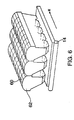
- reflecting means 18 further comprises a lenticular array of cylindrical microlenses 60 as shown in Fig. 6.
- the lenticular microlens curvature may have a shape other than cylindrical, such as, and for example only, an elliptical or a parabolic cross section.
- the microlenses 60 are disposed in close proximity to the microprisms 28.
- the microlenses 60 preferably have a index of refraction equal to the index of refraction of the microprisms 28.
- microlenses 60 could be fabricated in a separate process from the microprisms 28 and any transparent material may be used, as for example, those materials previously discussed.
- the index of refraction of the microlenses 60 be equal or substantially equal to the index of refraction of the microprisms 28.
- the center-to-center distance between microlenses directly correlates to the repeat distances 40 of the microprisms 28. That is, for every microprism 28 there exists a corresponding microlens 60 that aligns with the output surface 32 of each microprism 28.
- a spacer 62 separates the microlenses 60 and the microprisms 28.
- the thickness of spacer 62 is optimized to cause light from microprisms 28 to be collimated by microlenses 60.
- spacer 62 is molded in the same process that was used to mold microprisms 28 and microlenses 60 and therefore is the same material as the microprisms 28 and microlenses 60.
- spacer 62 may be fabricated separately from any transparent material.
- Preferred materials include transparent polymers, glass and fused silica.
- spacer 62 has an index of refraction equal to or substantially equal to the index of refraction of the microprisms 28 and the microlenses 60. Desired characteristics of these materials include mechanical and optical stability at typical operation temperatures of the device. Most preferred materials are glass, acrylic, polycarbonate and polyester.
- Arrays of microprisms 28 separately or in combination with microlenses 60 can be manufactured by any number of well known techniques such as molding, including injection and compression molding, casting, including hot roller pressing casting, photopolymerization within a mold and photopolymerization processes which do not employ a mold.
- One advantage of the invention over the prior art is the lenticular arrangement which facilitates the fabrication process by facilitating the free flow of resin within a mold.
- a preferred manufacturing technique would be one that allows the reflecting means 18 which comprises an array of microprisms 28, an array of microlenses 60 and a spacer 62 to be manufactured as a single integrated unit.
- An advantage of this technique would be the elimination of alignment errors between the array of microprisms and microlenses if the arrays were manufactured separately and then attached in the relationship described above.
- Preferably reflecting means 18 is manufactured by injection or compression molding.
- a polystyrene part was injection molded having lenticular prisms in combination with cylindrical lenses as shown in Fig. 6.
- the lenticular prisms were 0.3175mm (0.0125 inches) wide at the base of the prism and 0.5mm (0.020 inches) wide at the top of the prism.
- the prisms had a height of 0.48mm (0.019 inches).
- the cylindrical lenses were separated from the tops of the prisms by a polystyrene spacer layer 0.635mm (0.025 inches) thick. There was one cylindrical lens for each lenticular prism.
- the cylindrical lenses had a radius of curvature of 0.61mm (0.024 inches) and were aligned with the tops of the prisms.
- the lenticular prisms had "V-shaped" grooves or voids positioned every 0.41mm (0.016 inches) along the long direction of the prisms.
- the depth of the grooves was 0.25mm (0.0097 inches).
- the polystyrene part was attached to a clear acrylic waveguide using a silicone pressure-sensitive adhesive layer 0.24mm (0.001 inches thick).
- Light from two fluorescent lamps was coupled into two opposing ends of the acrylic waveguide. The general direction of the light was parallel to the direction of the lenticular prisms and lenses of the attached molded part. Light in the waveguide was able to pass through the silicone layer and enter the molded part in the regions where the molded part touched the pressure-sensitive adhesive.
- the surface area on the waveguide occupied by the voids did not allow light to pass from the waveguide.
- the walls of the void redirected light within the lenticular prisms.
- the light emerged from the molded part highly collimated and in a direction approximately perpendicular to the plane of the waveguide.
- the light had collimation angles (the full width of the peak at the half maximum points) of ⁇ 14° in one direction and ⁇ 13.7° in the perpendicular direction.
- Cross-sectional views of the light distribution in two perpendicular directions are shown in Figure 7.
Landscapes
- Physics & Mathematics (AREA)
- General Physics & Mathematics (AREA)
- Optics & Photonics (AREA)
- Engineering & Computer Science (AREA)
- General Engineering & Computer Science (AREA)
- Light Guides In General And Applications Therefor (AREA)
- Planar Illumination Modules (AREA)
- Optical Elements Other Than Lenses (AREA)
Applications Claiming Priority (3)
| Application Number | Priority Date | Filing Date | Title |
|---|---|---|---|
| US33772 | 1993-03-18 | ||
| US09/033,772 US5949933A (en) | 1998-03-03 | 1998-03-03 | Lenticular illumination system |
| PCT/US1999/004567 WO1999045317A1 (en) | 1998-03-03 | 1999-03-03 | A lenticular illumination system |
Publications (2)
| Publication Number | Publication Date |
|---|---|
| EP1060344A1 EP1060344A1 (en) | 2000-12-20 |
| EP1060344B1 true EP1060344B1 (en) | 2004-05-12 |
Family
ID=21872359
Family Applications (1)
| Application Number | Title | Priority Date | Filing Date |
|---|---|---|---|
| EP99911043A Expired - Lifetime EP1060344B1 (en) | 1998-03-03 | 1999-03-03 | A lenticular illumination system |
Country Status (8)
| Country | Link |
|---|---|
| US (1) | US5949933A (https=) |
| EP (1) | EP1060344B1 (https=) |
| JP (1) | JP2002506268A (https=) |
| KR (1) | KR100560193B1 (https=) |
| AU (1) | AU2977999A (https=) |
| CA (1) | CA2322326C (https=) |
| DE (1) | DE69917232T2 (https=) |
| WO (1) | WO1999045317A1 (https=) |
Cited By (13)
| Publication number | Priority date | Publication date | Assignee | Title |
|---|---|---|---|---|
| WO2022026536A1 (en) | 2020-07-29 | 2022-02-03 | Reald Spark, Llc | Backlight for switchable directional display |
| US12066717B2 (en) | 2017-09-15 | 2024-08-20 | Reald Spark, Llc | Optical stack for switchable directional display |
| US12117621B2 (en) | 2019-12-10 | 2024-10-15 | RealD Spark | Control of reflections of a display device |
| US12140847B2 (en) | 2018-10-03 | 2024-11-12 | ReaID Spark, LLC | Display apparatus using application software context for privacy control |
| US12169339B2 (en) | 2018-01-25 | 2024-12-17 | Reald Spark, Llc | Touch screen for privacy display |
| US12174504B2 (en) | 2018-07-18 | 2024-12-24 | Reald Spark, Llc | Optical stack for switchable directional display |
| US12228835B2 (en) | 2019-11-13 | 2025-02-18 | ReaID Spark, LLC | Display device with uniform off-axis luminance reduction |
| US12253748B2 (en) | 2023-04-25 | 2025-03-18 | Reald Spark, Llc | Switchable privacy display |
| US12259608B2 (en) | 2022-02-09 | 2025-03-25 | Reald Spark, Llc | Observer-tracked privacy display |
| US12366701B2 (en) | 2017-05-08 | 2025-07-22 | Reald Spark, Llc | Optical stack for imaging directional backlights |
| US12392949B2 (en) | 2016-05-19 | 2025-08-19 | Reald Spark, Llc | Wide angle imaging directional backlights |
| US12393066B2 (en) | 2023-08-03 | 2025-08-19 | Reald Spark, Llc | Privacy displays |
| US12587618B2 (en) | 2022-02-09 | 2026-03-24 | Reald Spark, Llc | Display device with uniform off-axis luminance reduction |
Families Citing this family (56)
| Publication number | Priority date | Publication date | Assignee | Title |
|---|---|---|---|---|
| CA2392947A1 (en) | 1999-11-30 | 2001-06-21 | Reflexite Corporation | Luminaire system |
| RU2183338C2 (ru) * | 2000-01-17 | 2002-06-10 | Дальневосточный государственный технический университет | Оптический элемент |
| US20040012832A1 (en) * | 2000-10-11 | 2004-01-22 | Gallen Niall Anthony | Beam expansion |
| US6535674B2 (en) * | 2000-12-15 | 2003-03-18 | Scram Technologies, Inc. | High contrast front projection display panel and a method of making a high contrast front projection display panel |
| JP2004198536A (ja) * | 2002-12-16 | 2004-07-15 | Three M Innovative Properties Co | レンズアレイシート及び成形方法 |
| US7245435B2 (en) * | 2002-12-16 | 2007-07-17 | 3M Innovative Properties Company | Lens array sheet and molding method |
| KR100714457B1 (ko) * | 2005-06-20 | 2007-05-04 | 한국에너지기술연구원 | 빛의 산란을 유도하는 광추출기 |
| CN101300521B (zh) * | 2005-11-04 | 2010-04-14 | 夏普株式会社 | 液晶显示装置 |
| US7366393B2 (en) * | 2006-01-13 | 2008-04-29 | Optical Research Associates | Light enhancing structures with three or more arrays of elongate features |
| US7866871B2 (en) * | 2006-01-13 | 2011-01-11 | Avery Dennison Corporation | Light enhancing structures with a plurality of arrays of elongate features |
| US7545569B2 (en) | 2006-01-13 | 2009-06-09 | Avery Dennison Corporation | Optical apparatus with flipped compound prism structures |
| US7674028B2 (en) * | 2006-01-13 | 2010-03-09 | Avery Dennison Corporation | Light enhancing structures with multiple arrays of elongate features of varying characteristics |
| US20070086207A1 (en) * | 2006-01-13 | 2007-04-19 | Optical Research Associates | Display systems including light enhancing structures with arrays of elongate features |
| US7593615B2 (en) * | 2006-02-10 | 2009-09-22 | Rpc Photonics, Inc. | Optical devices for guiding illumination |
| JP3898217B1 (ja) * | 2006-05-30 | 2007-03-28 | 日立マクセル株式会社 | バックライトユニットおよび液晶表示装置 |
| WO2007143347A2 (en) * | 2006-06-02 | 2007-12-13 | 3M Innovative Properties Company | Fluorescent volume light source |
| US20070279914A1 (en) * | 2006-06-02 | 2007-12-06 | 3M Innovative Properties Company | Fluorescent volume light source with reflector |
| US20070279915A1 (en) * | 2006-06-02 | 2007-12-06 | 3M Innovative Properties Company | Fluorescent Volume Light Source With Air Gap Cooling |
| US20070280622A1 (en) * | 2006-06-02 | 2007-12-06 | 3M Innovative Properties Company | Fluorescent light source having light recycling means |
| US7857457B2 (en) * | 2006-09-29 | 2010-12-28 | 3M Innovative Properties Company | Fluorescent volume light source having multiple fluorescent species |
| KR100811032B1 (ko) * | 2006-10-17 | 2008-03-06 | 삼성전기주식회사 | 모노리틱 조명장치 |
| EP2124095A4 (en) * | 2006-12-11 | 2010-09-01 | Sharp Kk | LIQUID CRYSTAL DISPLAY DEVICE |
| GB0704803D0 (en) * | 2007-03-13 | 2007-04-18 | Cambridge Flat Projection | Structured colour illumination of lcd's |
| US20080285304A1 (en) * | 2007-05-18 | 2008-11-20 | Rankin Jr Charles M | Light extraction film system |
| US20080285125A1 (en) * | 2007-05-18 | 2008-11-20 | Fujifilm Manufacturing U.S.A. Inc. | Optical panel for front projection under ambient lighting conditions |
| US7496263B2 (en) * | 2007-06-07 | 2009-02-24 | Fujifilm Manfacturing U.S.A. Inc. | Thermosetting optical waveguide coating |
| US20080305255A1 (en) * | 2007-06-07 | 2008-12-11 | Fujifilm Manufacturing U.S.A. Inc. | Optical waveguide coating |
| US9151884B2 (en) * | 2008-02-01 | 2015-10-06 | 3M Innovative Properties Company | Fluorescent volume light source with active chromphore |
| FR2948174A1 (fr) * | 2009-07-17 | 2011-01-21 | Franck Andre Marie Guigan | Paroi lumineuse |
| US20140140091A1 (en) | 2012-11-20 | 2014-05-22 | Sergiy Victorovich Vasylyev | Waveguide illumination system |
| US10436969B2 (en) | 2013-01-30 | 2019-10-08 | Ideal Industries Lighting Llc | Optical waveguide and luminaire incorporating same |
| US9291320B2 (en) | 2013-01-30 | 2016-03-22 | Cree, Inc. | Consolidated troffer |
| US9625638B2 (en) | 2013-03-15 | 2017-04-18 | Cree, Inc. | Optical waveguide body |
| US9442243B2 (en) | 2013-01-30 | 2016-09-13 | Cree, Inc. | Waveguide bodies including redirection features and methods of producing same |
| US9366396B2 (en) | 2013-01-30 | 2016-06-14 | Cree, Inc. | Optical waveguide and lamp including same |
| US9690029B2 (en) | 2013-01-30 | 2017-06-27 | Cree, Inc. | Optical waveguides and luminaires incorporating same |
| US9869432B2 (en) | 2013-01-30 | 2018-01-16 | Cree, Inc. | Luminaires using waveguide bodies and optical elements |
| US10379278B2 (en) * | 2013-03-15 | 2019-08-13 | Ideal Industries Lighting Llc | Outdoor and/or enclosed structure LED luminaire outdoor and/or enclosed structure LED luminaire having outward illumination |
| US10502899B2 (en) | 2013-03-15 | 2019-12-10 | Ideal Industries Lighting Llc | Outdoor and/or enclosed structure LED luminaire |
| US9798072B2 (en) | 2013-03-15 | 2017-10-24 | Cree, Inc. | Optical element and method of forming an optical element |
| US10209429B2 (en) | 2013-03-15 | 2019-02-19 | Cree, Inc. | Luminaire with selectable luminous intensity pattern |
| US10400984B2 (en) | 2013-03-15 | 2019-09-03 | Cree, Inc. | LED light fixture and unitary optic member therefor |
| US10436970B2 (en) | 2013-03-15 | 2019-10-08 | Ideal Industries Lighting Llc | Shaped optical waveguide bodies |
| US9366799B2 (en) | 2013-03-15 | 2016-06-14 | Cree, Inc. | Optical waveguide bodies and luminaires utilizing same |
| US9920901B2 (en) | 2013-03-15 | 2018-03-20 | Cree, Inc. | LED lensing arrangement |
| US9645303B2 (en) | 2013-03-15 | 2017-05-09 | Cree, Inc. | Luminaires utilizing edge coupling |
| DE102013021053B4 (de) * | 2013-12-18 | 2018-03-01 | Erco Gmbh | Leuchte |
| US9651740B2 (en) | 2014-01-09 | 2017-05-16 | Cree, Inc. | Extraction film for optical waveguide and method of producing same |
| US12372219B2 (en) * | 2014-05-30 | 2025-07-29 | Cree Lighting Usa Llc | LED luminaire with a cavity, finned interior, and a curved outer wall extending from a surface on which the light source is mounted |
| WO2016003550A2 (en) | 2014-07-03 | 2016-01-07 | Cree, Inc. | Waveguide having unidirectional illuminance |
| CN104834048B (zh) * | 2015-05-14 | 2018-01-26 | 北京京东方茶谷电子有限公司 | 一种显示面板、多面显示结构和显示装置 |
| US11719882B2 (en) | 2016-05-06 | 2023-08-08 | Ideal Industries Lighting Llc | Waveguide-based light sources with dynamic beam shaping |
| US10416377B2 (en) | 2016-05-06 | 2019-09-17 | Cree, Inc. | Luminaire with controllable light emission |
| WO2018144720A1 (en) * | 2017-02-01 | 2018-08-09 | Corning Incorporated | Light guide assemblies comprising optical manipulation features |
| KR102561280B1 (ko) * | 2018-03-21 | 2023-08-01 | 삼성디스플레이 주식회사 | 백라이트 유닛 및 이를 포함한 표시 장치 |
| WO2021209492A1 (en) * | 2020-04-15 | 2021-10-21 | CommScope Connectivity Belgium BV | Device and method for sealing cables in telecommunications enclosures |
Family Cites Families (14)
| Publication number | Priority date | Publication date | Assignee | Title |
|---|---|---|---|---|
| JPS5699332A (en) * | 1980-01-10 | 1981-08-10 | Canon Inc | Information mark display device |
| US4498742A (en) * | 1981-09-10 | 1985-02-12 | Nippon Kogaku K.K. | Illumination optical arrangement |
| JP3236631B2 (ja) * | 1991-01-25 | 2001-12-10 | ソリッド ステイト オプト リミテッド | パネル照明器 |
| TW594115B (en) * | 1992-10-09 | 2004-06-21 | Asahi Glass Co Ltd | A liquid crystal display device and an illumination device for a direct viewing type display element |
| US5428468A (en) * | 1993-11-05 | 1995-06-27 | Alliedsignal Inc. | Illumination system employing an array of microprisms |
| US5555329A (en) | 1993-11-05 | 1996-09-10 | Alliesignal Inc. | Light directing optical structure |
| US5521725A (en) * | 1993-11-05 | 1996-05-28 | Alliedsignal Inc. | Illumination system employing an array of microprisms |
| US5396350A (en) | 1993-11-05 | 1995-03-07 | Alliedsignal Inc. | Backlighting apparatus employing an array of microprisms |
| JPH08221013A (ja) * | 1994-12-15 | 1996-08-30 | Sony Corp | 平面表示装置および平面表示装置用バックライト装置 |
| GB2296808A (en) * | 1994-12-29 | 1996-07-10 | Sharp Kk | Illumination system for display device |
| JP4168179B2 (ja) * | 1995-03-03 | 2008-10-22 | スリーエム カンパニー | 種々の高さの構造化面を有する光指向性フィルム及び該フィルムから作製された光指向性製品 |
| US5838403A (en) * | 1996-02-14 | 1998-11-17 | Physical Optics Corporation | Liquid crystal display system with internally reflecting waveguide for backlighting and non-Lambertian diffusing |
| US5914760A (en) * | 1996-06-21 | 1999-06-22 | Casio Computer Co., Ltd. | Surface light source device and liquid crystal display device using the same |
| JP3355935B2 (ja) * | 1996-06-21 | 2002-12-09 | カシオ計算機株式会社 | 光源装置 |
-
1998
- 1998-03-03 US US09/033,772 patent/US5949933A/en not_active Expired - Lifetime
-
1999
- 1999-03-03 EP EP99911043A patent/EP1060344B1/en not_active Expired - Lifetime
- 1999-03-03 AU AU29779/99A patent/AU2977999A/en not_active Abandoned
- 1999-03-03 WO PCT/US1999/004567 patent/WO1999045317A1/en not_active Ceased
- 1999-03-03 DE DE69917232T patent/DE69917232T2/de not_active Expired - Lifetime
- 1999-03-03 KR KR1020007009724A patent/KR100560193B1/ko not_active Expired - Fee Related
- 1999-03-03 JP JP2000534812A patent/JP2002506268A/ja active Pending
- 1999-03-03 CA CA002322326A patent/CA2322326C/en not_active Expired - Fee Related
Cited By (15)
| Publication number | Priority date | Publication date | Assignee | Title |
|---|---|---|---|---|
| US12392949B2 (en) | 2016-05-19 | 2025-08-19 | Reald Spark, Llc | Wide angle imaging directional backlights |
| US12366701B2 (en) | 2017-05-08 | 2025-07-22 | Reald Spark, Llc | Optical stack for imaging directional backlights |
| US12066717B2 (en) | 2017-09-15 | 2024-08-20 | Reald Spark, Llc | Optical stack for switchable directional display |
| US12169339B2 (en) | 2018-01-25 | 2024-12-17 | Reald Spark, Llc | Touch screen for privacy display |
| US12174504B2 (en) | 2018-07-18 | 2024-12-24 | Reald Spark, Llc | Optical stack for switchable directional display |
| US12140847B2 (en) | 2018-10-03 | 2024-11-12 | ReaID Spark, LLC | Display apparatus using application software context for privacy control |
| US12228835B2 (en) | 2019-11-13 | 2025-02-18 | ReaID Spark, LLC | Display device with uniform off-axis luminance reduction |
| US12117621B2 (en) | 2019-12-10 | 2024-10-15 | RealD Spark | Control of reflections of a display device |
| WO2022026536A1 (en) | 2020-07-29 | 2022-02-03 | Reald Spark, Llc | Backlight for switchable directional display |
| EP4189285A4 (en) * | 2020-07-29 | 2024-07-24 | RealD Spark, LLC | BACKLIGHT FOR SWITCHABLE DIRECTIONAL DISPLAY |
| US12259608B2 (en) | 2022-02-09 | 2025-03-25 | Reald Spark, Llc | Observer-tracked privacy display |
| US12587618B2 (en) | 2022-02-09 | 2026-03-24 | Reald Spark, Llc | Display device with uniform off-axis luminance reduction |
| US12253748B2 (en) | 2023-04-25 | 2025-03-18 | Reald Spark, Llc | Switchable privacy display |
| US12523899B2 (en) | 2023-04-25 | 2026-01-13 | Reald Spark, Llc | Switchable privacy display |
| US12393066B2 (en) | 2023-08-03 | 2025-08-19 | Reald Spark, Llc | Privacy displays |
Also Published As
| Publication number | Publication date |
|---|---|
| CA2322326A1 (en) | 1999-09-10 |
| WO1999045317A1 (en) | 1999-09-10 |
| AU2977999A (en) | 1999-09-20 |
| KR100560193B1 (ko) | 2006-03-13 |
| US5949933A (en) | 1999-09-07 |
| EP1060344A1 (en) | 2000-12-20 |
| JP2002506268A (ja) | 2002-02-26 |
| CA2322326C (en) | 2004-09-14 |
| DE69917232T2 (de) | 2005-05-04 |
| DE69917232D1 (de) | 2004-06-17 |
| KR20010041544A (ko) | 2001-05-25 |
Similar Documents
| Publication | Publication Date | Title |
|---|---|---|
| EP1060344B1 (en) | A lenticular illumination system | |
| EP0801717B1 (en) | Illumination system employing an array of microprisms | |
| EP0749550B1 (en) | Illumination system employing an array of microprisms | |
| US6129439A (en) | Illumination system employing an array of multi-faceted microprisms | |
| JP2002506268A5 (https=) | ||
| EP1662279B1 (en) | Prism sheet and backlight unit employing the same | |
| US20060250707A1 (en) | Optical film having a surface with rounded pyramidal structures | |
| CN1124434C (zh) | 有一组线性棱镜的照明系统 | |
| US20060103777A1 (en) | Optical film having a structured surface with rectangular based prisms | |
| KR20090104077A (ko) | 조명 애플리케이션들을 위한 인커플링 구조물 | |
| EP0787271B1 (en) | Illumination system employing an array of multi-faceted microprisms | |
| CN101095077A (zh) | 具有带凹入的棱锥形结构的结构化表面的光学薄膜 | |
| JPH08248421A (ja) | 導光部材 | |
| JP2004319399A (ja) | 導光ブロックおよび平面照明装置 |
Legal Events
| Date | Code | Title | Description |
|---|---|---|---|
| PUAI | Public reference made under article 153(3) epc to a published international application that has entered the european phase |
Free format text: ORIGINAL CODE: 0009012 |
|
| 17P | Request for examination filed |
Effective date: 20000920 |
|
| AK | Designated contracting states |
Kind code of ref document: A1 Designated state(s): DE FR GB NL |
|
| 17Q | First examination report despatched |
Effective date: 20020705 |
|
| GRAP | Despatch of communication of intention to grant a patent |
Free format text: ORIGINAL CODE: EPIDOSNIGR1 |
|
| GRAS | Grant fee paid |
Free format text: ORIGINAL CODE: EPIDOSNIGR3 |
|
| GRAA | (expected) grant |
Free format text: ORIGINAL CODE: 0009210 |
|
| AK | Designated contracting states |
Kind code of ref document: B1 Designated state(s): DE FR GB NL |
|
| REG | Reference to a national code |
Ref country code: GB Ref legal event code: FG4D |
|
| REF | Corresponds to: |
Ref document number: 69917232 Country of ref document: DE Date of ref document: 20040617 Kind code of ref document: P |
|
| ET | Fr: translation filed | ||
| PLBE | No opposition filed within time limit |
Free format text: ORIGINAL CODE: 0009261 |
|
| STAA | Information on the status of an ep patent application or granted ep patent |
Free format text: STATUS: NO OPPOSITION FILED WITHIN TIME LIMIT |
|
| 26N | No opposition filed |
Effective date: 20050215 |
|
| REG | Reference to a national code |
Ref country code: GB Ref legal event code: 732E Free format text: REGISTERED BETWEEN 20120920 AND 20120926 |
|
| REG | Reference to a national code |
Ref country code: FR Ref legal event code: TP Owner name: SITECO BELEUCHTUNGSTECHNIK GMBH, DE Effective date: 20130502 Ref country code: FR Ref legal event code: CD Owner name: SITECO BELEUCHTUNGSTECHNIK GMBH, DE Effective date: 20130502 |
|
| REG | Reference to a national code |
Ref country code: NL Ref legal event code: SD Owner name: SITECO BELEUCHTUNGSTECHNIK GMBH, DE Effective date: 20131128 Ref country code: NL Ref legal event code: TD Effective date: 20131128 Ref country code: NL Ref legal event code: SD Effective date: 20131128 |
|
| REG | Reference to a national code |
Ref country code: FR Ref legal event code: PLFP Year of fee payment: 18 |
|
| REG | Reference to a national code |
Ref country code: DE Ref legal event code: R081 Ref document number: 69917232 Country of ref document: DE Owner name: SITECO BELEUCHTUNGSTECHNIK GMBH, DE Free format text: FORMER OWNER: ALLIEDSIGNAL INC., MORRISTOWN, N.J., US |
|
| REG | Reference to a national code |
Ref country code: FR Ref legal event code: PLFP Year of fee payment: 19 |
|
| PGFP | Annual fee paid to national office [announced via postgrant information from national office to epo] |
Ref country code: FR Payment date: 20170322 Year of fee payment: 19 Ref country code: NL Payment date: 20170321 Year of fee payment: 19 Ref country code: DE Payment date: 20170322 Year of fee payment: 19 |
|
| PGFP | Annual fee paid to national office [announced via postgrant information from national office to epo] |
Ref country code: GB Payment date: 20170322 Year of fee payment: 19 |
|
| REG | Reference to a national code |
Ref country code: DE Ref legal event code: R119 Ref document number: 69917232 Country of ref document: DE |
|
| REG | Reference to a national code |
Ref country code: NL Ref legal event code: MM Effective date: 20180401 |
|
| GBPC | Gb: european patent ceased through non-payment of renewal fee |
Effective date: 20180303 |
|
| PG25 | Lapsed in a contracting state [announced via postgrant information from national office to epo] |
Ref country code: NL Free format text: LAPSE BECAUSE OF NON-PAYMENT OF DUE FEES Effective date: 20180401 |
|
| PG25 | Lapsed in a contracting state [announced via postgrant information from national office to epo] |
Ref country code: DE Free format text: LAPSE BECAUSE OF NON-PAYMENT OF DUE FEES Effective date: 20181002 |
|
| PG25 | Lapsed in a contracting state [announced via postgrant information from national office to epo] |
Ref country code: GB Free format text: LAPSE BECAUSE OF NON-PAYMENT OF DUE FEES Effective date: 20180303 |
|
| PG25 | Lapsed in a contracting state [announced via postgrant information from national office to epo] |
Ref country code: FR Free format text: LAPSE BECAUSE OF NON-PAYMENT OF DUE FEES Effective date: 20180331 |