EP1054443A2 - Waferätzverfahren - Google Patents
Waferätzverfahren Download PDFInfo
- Publication number
- EP1054443A2 EP1054443A2 EP00105309A EP00105309A EP1054443A2 EP 1054443 A2 EP1054443 A2 EP 1054443A2 EP 00105309 A EP00105309 A EP 00105309A EP 00105309 A EP00105309 A EP 00105309A EP 1054443 A2 EP1054443 A2 EP 1054443A2
- Authority
- EP
- European Patent Office
- Prior art keywords
- gas
- wafer
- activated species
- silicon wafer
- mixed gas
- Prior art date
- Legal status (The legal status is an assumption and is not a legal conclusion. Google has not performed a legal analysis and makes no representation as to the accuracy of the status listed.)
- Withdrawn
Links
Images


Classifications
-
- H—ELECTRICITY
- H01—ELECTRIC ELEMENTS
- H01J—ELECTRIC DISCHARGE TUBES OR DISCHARGE LAMPS
- H01J37/00—Discharge tubes with provision for introducing objects or material to be exposed to the discharge, e.g. for the purpose of examination or processing thereof
- H01J37/32—Gas-filled discharge tubes
- H01J37/32009—Arrangements for generation of plasma specially adapted for examination or treatment of objects, e.g. plasma sources
- H01J37/32192—Microwave generated discharge
-
- H—ELECTRICITY
- H01—ELECTRIC ELEMENTS
- H01J—ELECTRIC DISCHARGE TUBES OR DISCHARGE LAMPS
- H01J37/00—Discharge tubes with provision for introducing objects or material to be exposed to the discharge, e.g. for the purpose of examination or processing thereof
- H01J37/32—Gas-filled discharge tubes
- H01J37/32009—Arrangements for generation of plasma specially adapted for examination or treatment of objects, e.g. plasma sources
- H01J37/32357—Generation remote from the workpiece, e.g. down-stream
-
- H—ELECTRICITY
- H01—ELECTRIC ELEMENTS
- H01J—ELECTRIC DISCHARGE TUBES OR DISCHARGE LAMPS
- H01J37/00—Discharge tubes with provision for introducing objects or material to be exposed to the discharge, e.g. for the purpose of examination or processing thereof
- H01J37/32—Gas-filled discharge tubes
- H01J37/32009—Arrangements for generation of plasma specially adapted for examination or treatment of objects, e.g. plasma sources
- H01J37/32366—Localised processing
-
- H10P50/242—
Definitions
- the present invention relates to a wafer etching method for locally etching relatively thick portions present on the surface of a wafer.
- TTV total thickness variation
- LTV local thickness variation
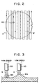
- FIG. 7 is a schematic view of a wafer etching method of the related art.
- reference numeral 100 represents a plasma generator.
- the plasma generator 100 causes plasma discharge of sulfur hexafluoride (SF 6 ) to generate an activated species gas G containing fluorine (F) ions and radicals.
- This activated species gas G is sprayed on to the surface of a silicon wafer W from a nozzle 101.
- the silicon wafer W is fixed on a stage 120.
- the stage 120 is made to move in the horizontal direction and the nozzle 101 made to scan the entire surface of the silicon wafer W, whereby portions Wa relatively thicker than the prescribed thickness on the surface of the silicon wafer W (hereinafter referred to as the "relatively thick portions") are led directly under the nozzle 101.
- the activated species gas G is sprayed on the protruding relatively thick portions Wa from the nozzle 101 and the relatively thick portions Wa are locally etched, whereby the surface of the silicon wafer W is flattened.
- white turbidity B occurs at the surface of the silicon wafer W along the line of scanning A of the nozzle 101 at the time of etching. Not only is the surface of the silicon wafer W contaminated, but also the white turbidity inhibits uniform etching and can cause the TTV and LTV to become worse than desired.
- the silicon wafer W is placed in a low atmospheric pressure environment of 1 Torr.
- a small discharge chamber 200 serving also as an electrode and filled with SF 6 gas is brought close to a relatively thick portion Wa.
- plasma discharge of the SF 6 gas is caused at a high frequency of 13.56 MHZ, whereby the relatively thick portion Wa is locally etched.
- the plasma in the discharge chamber 200 is close to the relatively thick portion Wa, at the same time as the activated species gas G etching the relatively thick portion Wa, the ions in the activated species gas G strike the relatively thick portion Wa. Therefore, it is believed, the white turbidity is eliminated by the impact of the various types of ions and no white turbidity remains on the surface of the silicon wafer Wa.
- the apparatus shown in FIG. 7 uses SF 6 gas, has a plasma discharge position far away from the silicon wafer W, and sprays only activated species gas G to the silicon wafer W. Therefore, so long as the silicon wafer W is etched by this apparatus, no disturbance occurs in the crystal structure of the silicon wafer W.
- the present inventors used this apparatus and added hydrogen (H 2 ) gas to the SF 6 gas to locally etch the silicon wafer W, then inspected the surface of the silicon wafer W visually, whereupon they failed to discern any white turbidity. This is believed to be because the occurrence of white turbidity was suppressed by the presence of the hydrogen fluoride (HF) produced by the reaction between the fluorine (F) radicals and H 2 . Further, with this method, since the ions in the activated species gas G do not strike the silicon wafer W, the crystal structure of the surface portion of the silicon wafer W is not disturbed. Further, it is believed that by heating the silicon wafer W to a predetermined temperature, it is possible to completely prevent the occurrence of white turbidity on the surface of the silicon wafer W.
- H 2 hydrogen
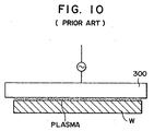
- This technique arranges the silicon wafer W inside a high atmospheric pressure environment of 1500 Torr.
- a drum shaped electrode 300 longer than the diameter of the silicon wafer W is brought close to the silicon wafer W and the SF 6 gas with the added H 2 gas is interposed in the slight clearance between the electrode 300 and the silicon wafer W.
- plasma discharge of the gas is caused by a high frequency of 150 MHZ, whereby the surface of the silicon wafer W is etched.
- the plasma discharge position is made close to the silicon wafer W, so similar problems arise as with the technique shown in FIG. 9.
- the atmospheric pressure is high, the temperature of the gas rises. As a result, the temperature of the wafer rises and problems such as warping of the wafer occurs. Further, it is not possible to suppress the occurrence of white turbidity.
- An object of the present invention is to provide a wafer etching method which adds hydrogen gas, ammonia gas or mixed gas containing one of these gases to sulfur hexafluoride gas and thereby suppresses the occurrence of white turbidity at the surface of the wafer at the time of etching and enables a high quality mirror polish to the wafer.
- a wafer etching method comprising: a plasma generation step for converting sulfur hexafluoride gas to plasma at a discharge position in a discharge tube to generate an activated species gas; and a spraying step for spraying the activated species gas on to a relatively thick portion, in a state where a nozzle portion of the discharge tube leading the activated species gas generated at the discharge position to the wafer side is made to face the relatively thick portion of the wafer, so as to locally etch the relatively thick portion, wherein hydrogen gas, ammonia gas or mixed gas containing one of these gases is added to the activated species gas in a predetermined ratio.
- the sulfur hexafluoride gas is converted to plasma at the discharge position in the discharge tube to generate an activated species gas.
- the activated species gas generated at the discharge position is led by the nozzle portion to the wafer side and the activated species gas from the nozzle portion facing a relatively thick portion of the wafer is sprayed to the relatively thick portion whereby the relatively thick portion is locally etched.
- the wafer is etched by the activated species gas comprised primarily of the sulfur hexafluoride gas, the etching rate is extremely high.
- the activated species gas is sprayed for etching from a nozzle portion away from the discharge position where the plasma is generated, the crystal structure of the wafer surface is not disturbed. Further, since hydrogen gas, ammonia gas or mixed gas containing one of these gases is added in a predetermined ratio to the activated species gas, the occurrence of white turbidity on the wafer surface can be suppressed.
- any method may be used to add the hydrogen gas, ammonia gas or mixed gas containing one of these gases to the activated species gas.
- a mixed gas comprising the sulfur hexafluoride gas in which hydrogen gas, ammonia gas or mixed gas containing one of these gases is mixed at a predetermined ratio is fed to the discharge position in the discharge tube to generate an activated species mixed gas containing the activated species gas and the activated species mixed gas is sprayed from the nozzle portion.
- the hydrogen gas, ammonia gas or mixed gas containing one of these gases is fed at a predetermined ratio from a gas feed pipe connected near the nozzle portion to the inside of the nozzle portion to generate an activated species mixed gas containing the activated species gas and the activated species mixed gas is sprayed from the nozzle portion.
- the activated species mixed gas is sprayed from the nozzle portion so as not to strike the wafer and to make the area around the wafer an atmosphere of the activated species mixed gas, then just sulfur hexafluoride gas is converted to plasma to generate an activated species gas for etching the wafer.
- any ratio of the hydrogen gas, ammonia gas or mixed gas containing one of these gases may be used, but as a good example, according to an aspect of the invention, the hydrogen gas, ammonia gas or mixed gas containing one of these gases is added in an amount of between 0.1 to 30 percent with respect to the mixed gas or the activated species mixed gas.
- hydrogen gas, ammonia gas or mixed gas containing one of these gases is filled around the activated species gas sprayed from the nozzle portion.
- the heating temperature of the wafer in the heating step is set to a temperature between 60°C to 170°C.
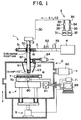
- FIG. 1 is a structural view of a wafer etching apparatus for realizing a wafer etching method according to a first embodiment of the present invention.
- This wafer etching apparatus is provided with a plasma generator 1 and a chamber 6 for accommodating a silicon wafer W.
- the plasma generator 1 has a discharge tube 2 formed by quartz or alumina, a gas feed system 3, a microwave oscillator 4, and a wave guide 5.
- the discharge tube 2 is a cylindrical body serving also as a nozzle portion 20 at its bottom end and having a feed pipe 30 of the gas feed system 3 connected to its top end.
- the gas feed system 3 is a system for feeding a gas into the discharge tube 2 and has a bomb 31 for the SF 6 gas and a bomb for the H 2 gas.
- the bombs 31 and 32 are connected through flow control devices 33 and 34 to a feed pipe 30.
- the microwave oscillator 4 is a magnetron and can generate a microwave M of a predetermined frequency.
- the wave guide 5 is for guiding the microwave M generated from the microwave oscillator 4 and is connected to the discharge tube 2 through a hole 50.
- this wave guide 5 At the inside of the left end of this wave guide 5 is attached a reflection plate (shot plunger) 51 for reflecting the microwave M and forming a standing wave. Further, in the middle of the wave guide 5 are attached a 3-stub tuner 52 for phase adjustment with the microwave M and an isolator 53 for bending the reflected microwave M heading toward the microwave oscillator 4 90° in direction (surface direction of FIG. 1).
- the position of insertion of the waveguide 5 over the microwave oscillator 4, that is, the discharge position is set far above the nozzle portion 20. Therefore, the plasma generated at the discharge position does not contribute itself to the etching of the silicon wafer W. Only the activated species gas G generated by the plasma discharge contributes to the etching of the silicon wafer W.
- the chamber 6 is a box-shaped member for accommodating the silicon wafer W and is evacuated by a vacuum pump 60.
- a hole 61 At the center of the top surface of the chamber 6 is formed a hole 61.
- the nozzle portion 20 of the discharge tube 2 is inserted into the chamber 6 through this hole 61.
- an O-ring 62 Between the hole 61 and the discharge tube 2 is fit an O-ring 62. The space between the hole 61 and the discharge tube 2 therefore can be held air-tight and the chamber 6 as a whole can be moved vertically with respect to the discharge tube 2.
- the vacuum pump 64 is driven to discharge the reaction product gas of the etching outside of the chamber 6.
- a chuck 7 is arranged inside the chamber 6.
- the silicon wafer W is held by this chuck 7.
- the chuck 7 is an electrostatic chuck and has a mechanism for holding the silicon wafer W by the force of static electricity. Further, inside the chuck 7, as shown by the broken line, is housed a heater 70. By turning the power supply 71 on, it is possible to heat the silicon wafer W to a predetermined temperature.
- the chuck 7 is supported by an X-Y drive mechanism 8. Further the chanter 6 as a whole is supported by a Z-drive mechanism 9.
- the chuck 7 is moved laterally in FIG. 1 by the X-drive motor 80 of the X-Y drive mechanism 8.
- the chuck 7 and the X-drive motor 80 are designed to be moved together in a direction perpendicular to the surface of the paper showing FIG. 1 by the Y-drive motor 81.
- the chanter 6 as a whole is designed to be moved vertically by a Z-drive motor 90 of the Z-drive mechanism 9.
- the drive operations of the X-drive motor 80 and Y-drive motor 81 of the X-Y drive mechanism 8 and the Z-drive motor 90 of the Z-drive mechanism 9 are controlled by a control computer 89 based on a predetermined program.
- the vacuum pump 60 is driven to make the inside of the chamber 6 a low atmospheric pressure state of 0.1 Torr to 5.0 Torr and the Z-drive mechanism 9 is driven to raise the chamber 6 as a whole and bring the silicon wafer W about 5 mm below the nozzle portion 20.
- valves 35 of the gas feed system 3 are opened and the SF 6 gas G1 in the bomb 31 and the H 2 gas G2 inside the bomb 32 are fed into the discharge tube 2 through the flow control devices 33 and 34 and the feed pipe 30.
- the opening degrees of the valves 35 are adjusted to maintain the pressures of the SF 6 gas G1 and the H 2 gas G2 at predetermined levels and the flow control devices 33 and 34 are used to adjust the flow rates of the SF 6 gas G1 and H 2 gas G2 to set the ratio of the H 2 gas G2 to the mixed gas of the SF 6 gas G1 and H 2 gas G2 fed into the discharge tube 2 to a value between 0.1 percent to 30 percent.
- the microwave M will cause plasma discharge of the mixed gas present at the discharge position and the activated species gas G and HF gas G3 will be produced (plasma generation step).
- the activated species mixed gas G' containing the activated species gas G and the HF gas is guided to the nozzle portion 20 and sprayed from the opening of the nozzle portion 20 to the silicon wafer W side.
- control computer 89 drives the X-Y drive mechanism 8 to move the chuck 7 holding the silicon wafer W zigzag in the X-Y direction.
- the nozzle portion 20 is made to scan relative to the silicon wafer W in a zigzag.
- the relative speed of the nozzle portion 20 with respect to the silicon wafer W is set to be substantially inversely proportional to the thickness of a relatively thick portion.
- the nozzle portion 20 moves at a high speed directly above a non-relatively thick portion Wb.
- the speed is lowered in accordance with the thickness of the relatively thick portion Wa.
- the etching time with respect to the relatively thick portion Wa becomes longer and the relatively thick portion Wa is shaved flat (spraying step).
- gaseous reaction product produced at the time of such etching is discharged outside of the chamber 6 from the duct 53 by the vacuum pump 64 shown in FIG. 1.
- an activated species mixed gas G' containing the activated species gas G containing F radicals and HF gas produced by a reaction between the F radicals and H 2 gas G2 is blown on to the silicon wafer W. Therefore, it is believed that the HF gas in the activated species mixed gas G' acts chemically and physically on the surface of the silicon wafer W and suppresses white turbidity on the surface of the silicon wafer W.
- the silicon wafer W is etched by the activated species gas G obtained by the plasma discharge of the SF 6 gas G1, the etching rate is fast.
- the discharge position of the plasma is set to a position far above the silicon wafer W (for example, a position 15 cm above the surface of the silicon wafer W), the plasma generated at the discharge position will not itself affect the etching of the silicon wafer W. That is, the plasma only will function as a source of production of the activated species gas G.
- the silicon wafer W is etched only by the activated species gas G. Therefore, there will be no disturbance of the crystal structure of the surface of the silicon wafer W by ions in the activated species gas G striking the silicon wafer W as in the related art shown in FIG. 9.
- the present inventors engaged in the following comparative experiments to verify the above advantageous effect.
- an 8-inch silicon wafer W was held by a chuck 7 in a chamber 6 held at 1 Torr, a valve 35 of the gas feed system 3 was opened, and the flow control device 33 was adjusted to feed 200 SCCM, that is, 200 liters per minute, of SF 6 gas from the bomb 31 to the discharge tube 2.
- a microwave M of an output of 300W was generated from the microwave oscillator 4 to cause plasma discharge of the SF 6 gas.
- the nozzle portion 20 was made to scan the surface in a zigzag at a pitch of 8 mm to etch the entire surface of the silicon wafer W by the activated species gas G sprayed from the nozzle portion 20. This being done, it was visually confirmed under natural light that the white turbidity B shown in FIG. 8 occurred along the scanning line A on the surface of the silicon wafer W after etching.
- the inventors conducted a second experiment, in which the valve 35 was opened and the flow control devices 33 and 34 were adjusted to output 200 SCCM of SF 6 gas G1 from the bomb 31 and output 10 SCCM of H 2 gas G2 from the bomb 32 and feed this mixed gas to the discharge tube 2.
- the other conditions were set the same as the conditions of the above first experiment. This being done, the occurrence of white turbidity could not be visually discerned under natural light at the surface of the silicon wafer W after etching. Further, it was possible to obtain a good quality mirror surface without disturbance of the crystal structure.
- a silicon wafer W having this extent of white turbidity is acceptable as a finished product, but to obtain a further higher quality mirror surface, it is necessary to give a mirror polish to the surface of the silicon wafer W by a chemical mechanical polishing (CMP) apparatus. Therefore, in this case, a mirror polishing step is needed, therefore the equipment costs more and the processing time of the work ends up becoming longer.
- CMP chemical mechanical polishing
- a heating step is provided which is able to substantially completely prevent the occurrence of white turbidity at the surface of the silicon wafer W without causing a rise in the cost of the equipment etc.
- the same procedure as with the wafer etching method of the first embodiment is performed and the power supply 71 is turned on to operate the heater 70 at the time of etching the silicon wafer W so as to heat the silicon wafer W to a temperature between 60°C to 170°C.
- the white turbidity on the surface of the silicon wafer W is reduced to an extent where it cannot be visually discerned even under a condenser type lamp.
- the present inventors verified this advantageous effect by conducting an experiment in which a silicon wafer W was etched under conditions similar to those of the above second experiment and the heater 70 was used to heat the silicon wafer W to a temperature of 80°C.
- the wafer etching method of this embodiment it is possible to perform processing the same as the above mirror polishing by a simple piece of equipment and possible to reduce the cost of the equipment and shorten the processing time.
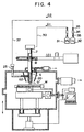
- FIG. 4 is a structural view of a wafer etching apparatus for realizing a wafer etching method according to a third embodiment of the present invention.
- This wafer etching apparatus is structured with an L-shaped hydrogen gas feed pipe 25 connected to the nozzle portion 20, a feed pipe 37 connected to the hydrogen gas feed pipe 25, and a bomb 32 connected to this feed pipe 37 through a valve 35 and a flow control device 34.
- the H 2 gas G2 discharged from the hydrogen gas feed pipe 25 is added to the activated species gas G produced by the plasma discharge of the SF 6 gas G1 and flowing to the nozzle portion 20 side.
- the activated species mixed gas G' produced by the addition of the H 2 gas G2 is sprayed from the opening of the nozzle portion 20 to the surface of the silicon wafer W.
- an activated species mixed gas G' containing HF gas obtained by adding H 2 gas G2 to the SF 6 gas G1 (or activated species gas G) is sprayed from the nozzle portion 20 to the inside of the chamber 6 to make the inside of the chamber 6 an HF gas atmosphere of a predetermined concentration. Due to this, an environment capable of preventing the occurrence of white turbidity on the surface of the silicon wafer W is created around the silicon wafer W.
- the silicon wafer W is conveyed into the chamber 6 and held by the chuck 7.
- the SF 6 gas G1 of the bomb 31 is fed to the discharge tube 2 and only the activated species gas G produced by the plasma discharge etches the silicon wafer W.
- the etching portion of the silicon wafer W is directly etched by the activated species gas G and the etching rate is improved.
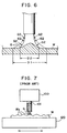
- FIG. 5 is a structural view of a wafer etching apparatus for realizing the wafer etching method according to a fifth embodiment of the present invention
- FIG. 6 is a schematic view for explaining the mode of operation of this embodiment.
- This wafer etching apparatus is structured with a straight hydrogen gas feed pipe 26, connected through the feed pipe 37 to the bomb 32, attached to the chamber 6 and opening inside the chamber 6.
- the SF 6 gas G1 is fed from the bomb 31 to the discharge tube 2 and the activated species gas G produced by the plasma discharge is sprayed from the nozzle portion 20.
- H 2 gas G2 is fed from the bomb 32 to the hydrogen gas feed pipe 26 and H 2 gas G2 is discharged from the hydrogen gas feed pipe 26 to the chamber 6 to fill the chamber 6 with H 2 gas G2.
- the dispersion of the activated species gas G is suppressed by the pressure of the H 2 gas G2 and, as shown by the solid line in FIG. 6, the etching diameter D2 becomes smaller.
- the wafer etching method of this embodiment differs from the first embodiment in the point that ammonia (NH 3 ) gas is used to etch wafer in stead of H 2 gas used in the first embodiment.
- ammonia (NH 3 ) gas is used to etch wafer in stead of H 2 gas used in the first embodiment.
- NH 3 gas is filled previously in the bomb 32 shown in Fig. 1. Then, at the time of feeding operation of the mixed gas, the ratio of NH 3 gas to the mixed gas of the SF 6 gas G1 and NH 3 gas fed into the discharge tube 2 is set to the value between 0.1 percent to 30 percent.
- the microwave oscillator 4 is driven to perform the plasma generation step.
- the activated species mixed gas G' comprising the activated species gas G and the HF gas is sprayed from the opening of the nozzle portion 20 to the silicon wafer W side. Thereafter, by performing the spraying step same as in the first embodiment, the silicon wafer W can be flattened.
- an activated species mixed gas G' containing the activated species gas G containing F radicals and HF gas produced by a reaction between the F radicals and NH 3 gas is blown on to the silicon wafer W, as is the case with the first embodiment. Therefore, it is believed that the HF gas in the activated species mixed gas G' acts chemically and physically on the surface of the silicon wafer W and suppresses white turbidity on the surface of the silicon wafer W.
- the bonding force of N-H in NH 3 gas is weaker than that of H-H in H 2 gas, H ions can easily be separated from N ions. Therefore, HF gas can be generated rapidly, so that the suppress effect on the generation of white turbidity is raised compared with the case using H 2 gas.
- NH 3 gas can easily be handled compared with H 2 gas which has high reactivity with oxygen in an air.
- H 2 gas is colorless and odorless, it is difficult to detect H 2 gas when H 2 gas is leaked from the bomb 32 and others.
- NH 3 gas has its odor, NH 3 gas can be detected immediately when NH 3 gas is leaked from the bomb 32 and others.
- a plasma generator 1 generating a microwave to generate plasma
- any means capable of generating activated species gas may be used.
- a heater 70 as a means for realizing the heating step, but the invention is not limited to this.
- an infrared lamp etc. as the means for executing the heating step.
- the silicon wafer W is heated to the temperature between 60°C and 170°C by operating the heater 70 shown in Fig. 1. Due to this, it is possible to suppress the white turbidity on the surface of the silicon wafer W to an extent where it cannot be visually discerned even under a condenser type lamp.
- an activated species mixed gas G' including HF gas obtaining by adding NH 3 gas to the SF 6 gas G1 (or activated species gas G) is sprayed from the nozzle portion 20 to the inside of the chamber 6 to make the inside of the chamber 6 an HF gas atmosphere of a predetermined concentration. Thereafter, only the activated species gas G produced by plasma discharge etches the silicon wafer W, so that it is possible to improve the etching rate.
- NH 3 gas is discharged from the gas feed pipe 26 into the chamber 6 and the chamber 26 is filled with NH 3 gas. Due to this, diffusion of the activated species gas G is suppressed by the pressure of NH 3 gas thereby enabling the etching diameter small.
- the wafer is etched by an activated species gas comprised mainly of sulfur hexafluoride, so it is possible to increase the etching rate of the wafer. Further, since the activated species gas is sprayed for etching from a nozzle portion far from the discharge position where the plasma is generated, there is no disturbance in the crystal structure of the wafer surface and a good quality wafer can be provided. Further, since the addition of hydrogen gas, ammonia gas or mixed gas containing one of these gases enables the occurrence of white turbidity of the wafer surface to be suppressed, it is possible to provide a high quality wafer.
- an activated species gas comprised mainly of sulfur hexafluoride
- the wafer etching method according to the aspect of the invention, only the activated species gas produced by converting only sulfur hexafluoride to plasma is sprayed at the time of etching the wafer, so the etching by the activated species is not obstructed much at all by the hydrogen gas, ammonia gas or mixed gas containing one of these gases. As a result, it is possible to make the etching rate a desired level and possible to improve the efficiency of the work.
- the wafer etching method not only is it possible to prevent the occurrence of white turbidity at the wafer surface, but also it is possible to control the etching diameter by the activated species gas to a desired size by the hydrogen gas, ammonia gas or mixed gas containing one of these gases, so high precision local etching becomes possible.
- the wafer etching method it is possible to substantially completely suppress the occurrence of white turbidity at the surface of the wafer to an extent where the white turbidity cannot be visually discerned even under a condenser type lamp, so a further higher quality wafer can be provided.
Landscapes
- Physics & Mathematics (AREA)
- Engineering & Computer Science (AREA)
- Plasma & Fusion (AREA)
- Chemical & Material Sciences (AREA)
- Analytical Chemistry (AREA)
- Drying Of Semiconductors (AREA)
- ing And Chemical Polishing (AREA)
Applications Claiming Priority (2)
| Application Number | Priority Date | Filing Date | Title |
|---|---|---|---|
| JP13203299A JP4424701B2 (ja) | 1998-06-09 | 1999-05-12 | ウエハエッチング方法 |
| JP13203299 | 1999-05-12 |
Publications (2)
| Publication Number | Publication Date |
|---|---|
| EP1054443A2 true EP1054443A2 (de) | 2000-11-22 |
| EP1054443A3 EP1054443A3 (de) | 2001-08-29 |
Family
ID=15071913
Family Applications (1)
| Application Number | Title | Priority Date | Filing Date |
|---|---|---|---|
| EP00105309A Withdrawn EP1054443A3 (de) | 1999-05-12 | 2000-03-15 | Waferätzverfahren |
Country Status (2)
| Country | Link |
|---|---|
| EP (1) | EP1054443A3 (de) |
| KR (1) | KR20000076861A (de) |
Cited By (1)
| Publication number | Priority date | Publication date | Assignee | Title |
|---|---|---|---|---|
| DE102015119325A1 (de) | 2015-11-10 | 2017-05-11 | Leibniz-Institut für Oberflächenmodifizierung e.V. | Verfahren zur Glättung von Oberflächen eines Werkstücks |
Families Citing this family (1)
| Publication number | Priority date | Publication date | Assignee | Title |
|---|---|---|---|---|
| JP2002343798A (ja) * | 2001-05-18 | 2002-11-29 | Mitsubishi Electric Corp | 配線層のドライエッチング方法、半導体装置の製造方法および該方法によって得られた半導体装置 |
Family Cites Families (8)
| Publication number | Priority date | Publication date | Assignee | Title |
|---|---|---|---|---|
| US4052251A (en) * | 1976-03-02 | 1977-10-04 | Rca Corporation | Method of etching sapphire utilizing sulfur hexafluoride |
| JPS58204537A (ja) * | 1982-05-24 | 1983-11-29 | Hitachi Ltd | プラズマエツチング方法 |
| JPS6432627A (en) * | 1987-07-29 | 1989-02-02 | Hitachi Ltd | Low-temperature dry etching method |
| JP3612158B2 (ja) * | 1996-11-18 | 2005-01-19 | スピードファム株式会社 | プラズマエッチング方法及びその装置 |
| JP3917703B2 (ja) * | 1997-02-18 | 2007-05-23 | スピードファム株式会社 | プラズマエッチング方法及びその装置 |
| JP2000036488A (ja) * | 1998-07-21 | 2000-02-02 | Speedfam-Ipec Co Ltd | ウエハ平坦化方法及びそのシステム |
| JP4212707B2 (ja) * | 1998-11-26 | 2009-01-21 | スピードファム株式会社 | ウエハ平坦化システム及びウエハ平坦化方法 |
| JP2000256094A (ja) * | 1999-03-08 | 2000-09-19 | Speedfam-Ipec Co Ltd | シリコンエピタキシャル成長ウェーハ製造方法およびその装置 |
-
2000
- 2000-03-15 EP EP00105309A patent/EP1054443A3/de not_active Withdrawn
- 2000-03-15 KR KR1020000013032A patent/KR20000076861A/ko not_active Ceased
Cited By (1)
| Publication number | Priority date | Publication date | Assignee | Title |
|---|---|---|---|---|
| DE102015119325A1 (de) | 2015-11-10 | 2017-05-11 | Leibniz-Institut für Oberflächenmodifizierung e.V. | Verfahren zur Glättung von Oberflächen eines Werkstücks |
Also Published As
| Publication number | Publication date |
|---|---|
| KR20000076861A (ko) | 2000-12-26 |
| EP1054443A3 (de) | 2001-08-29 |
Similar Documents
| Publication | Publication Date | Title |
|---|---|---|
| US4529475A (en) | Dry etching apparatus and method using reactive gases | |
| US6793736B2 (en) | Method of providing high flux of point of use activated reactive species for semiconductor processing | |
| KR102402866B1 (ko) | 고 종횡비의 구조체들의 콘택 세정 | |
| EP0168768B1 (de) | Trockenätzvorrichtung und Trockenätzprozess | |
| US6280645B1 (en) | Wafer flattening process and system | |
| US4687544A (en) | Method and apparatus for dry processing of substrates | |
| US6069092A (en) | Dry etching method and semiconductor device fabrication method | |
| CN107293470B (zh) | 用于在晶片上对层进行蚀刻的装置和方法 | |
| US20030170389A1 (en) | Atomic layer deposition with point of use generated reactive gas species | |
| US20090165953A1 (en) | Plasma Reactor | |
| JPH07278821A (ja) | プロセス・モジュールにおいてプラズマを点火する装置並びに方法 | |
| KR20090014151A (ko) | 상압 플라즈마 생성방법, 플라즈마 처리방법과 이를 이용한부품 실장방법, 및 이들 방법을 이용한 장치 | |
| TW202201536A (zh) | 利用氯之高深寬比介電質蝕刻 | |
| US20010032705A1 (en) | Local etching apparatus and local etching method | |
| US6451217B1 (en) | Wafer etching method | |
| EP1054443A2 (de) | Waferätzverfahren | |
| US20020008082A1 (en) | Local etching apparatus and local etching method | |
| US6303511B2 (en) | Wafer flattening process | |
| US6302995B1 (en) | Local etching apparatus | |
| US7270724B2 (en) | Scanning plasma reactor | |
| KR20030024386A (ko) | 플라즈마 발생장치 및 이를 이용한 SiO₂박막 식각방법 | |
| US20040142571A1 (en) | Local dry etching method | |
| US20150132929A1 (en) | Method for injecting dopant into substrate to be processed, and plasma doping apparatus | |
| US20010019040A1 (en) | Discharge tube for a local etching apparatus and a local etching apparatus using the discharge tube | |
| JPH09213686A (ja) | プラズマエッチング装置 |
Legal Events
| Date | Code | Title | Description |
|---|---|---|---|
| PUAI | Public reference made under article 153(3) epc to a published international application that has entered the european phase |
Free format text: ORIGINAL CODE: 0009012 |
|
| AK | Designated contracting states |
Kind code of ref document: A2 Designated state(s): AT BE CH CY DE DK ES FI FR GB GR IE IT LI LU MC NL PT SE |
|
| AX | Request for extension of the european patent |
Free format text: AL;LT;LV;MK;RO;SI |
|
| RAP1 | Party data changed (applicant data changed or rights of an application transferred) |
Owner name: HORIIKE, YASUHIRO Owner name: SPEEDFAM CO.,LTD. |
|
| PUAL | Search report despatched |
Free format text: ORIGINAL CODE: 0009013 |
|
| AK | Designated contracting states |
Kind code of ref document: A3 Designated state(s): AT BE CH CY DE DK ES FI FR GB GR IE IT LI LU MC NL PT SE |
|
| AX | Request for extension of the european patent |
Free format text: AL;LT;LV;MK;RO;SI |
|
| 17P | Request for examination filed |
Effective date: 20010918 |
|
| 17Q | First examination report despatched |
Effective date: 20011108 |
|
| AKX | Designation fees paid |
Free format text: DE FR GB NL |
|
| STAA | Information on the status of an ep patent application or granted ep patent |
Free format text: STATUS: THE APPLICATION IS DEEMED TO BE WITHDRAWN |
|
| 18D | Application deemed to be withdrawn |
Effective date: 20060607 |