EP1052747A2 - Semiconductor laser, semiconductor optical amplifier, and production method thereof - Google Patents
Semiconductor laser, semiconductor optical amplifier, and production method thereof Download PDFInfo
- Publication number
- EP1052747A2 EP1052747A2 EP00109903A EP00109903A EP1052747A2 EP 1052747 A2 EP1052747 A2 EP 1052747A2 EP 00109903 A EP00109903 A EP 00109903A EP 00109903 A EP00109903 A EP 00109903A EP 1052747 A2 EP1052747 A2 EP 1052747A2
- Authority
- EP
- European Patent Office
- Prior art keywords
- waveguide
- mode
- semiconductor laser
- mode waveguide
- single mode
- Prior art date
- Legal status (The legal status is an assumption and is not a legal conclusion. Google has not performed a legal analysis and makes no representation as to the accuracy of the status listed.)
- Granted
Links
Images


Classifications
-
- H—ELECTRICITY
- H01—ELECTRIC ELEMENTS
- H01S—DEVICES USING THE PROCESS OF LIGHT AMPLIFICATION BY STIMULATED EMISSION OF RADIATION [LASER] TO AMPLIFY OR GENERATE LIGHT; DEVICES USING STIMULATED EMISSION OF ELECTROMAGNETIC RADIATION IN WAVE RANGES OTHER THAN OPTICAL
- H01S5/00—Semiconductor lasers
- H01S5/10—Construction or shape of the optical resonator, e.g. extended or external cavity, coupled cavities, bent-guide, varying width, thickness or composition of the active region
-
- H—ELECTRICITY
- H01—ELECTRIC ELEMENTS
- H01S—DEVICES USING THE PROCESS OF LIGHT AMPLIFICATION BY STIMULATED EMISSION OF RADIATION [LASER] TO AMPLIFY OR GENERATE LIGHT; DEVICES USING STIMULATED EMISSION OF ELECTROMAGNETIC RADIATION IN WAVE RANGES OTHER THAN OPTICAL
- H01S5/00—Semiconductor lasers
- H01S5/06—Arrangements for controlling the laser output parameters, e.g. by operating on the active medium
- H01S5/065—Mode locking; Mode suppression; Mode selection ; Self pulsating
- H01S5/0651—Mode control
- H01S5/0653—Mode suppression, e.g. specific multimode
- H01S5/0655—Single transverse or lateral mode emission
-
- H—ELECTRICITY
- H01—ELECTRIC ELEMENTS
- H01S—DEVICES USING THE PROCESS OF LIGHT AMPLIFICATION BY STIMULATED EMISSION OF RADIATION [LASER] TO AMPLIFY OR GENERATE LIGHT; DEVICES USING STIMULATED EMISSION OF ELECTROMAGNETIC RADIATION IN WAVE RANGES OTHER THAN OPTICAL
- H01S5/00—Semiconductor lasers
- H01S5/10—Construction or shape of the optical resonator, e.g. extended or external cavity, coupled cavities, bent-guide, varying width, thickness or composition of the active region
- H01S5/1053—Comprising an active region having a varying composition or cross-section in a specific direction
- H01S5/1064—Comprising an active region having a varying composition or cross-section in a specific direction varying width along the optical axis
-
- H—ELECTRICITY
- H01—ELECTRIC ELEMENTS
- H01S—DEVICES USING THE PROCESS OF LIGHT AMPLIFICATION BY STIMULATED EMISSION OF RADIATION [LASER] TO AMPLIFY OR GENERATE LIGHT; DEVICES USING STIMULATED EMISSION OF ELECTROMAGNETIC RADIATION IN WAVE RANGES OTHER THAN OPTICAL
- H01S5/00—Semiconductor lasers
- H01S5/10—Construction or shape of the optical resonator, e.g. extended or external cavity, coupled cavities, bent-guide, varying width, thickness or composition of the active region
- H01S5/16—Window-type lasers, i.e. with a region of non-absorbing material between the active region and the reflecting surface
- H01S5/164—Window-type lasers, i.e. with a region of non-absorbing material between the active region and the reflecting surface with window regions comprising semiconductor material with a wider bandgap than the active layer
-
- H—ELECTRICITY
- H01—ELECTRIC ELEMENTS
- H01S—DEVICES USING THE PROCESS OF LIGHT AMPLIFICATION BY STIMULATED EMISSION OF RADIATION [LASER] TO AMPLIFY OR GENERATE LIGHT; DEVICES USING STIMULATED EMISSION OF ELECTROMAGNETIC RADIATION IN WAVE RANGES OTHER THAN OPTICAL
- H01S5/00—Semiconductor lasers
- H01S5/20—Structure or shape of the semiconductor body to guide the optical wave ; Confining structures perpendicular to the optical axis, e.g. index or gain guiding, stripe geometry, broad area lasers, gain tailoring, transverse or lateral reflectors, special cladding structures, MQW barrier reflection layers
- H01S5/2036—Broad area lasers
-
- H—ELECTRICITY
- H01—ELECTRIC ELEMENTS
- H01S—DEVICES USING THE PROCESS OF LIGHT AMPLIFICATION BY STIMULATED EMISSION OF RADIATION [LASER] TO AMPLIFY OR GENERATE LIGHT; DEVICES USING STIMULATED EMISSION OF ELECTROMAGNETIC RADIATION IN WAVE RANGES OTHER THAN OPTICAL
- H01S5/00—Semiconductor lasers
- H01S5/20—Structure or shape of the semiconductor body to guide the optical wave ; Confining structures perpendicular to the optical axis, e.g. index or gain guiding, stripe geometry, broad area lasers, gain tailoring, transverse or lateral reflectors, special cladding structures, MQW barrier reflection layers
- H01S5/22—Structure or shape of the semiconductor body to guide the optical wave ; Confining structures perpendicular to the optical axis, e.g. index or gain guiding, stripe geometry, broad area lasers, gain tailoring, transverse or lateral reflectors, special cladding structures, MQW barrier reflection layers having a ridge or stripe structure
- H01S5/223—Buried stripe structure
- H01S5/2231—Buried stripe structure with inner confining structure only between the active layer and the upper electrode
-
- H—ELECTRICITY
- H01—ELECTRIC ELEMENTS
- H01S—DEVICES USING THE PROCESS OF LIGHT AMPLIFICATION BY STIMULATED EMISSION OF RADIATION [LASER] TO AMPLIFY OR GENERATE LIGHT; DEVICES USING STIMULATED EMISSION OF ELECTROMAGNETIC RADIATION IN WAVE RANGES OTHER THAN OPTICAL
- H01S5/00—Semiconductor lasers
- H01S5/40—Arrangement of two or more semiconductor lasers, not provided for in groups H01S5/02 - H01S5/30
- H01S5/4025—Array arrangements, e.g. constituted by discrete laser diodes or laser bar
- H01S5/4031—Edge-emitting structures
- H01S5/4068—Edge-emitting structures with lateral coupling by axially offset or by merging waveguides, e.g. Y-couplers
-
- H—ELECTRICITY
- H01—ELECTRIC ELEMENTS
- H01S—DEVICES USING THE PROCESS OF LIGHT AMPLIFICATION BY STIMULATED EMISSION OF RADIATION [LASER] TO AMPLIFY OR GENERATE LIGHT; DEVICES USING STIMULATED EMISSION OF ELECTROMAGNETIC RADIATION IN WAVE RANGES OTHER THAN OPTICAL
- H01S5/00—Semiconductor lasers
- H01S5/50—Amplifier structures not provided for in groups H01S5/02 - H01S5/30
Abstract
Description
- The present invention relates to a semiconductor laser, a semiconductor optical amplifier, and a production method thereof.
- Nowadays, the opto-electronic technology is implemented to various fields, e.g. information I/O system such as compact disc application, and optical telecommunication system using optical fibers. As devices supporting the Opto-electronic technology, various semiconductor lasers have been developed. For example, as semiconductor lasers for the compact disc, those of near infrared or visible light band have been developed, and as semiconductor laser for optical telecommunication system, those of long wavelength band have been developed.
- As a type of the semiconductor laser, there is a waveguide type semiconductor laser. In general, the waveguide type semiconductor laser when used for information transmission or as an optical fiber amplification excitation source, its waveguide is designed so as to satisfy a single mode condition or a quasi-mode condition.
- In general, when a laser beam is used in multi mode, there arises a problem to be affected by the multi mode dispersion. When a signal light is coupled to an optical waveguide such as an optical fiber or to a lens, there arises a difficulty for coupling a signal light effectively. These problems can be eliminated by designing the waveguide as has been mentioned above.
- In order to satisfy the aforementioned single mode, various semiconductor lasers have been developed. (For example, Japanese Patent Publication 63-293989 discloses such a semiconductor laser element.) However, the configuration designed to satisfy the single mode condition has restricted the laser characteristics.
- For example, a width and a thickness of an active layer in a semiconductor laser have been limited within a predetermined range according to the single mode condition. Especially, in order to improve a gain saturation level, it is advantageous to enlarge the waveguide width. However, this is limited to a certain value because of the aforementioned single mode condition. Thus, semiconductor laser output power has been limited technically.
- An example of eliminating such limitation by the single mode condition is disclosed in L. J. Mawst et al "Phase-locked laser diode array", Applied Physics Letters Vol. 60, No. 6, 1992, pp. 668-670. In this phase-locked laser diode array, 20 semiconductor lasers of single mode are arranged at a predetermined interval in a direction vertical to the light waveguide, so that the semiconductor lasers produde resonance, thus enabling to finally obtain a high single mode output.
- However, this phase-locked laser diode array has a complicated configuration, which results in a low production yield.
- Moreover, when producing the phase-locked laser diode array so as to satisfy the resonance condition, the tolerance is very small and it is difficult to produce identical arrays.
- Furthermore, in addition to the active layer gain saturation, COD (catastrophic optical damage) and spatial hole burning are known as phenomena constricting the semiconductor laser output. In general, in order to improve the COD level, it is preferable to enlarge the waveguide width so as to reduce the light density per unit area of the cleaved facet.
- However, the waveguide width is under restriction of the single mode condition as is mentioned above. Furthermore, in order to suppress the spatial hole burning, in general, it is preferable to reduce the waveguide width. Thus, in order to obtain a high output in the conventional semiconductor laser, it is necessary to perform designing, satisfying the single mode condition and considering the COD level and the spatial hole burning which are in a trade off relationship with the single mode condition. Accordingly, it has been tremendously difficult to obtain a high output of a semiconductor laser.
- As a method to improve the aforementioned COD level, a semiconductor laser using a flare type waveguide is suggested by M. Sagawa et al, Electronics Letters, Vol. 32, No. 24, 1996, pp. 2277-2279. In this semiconductor laser of the flare type, the width of the waveguide is gradually increased from backward facet toward the forward facet, so as to reduce the light density at the light emitting surface while keeping the single mode light emission, thus enabling to improve the COD level and to obtain a high output.
- However, the light propagating mode greatly depends on the flare configuration. The flare configuration cannot be easily reproduced for obtaining the single mode output. For example, if, during a production, a slight pattern error or waveguide unevenness is caused, it is difficult to obtain the lateral single mode output as is designed with a high yield, and multi mode oscillation may occur. Alternatively, the spatial hole burning, i.e., multi mode oscillation due to current flow-in may occur.
- Moreover, because the cleaved facet has a flare configuration, a high accuracy is required for the cleaving position and it has been difficult to obtain identical lateral single mode output.
- Furthermore, in the aforementioned semiconductor laser, in principle, mode conversion is performed along the entire propagating direction and the mode conversion loss is inevitable. That is, it is extremely difficult to obtain a highly efficient output by the aforementioned semiconductor laser.
- In addition to the aforementioned document, Japanese Patent Publication 9-199782, Japanese Patent No. 2545719, and Japanese Patent No. 2723945 suggest semiconductor lasers using a waveguide of the flare configuration. However, these semiconductor lasers have the same problems as has been described above.
- With respect to a semiconductor optical amplifier, a tapered configuration is implemented to improve a saturated output level. This is reported by Chih-Hsiao Cehn et al, "Technical Digest of Optical amplifier and Applications", MC3, 1998, pp. 39-42. In this semiconductor optical amplifier, by implementing a wide region, so as to increase the active layer area compared to the conventional single mode waveguide, thus improving the saturated output level.
- However, the light output mode greatly depends on the shape of the tapered configuration. The tapered configuration cannot be easily reproduced for obtaining the single mode output. For example, if, during a production, a slight pattern error or waveguide unevenness is caused, it is difficult to obtain the lateral single mode output as is designed with a high yield, and multi mode oscillation may occur. Alternatively, the spatial hole burning, i.e., multi mode oscillation due to current flow-in may occur.
- Furthermore, the aforementioned semiconductor optical amplifier has a configuration that in principle, mode conversion is performed over all the waveguide directions and mode conversion loss is inevitable. Accordingly, it is quite difficult to obtain a highly efficient output by the aforementioned semiconductor optical amplifier.
- As has been described above, the conventional single mode semiconductor laser has a problem that it is difficult to obtain a high output because of a gain saturation of the active layer due to the single mode condition, the spatial hole burning, the COD level, and the like.
- Another conventional example, though solving these problems, has a problem of configuration complexity. The production condition tolerance is strict and reproducibility is very low. In principle, the mode is unstable and there is a problem of spatial hole burning. The efficiency is lowered by the mode conversion loss. Moreover, it is difficult to obtain a stable lateral mode.
- These problems are also present in the conventional optical amplifier.
- It is therefore an object of the present invention to provide a semiconductor laser and a semiconductor optical amplifier capable of realizing a single mode output, which is one of the important characteristics of a waveguide optical device, and obtaining a high gain and high output as well as improvement of the COD level and the spatial hole burning to obtain a stable lateral mode, and not generating a mode conversion loss in principle. Another object of the present invention is to provide a production method of such a semiconductor laser and a semiconductor optical amplifier.
- In order to achieve the aforementioned object,
Claim 1 of the present invention provides a semiconductor laser comprising: a single mode waveguide and a first multi-mode waveguide, wherein the first multi-mode waveguide has a greater width than the single mode waveguide, the single mode waveguide provides a single mode to an oscillated light oscillated from an active light waveguide, the first multi-mode waveguide provides modes including a multi-mode to the oscillated light, and the semiconductor laser has a light output port consisted from the first multi-mode waveguide. - As is disclosed in
Claim 2, the single mode waveguide is, for example, connected to one of the light output ends of the first multi-mode waveguide. - As is disclosed in
Claim 3, it is preferable that a tapered waveguide be connected between the single mode waveguide and the first multi-mode waveguide. - As is disclosed in
Claim 4, the first multi-mode waveguide which may have one-port at one side and N-ports at the other side of it (N is a positive integer), i.e., 1 ×N, multi-mode interference type waveguide. For example, as is disclosed in Claim 5, the first multi-mode waveguide may be a one-input one-output, i.e., 1×1, multi-mode interference type waveguide. - Moreover, Claim 6 of the present invention provides a semiconductor laser comprising: a single mode waveguide, a first multi-mode waveguide, and a second multi-mode waveguide, wherein the first multi-mode waveguide has a greater width than the single mode waveguide, the single mode waveguide provides a single mode to an oscillated light oscillated from an active light waveguide, the first and the second multi-mode waveguide provide modes including a multi-mode to the oscillated light, and the semiconductor laser has a light output facet constituted by a facet of the second multi-mode waveguide.
- As is disclosed in Claim 7, it is preferable that the second multi-mode waveguide be a secondary mode cleaved waveguide.
- As is disclosed in Claim 8, the second multi-mode waveguide may be a one-input one-output, i.e., 1×1, multi-mode interference type waveguide.
Claim 9 provides a semiconductor laser production method comprising: a first step of successively forming on a substrate, a buffer layer, an active layer, and a first cladding layer, a second step of removing portions of the buffer layer, the active layer, the first cladding layer, and the substrate so as to form a mesa, a third step of successively forming a first current blocking layer and a second current blocking layer around the mesa in such a way that only the first current blocking layer is in contact with the side wall of the mesa and only the second current blocking layer is exposed outside, a fourth step of successively forming a second cladding layer and a cap layer to cover the first current blocking layer and the mesa, a fifth step of forming a rear electrode and a front electrode; and a sixth step of applying a half-reflection coating to one facet of the waveguide and an anti-reflecting coating to the other facet after an element is cleaved.
Claim 10 of the present invention provides a semiconductor optical amplifier comprising: a single mode waveguide, a first multi-mode waveguide, and a reflection preventing facet formed on both facets, wherein the first multi-mode waveguide has a greater width than the single mode waveguide, the single mode waveguide provides a single mode to an amplified light amplified by an active light waveguide, the first multi-mode waveguide provides modes including multi-mode to the amplified light, and the semiconductor optical amplifier has a light output facet constituted by a facet of the first multi-mode waveguide.
Claim 14 provides a semiconductor optical amplifier comprising: a single mode waveguide, a first multi-mode waveguide, a second multi-mode waveguide, and anti-reflection facets formed on both facets, wherein the first multi-mode waveguide has a greater width than the single mode waveguide, the single mode waveguide provides a single mode to an oscillated light oscillated from an active light waveguide, the first and the second multi-mode waveguide provide modes including a multi-mode to the oscillated light, and the semiconductor optical amplifier has a light output facet constituted by a facet of the second multi-mode waveguide. - By applying a reflection preventive means such as an anti-reflection coating to the both facets of the semiconductor laser, it is possible to obtain a semiconductor optical amplifier. Accordingly, the semiconductor lasers disclosed in the
Claims 1 to 9, Claim 15, and Claim 16 can be directly used as the semiconductor optical amplifiers. Claim 17 of the present invention provides a semiconductor optical amplifier production method comprising: a first step of successively forming on a substrate, a buffer layer, an active layer, and a first cladding layer, a second step of removing portions of the buffer layer, the active layer, the first cladding layer, and the substrate so as to form a mesa, a third step of successively forming a first current blocking layer and a second current blocking layer around the mesa in such a way that only the first current blocking layer is in contact with the side wall of the mesa and only the second current blocking layer is exposed outside, a fourth step of successively forming a second cladding layer and a cap layer to cover the first current blocking layer and the mesa, a fifth step of forming a rear electrode and a front electrode; and a sixth step of applying an anti-reflecting coating to facets after an element is cleaved. -
- Fig. 1 is a plan view of a semiconductor laser according to a first embodiment of the present invention.
- Fig. 2 is a cross sectional view about the line A-A in Fig. 1.
- Fig. 3 is a cross sectional view about the line B-B in Fig. 1.
- Fig. 4 is a cross sectional view of a semiconductor laser showing a step of a semiconductor laser production method according to the first embodiment.
- Fig. 5 is a cross sectional view of the semiconductor laser showing a step of the semiconductor laser production method according to the first embodiment.
- Fig. 6 is a cross sectional view of the semiconductor laser showing a step of the semiconductor laser production method according to the first embodiment.
- Fig. 7 is a cross sectional view of the semiconductor laser showing a step of the semiconductor laser production method according to the first embodiment.
- Fig. 8 is a graphic view showing a simulation result of operation of the semiconductor laser according to the first embodiment.
- Fig. 9 is a graphic view showing a simulation result of operation of a conventional semiconductor laser.
- Fig. 10 is a plan view of a semiconductor laser according to a second embodiment of the present invention.
- Fig. 11 is a cross sectional view about the line A-A in Fig. 10.
- Fig. 12 is a cross sectional view about the line B-B in Fig. 10.
- Fig. 13 is a graphic view showing a far-field pattern when light is emitted from an ordinary single mode waveguide.
- Fig. 14 is a graphic view showing a far-field pattern
when light is emitted from a multi-mode waveguide of
embodiment 2. - Fig. 15 is a plan view of a semiconductor laser according to a third embodiment of the present invention.
- Fig. 16 is a cross-sectional view about the line A-A in Fig. 15.
- Fig. 17 is a cross-sectional view about the line B-B in Fig. 15.
- Fig. 18 is a plan view of a semiconductor laser according to a fourth embodiment of the present invention.
- Fig. 19 is a cross sectional view about the line A-A in Fig. 18.
- Fig. 20 is a cross sectional view about the line B-B in Fig. 18.
- Fig. 21 is a plan view of a semiconductor laser according to a fifth embodiment of the present invention.
- Fig. 22 is a cross sectional view about the line A-A in Fig. 21.
- Fig. 23 is a cross sectional view about the line B-B in Fig. 21.
- Fig. 24 is a cross sectional view about the line C-C in Fig. 21.
- Fig. 25 is a plan view of a semiconductor laser according to a sixth embodiment of the present invention.
- Fig. 26 is a cross sectional view about the line A-A in Fig. 25.
- Fig. 27 is a cross sectional view about the line B-B in Fig. 25.
- Fig. 28 is a cross sectional view about the line C-C in Fig. 25.
- Fig. 29 is a plan view of a semiconductor laser according to a seventh embodiment of the present invention.
- Fig. 30 is a cross sectional view about the line A-A in Fig. 29.
- Fig. 31 is a cross sectional view about the line B-B in Fig. 29.
- Fig. 32 is a cross sectional view about the line C-C in Fig. 29.
- Fig. 33 is a plan view of a semiconductor laser according to an eighth embodiment of the present invention.
- Fig. 34 is a cross sectional view about the line A-A in Fig. 33.
- Fig. 35 is a cross sectional view about the line B-B in Fig. 33.
- Fig. 36 is a cross sectional view about the line C-C in Fig. 33.
- Fig. 37 is a plan view of a semiconductor laser according to a ninth embodiment of the present invention.
- Fig. 38 is a cross sectional view about the line A-A in Fig. 37.
- Fig. 39 is a cross sectional view about the line B-B in Fig. 37.
- Fig. 40 is a plan view of a semiconductor laser according to a tenth embodiment of the present invention.
- Fig. 41 is a cross sectional view about the line A-A in Fig. 40.
- Fig. 42 is a cross sectional view about the line B-B in Fig. 40.
- Fig. 43 is a plan view of a semiconductor laser according to an eleventh embodiment of the present invention.
- Fig. 44 is a cross sectional view about the line A-A in Fig. 43.
- Fig. 45 is a cross sectional view about the line B-B in Fig. 43.
- Fig. 46 is a cross sectional view about the line C-C in Fig. 43.
- Fig. 47 is a plan view of a semiconductor laser according to a twelfth embodiment of the present invention.
- Fig. 48 is a cross sectional view about the line A-A in Fig. 47.
- Fig. 49 is a cross sectional view about the line B-B in Fig. 47.
- Fig, 50 is a cross sectional view about the line C-C in Fig. 47.
-
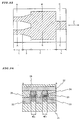
- Fig. 1 to Fig. 3 show a semiconductor laser according to a first embodiment of the present invention. Fig. 1 is a plan view of the semiconductor laser, Fig. 2 is a cross sectional view about the line A-A in Fig. 1, and Fig. 3 is a cross sectional view about the line B-B in Fig. 1. This semiconductor laser is a buried-heterostructure (BH) semiconductor laser having 1.55-micrometer band.
- As shown in Fig. 1, the semiconductor laser according to the present embodiment includes a first
multi-mode waveguide 2 formed in a multi-mode waveguide region and asingle mode waveguide 1 formed in a single mode waveguide region and coupled to a light incident end of the firstmulti-mode waveguide 2. - The first
multi-mode waveguide 2 formed in the multi-mode waveguide region is a multi-mode interference type waveguide having one input and one output (hereinafter, referred to as 1×1-MMI.). - As for the lengths of the respective regions, length of the
single mode waveguide 1 is about 50 micrometers, and length of the firstmulti-mode waveguide 2 is about 260 micrometers. The entire length of the semiconductor laser is about 310 micrometers. - As shown in Fig. 2 and Fig. 3, the semiconductor laser according to the present embodiment includes: an n-
InP substrate 21 having a protruded portion; an n-InP buffer layer 22, anactive layer 23, and a p-InPfirst cladding layer 24 which are formed in a mesa shape on the protruded portion of the n-InP substrate 21; a p-InPcurrent blocking layer 25 and an n-InPcurrent blocking layer 26 which are formed around themesa 30; and a p-InPsecond cladding layer 27 and a p+-InGaAs cap layer 28 which are formed on the p-InPfirst cladding layer 24 and the n-InPcurrent layer 26. - As shown in Fig. 2 and Fig. 3, the
active layer 23 is made from 1.55-micrometer composition InGaAsP. Theactive layer 23 has a current confinement structure surrounded by the p-InPcurrent blocking layer 25 and the n-Inpcurrent blocking layer 26, and is covered with the p-InPfirst cladding layer 24, the p-InPsecond cladding layer 27, and the p+-InGaAs cap layer 28. - As shown in Fig. 2 and Fig. 3, the p-InP
current blocking layer 25 and the n-InPcurrent blocking layer 26 are formed in such a way that only the p-InPcurrent blocking layer 25 is in contact with the side wall of themesa 30 and only the n-InPcurrent blocking layer 26 is in contact with the p-InPsecond cladding layer 27. - Comparison of Fig. 2 with Fig. 3 clarifies that the
single mode waveguide 1 is different from the firstmulti-mode waveguide 2 in width of the waveguide. As shown in Fig. 2, thesingle mode waveguide 1 has a waveguide width (W1) set to W1 = 2 micrometers. Moreover, as shown in Fig. 3, the firstmulti-mode waveguide 2 has a waveguide width (W2) set to W2 = 10 micrometers. - Hereinafter, referring to Fig. 4 to Fig. 7, explanation will be given on a production method of the semiconductor laser according to the present embodiment.
- Firstly, as shown in Fig. 4, the n-
InP substrate 21 is successively covered with the n-InP buffer layer 22, theactive layer 23 made from 1.55-micrometer composition InGaAsP, and the p-InPfirst cladding layer 24, using the metal organic vapor phase epitaxy (MOVPE) technique.
The respective layers have thickness values as follows: the n-InP buffer layer is set to about 100 nm, the 1.55-micrometer InGaAsPactive layer 23 is set to about 100 nm, and the p-InPfirst cladding layer 24 is set to about 100 nm.
Next, the ordinary photolithography method and wet etching method are used to form a mesa-shapingmask 31 on the p-InPfirst cladding layer 24. - Next, as shown in Fig. 5, the reactive ion etching (RIE) technique is used to remove a portion of the p-InP
first cladding layer 24, the 1.55-micrometer InGaAsPactive layer 23, the n-InP buffer layer 22, and the n-InP substrate 21, thus forming amesa 30. - Next, as shown in Fig. 6, using the MOVPE technique, the p-InP
current blocking layer 25 and the n-InPcurrent blocking layer 26 are formed around themesa 30. Thesecurrent blocking layer current blocking layer 25 is in contact with the side wall of themesa 30 and only the n-InPcurrent blocking layer 26 is exposed outside. - Each of the p-InP
current blocking layer 25 and the n-InPcurrent blocking layer 26 has a thickness of about 1 micrometer. - Next, the mesa-shaping
mask 31 is removed by buffered hydrofluoric acid. - After this, as shown in Fig. 7, the p-InP
first cladding layer 24 and the n-InPcurrent blocking layer 26 are covered with the p-InPsecond cladding layer 27 and then with the p+-InGaAs cap layer 28 using the MOVPE technique. - Next, the back surface of the n-
InP substrate 21 is polished. - Next, a rear electrode and a front electrode are formed using the ordinary sputtering method.
- After an element is cleaved, the cleaved facet of the side of the
single mode waveguide 1 is coated with an ordinary half reflection (HR) coating, and the cleaved facet of the light emitting side is coated with an anti-reflective (AR) coating. - Thus, production procedure of the embodied semiconductor laser according to the present embodiment is completed.
- The semiconductor laser according to the present embodiment is a laser oscillating a single mode, which can achieve a high output compared to a conventional single mode laser and improve the COD level. Furthermore the semiconductor laser according to the present embodiment can improve the spatial hole burning compared to a conventional laser having using a multi-mode waveguide having a flare structure. Moreover, the semiconductor laser has an excellent mode stability and does not cause efficiency lowering due to a mode conversion loss. Hereinafter, explanation will be given on the principle explaining these merits.
- The semiconductor laser according to the present embodiment, as shown in Fig. 1, is designed as 1×1-MMI. having the first
multi-mode waveguide 2. That is, the firstmulti-mode waveguide 2 is a quasi-single mode waveguide in which only the single mode light propagates at the both facets in spite of the multi-mode waveguide. - Fig. 8 and Fig. 9 show simulation results of configuration of the semiconductor laser according to the present embodiment using two-dimensional beam propagation technique. Fig. 8 shows a simulation result of the first
multi-mode waveguide 2 having the 1×1-MMI. configuration in the semiconductor laser according to the present embodiment. - Fig. 9 shows, for comparison, a simulation result of a multi-mode waveguide having a conventional flare structure.
- Referring to Fig. 8, single mode light which has propagated through the
single mode waveguide 1 is introduced into multi-mode in the region of the firstmulti-mode waveguide 2 and again identically imaged as a single mode at the end of the firstmulti-mode waveguide 2. - On the other hand, referring to Fig. 9, in the conventional multi-mode waveguide having the flare structure, the mode conversion of the single mode itself is performed as the single mode light advances in the waveguide and the single mode is output at the end.
- As shown in Fig. 8, if a regular single mode waveguide is coupled to one end of a multi-mode waveguide, oscillation is performed in a single mode even if the light output facet is constituted by a facet of the multi-mode waveguide.
- In such oscillation, the first
multi-mode waveguide 2 is a main pumping light region. This firstmulti-mode waveguide 2 is wider than thesingle mode waveguide 1 and accordingly, theactive layer 23 has an improved gain saturation level compared to the ordinary single mode semiconductor laser. Thus, it is possible to achieve a high output. - Moreover, in the semiconductor laser according to the present embodiment, the light output facet is also constituted by the wide first
multi-mode waveguide 2. - Accordingly, in comparison to the ordinary single mode semiconductor laser, the light density is lowered at the light output facet even if the same light intensity, which improves the COD level.
- Furthermore, in the semiconductor laser according to the present embodiment, the output mode can be controlled independently by the
single mode waveguide 1, and themulti-mode waveguide 2 formed as the 1×1-MMI. does not operate as 1×1-MMI. for odd modes according to the MMI. theory. That is, no odd modes are excited. Accordingly, the spatial hole burning is not easily caused in comparison to the conventional semiconductor laser utilizing the multi-mode waveguide having the flare shape as shown in Fig. 9. As a result, it is possible to realize a semiconductor laser having an excellent mode stability.
In addition to the aforementioned, the semiconductor laser according to the present embodiment uses themulti-mode waveguide 2 performing the MMI. operation and accordingly, no mode conversion loss is generated in principle. - Accordingly, the semiconductor laser according to the present embodiment does not cause efficiency lowering as is observed in the conventional semiconductor laser utilizing the flare structure.
- Moreover, the layer configuration of the semiconductor laser according to the present embodiment is equivalent to the layer configuration of an ordinary semiconductor laser and can be produced by the ordinary semiconductor laser production procedure. That is, the semiconductor laser according to the present embodiment can be produced comparatively easily by the established production method with a high reproducibility and a high yield.
- Moreover, the semiconductor laser of the present embodiment has a comparatively simple configuration and can easily be applied to an integrated optical device. It should be noted that the present (first) embodiment and the following second to eighth embodiments are assumed to have a simple buried-heterostructure. However, the embodiments are not to be limited to the buried-heterostructure and can be applied to the other layer configuration such as ridge structure or double channel planner buried-heterostructure (DC-PBH) having an excellent current confinement,
- Moreover, in the present embodiment, the laser wavelength is set to the 1.55-micrometer band but the laser wavelength is not to be limited to this value. For example, the laser wavelength may be in a visible light region or 0.98 micrometer band or other near infrared light band.
- Furthermore, the
active layer 23 in the present embodiment has a bulk structure, but theactive layer 23 can also have a multiple quantum well (MQW) structure. - Moreover, with respect to the production method, in the present embodiment and the second to the eighth embodiments which will be detailed later, the MOVPE technique is used for crystal growth and the RIE technique is used for formation of the
mesa 30. However, the production method is not to be limited to this. For example, the molecular beam epitaxy (MBE) method can be used for crystal growth and wet etching can be used for formation of themesa 30. - Fig. 10 to Fig. 12 show a semiconductor laser according to a second embodiment of the present invention. Fig. 10 is a plan view of the semiconductor laser according to the present embodiment, Fig. 11 is a cross sectional view about the line A-A in Fig. 10, and Fig. 12 is a cross sectional view about the line B-B in Fig. 10. The semiconductor laser according to the present embodiment is a buried-heterostructure (BH) type and has a 1.55-micrometer band.
- As shown in Fig. 10, the semiconductor laser according to the second embodiment includes: a first
multi-mode waveguide 2 formed in a multi-mode waveguide region; asingle mode waveguide 1 formed at the light incident side of the firstmulti-mode waveguide 2 in a single mode waveguide region; and atapered waveguide 3 connecting thesingle mode waveguide 1 to the first multimode waveguide2. - The first
multi-mode waveguide 2 formed in the multi-mode waveguide region is constituted as one input and one output type multi-mode interference type (1×1-MMI.). The respective regions have length as follows: length of thesingle mode waveguide 1 is about 50 micrometers, length of the firstmulti-mode waveguide 2 is about 260 micrometers, length of the taperedwaveguide 3 is about 50 micrometers, and the entire length of the semiconductor laser is about 360 micrometers. - As shown in Fig. 11 and Fig. 12, the semiconductor laser according to the present embodiment includes: an n-
InP substrate 21 having a protruding portion; an n-InP buffer layer 22, anactive layer 23, and a p-InPfirst cladding layer 24 which are formed in a mesa shape on the protruding portion of the n-InP substrate 21; a p-Inpcurrent blocking layer 25 and an n-InPcurrent blocking layer 26 layered around themesa 30; and a p-InPsecond cladding layer 27 and a p+-InGaAs cap layer 28 which are layered on the p-InPfirst cladding layer 24 and the n-InPcurrent blocking layer 26. As shown in Fig. 11 and Fig. 12, theactive layer 23 is made from 1.55-micrometer composition InGaAsP and has a current confinement structure defined by the p-InPcurrent blocking layer 25 and the n-InPcurrent blocking layer 26. Theactive layer 23 is covered by the p-InPfirst cladding layer 24, the p-InPsecond cladding layer 27 and the p+-InGaAs cap layer 28. - As shown in Fig. 11 and Fig. 12, the p-InP
current blocking layer 25 and the n-InPcurrent blocking layer 26 are formed in such a manner that only the p-InPcurrent blocking layer 25 is in contact with the side wall of themesa 30, and the only the n-InPcurrent blocking layer 26 is in contact with the p-InPsecond cladding layer 27. A comparison of Fig. 11 with Fig. 12 clarifies that the difference between thesingle mode waveguide 1 and the firstmulti-mode waveguide 2 is only the waveguide width. As shown in Fig. 11, thesingle mode waveguide 1 has a waveguide width (W1) set to W1 = 2 micrometers, and as shown in Fig. 12, the first multi-mode waveguide width (W2) is set to W2 = 10 micrometers. As for the taperedwaveguide 3, its width is 2 micrometers, i.e., identical to thesingle mode waveguide 1, at the end coupled to thesingle mode waveguide 1. and the width at the end coupled to the firstmulti-mode waveguide 2 is W3 = 3.5 micrometers. - The production method of the semiconductor laser according to the present embodiment is identical to the production method of the semiconductor laser according to the first embodiment.
- The semiconductor laser according to the present embodiment is a laser oscillating a single mode which can achieve a high output compared to a conventional single mode laser and improve the COD level. Furthermore, the semiconductor laser according to the present embodiment can improve the spatial hole burning compared to a conventional laser using a multi-mode waveguide having a flare structure. Moreover, the semiconductor laser has an excellent mode stability and does not cause efficiency lowering due to a mode conversion loss. Furthermore, the semiconductor laser according to the present embodiment can improve coupling efficiency with an optical fiber. Hereinafter, explanation will be given on the principle explaining these merits.
- As shown in Fig. 10, the semiconductor laser according to the present embodiment, compared to the semiconductor laser according to the first embodiment, has a tapered
waveguide region 3 between thesingle mode waveguide 1. and the firstmulti-mode waveguide 2. - Thus, like the first embodiment, the present embodiment has a structure including the
multi-mode waveguide 2 and accordingly, it is possible to improve the gain saturation level of theactive layer 23 compared to an ordinary single mode semiconductor laser. - Moreover, in the semiconductor laser according to the present embodiment, like in the first embodiment, the light output facet is constituted by the facet of the
multi-mode waveguide 2. This improves the COD (catastrophic optical damage) level compared to an ordinary semiconductor laser using a single mode waveguide. - Furthermore, in the semiconductor laser according to the present embodiment, its output mode can be controlled independently by the
single mode waveguide 1, and themulti-mode waveguide 2 formed as the 1×1-MMI. in this embodiment does not operate as the 1×1-MMI. for the odd mode according to the MMI. theory. That is, no odd modes are excited. - Accordingly, the spatial hole burning is not easily caused compared to the conventional semiconductor laser utilizing the multi-mode waveguide having the flare structure as shown in Fig. 9. This enables to realize a semiconductor laser having an excellent mode stability.
- In addition to the aforementioned, the semiconductor laser according to the present embodiment uses the
multi-mode waveguide 2 performing the MMI. operation and accordingly, no mode conversion loss is generated in principle. - Accordingly, the semiconductor laser according to the present embodiment does not cause efficiency lowering as is observed in the conventional semiconductor laser utilizing the flare structure.
- Furthermore, the semiconductor laser according to the present embodiment has such a structure that the tapered
waveguide 3 is inserted between thesingle mode waveguide 1 and themulti-mode waveguide 2. Accordingly, it is possible to reduce the coupling loss (through very little) between thesingle mode waveguide 1 and the firstmulti-mode waveguide 2 almost to 0 dB. - It should be noted that in the present embodiment, although the tapered
waveguide 3 is implemented, the region of thewaveguide 3 is very small. Accordingly, almost no mode conversion loss is caused and the mode stability can be maintained by the no odd mode pumping condition in the MMI. region. - Moreover, the tapered
waveguide 3 widens the optical field at the light output facet of themulti-mode waveguide 2. As a result, the coupling efficiency with the single mode optical fiber is improved. - Fig. 13 is a graphic view showing a far-field pattern of width W1 = 2 micrometers calculated when a light is emitted by the ordinary single mode waveguide, whereas Fig. 14 is a graphic view showing a far-field pattern calculated when light is emitted at the facet of the
multi-mode waveguide 2 coupled to the taperedwaveguide 3 according to the present embodiment. - A comparison of Fig. 13 with Fig. 14 clarifies that in the semiconductor laser according to the present embodiment, the half value width of the far-field pattern is improved from 24 degrees to 17 degrees. This improves the coupling loss with the single mode optical fiber by about 1 dB.
- Moreover, the layered configuration of the semiconductor laser according to the present embodiment is equivalent to the layered configuration of an ordinary semiconductor laser. Accordingly, like the first embodiment, the semiconductor laser according to the present embodiment can be produced by the same production procedure of the ordinary semiconductor laser. That is, the semiconductor laser according to the present embodiment can be produced comparatively easily by using only the established production method, i.e., with a high repeatability and yield.
- Moreover, since the semiconductor laser according to the present embodiment has a comparatively simple configuration, it can also be applied to an integrated optical device.
- Fig. 15 to Fig. 17 show a semiconductor laser according to a third embodiment of the present invention. Fig. 15 is a plan view of the semiconductor laser according to the present embodiment, Fig. 16 is a cross sectional view about the line A-A in Fig. 15, and Fig. 17 is a cross sectional view about the line B-B in Fig. 15. The semiconductor laser according to the present embodiment has a buried heterostructure (BH) with a 1.55-micrometer band.
- As shown in Fig. 15, the semiconductor laser according to the present embodiment includes a first
multi-mode waveguide 2 formed in a multi-mode waveguide region and asingle mode waveguide 1 formed in a single mode waveguide region and coupled to the light incident end of the firstmulti-mode waveguide 2. - The first
multi-mode waveguide 2 formed in the multi-mode waveguide region is formed as a 1×2-MMI.. Thesingle mode waveguide 1 has a length of about 50 micrometers, the firstmulti-mode waveguide 2 has a length of about 460 micrometers, and the entire length of the semiconductor laser is about 510 micrometers. - As shown in Fig. 16 and Fig. 17, the semiconductor laser according to the present embodiment includes: an n-
InP substrate 21 having a protruding portion; an n-InP buffer layer 22, anactive layer 23, and a p-InPfirst cladding layer 24 which are formed in a mesa shape on the protruding portion of the n-InP substrate 21; a p-Inpcurrent blocking layer 25 and an n-InPcurrent blocking layer 26 layered around themesa 30; and a p-InPsecond cladding layer 27 and a p+-InGaAs cap layer 28 which are layered on the p-InPfirst cladding layer 24 and the n-InPcurrent blocking layer 26. - As shown in Fig. 16 and Fig. 17, the
active layer 23 is made from 1.55-micrometer composition InGaAsP and has a current confinement structure defined by the p-InPcurrent blocking layer 25 and the n-InPcurrent blocking layer 26. Theactive layer 23 is covered by the p-InPfirst cladding 24, the p-InPsecond cladding layer 27 and the p+-InGaAs cap layer 28. - As shown in Fig. 16 and Fig. 17, the p-InP
current blocking layer 25 and the n-InPcurrent blocking layer 26 are formed in such a manner that only the p-InPcurrent blocking layer 25 is in contact with the side wall of themesa 30, and the only the n-InP current blocking layer is in contact with the p-InPsecond cladding layer 27. - A comparison of Fig. 16 with Fig. 17 clarifies that the difference between the
single mode waveguide 1 and the firstmulti-mode waveguide 2 is only the waveguide width. As shown in Fig. 16, thesingle mode waveguide 1 has a waveguide width (W1) set to W1 = 2 micrometers, and as shown in Fig. 17, the first multi-mode waveguide width (W2) is set to W2 = 20 micrometers. - The production method of the semiconductor laser according to the present embodiment is identical to the production method of the semiconductor laser according to the first embodiment.
- The semiconductor laser according to the present embodiment is a laser oscillating a single mode, which can achieve a high output compared to a conventional single mode laser and improve the COD. Furthermore, the semiconductor laser according to the present embodiment can improve the spatial hole burning compared to a conventional laser using a multi-mode waveguide having a flare structure. Moreover. the semiconductor laser has an excellent mode stability and does not cause efficiency lowering due to a mode conversion loss. Hereinafter, explanation will be given on the principle explaining these merits.
- In the semiconductor laser according to the present embodiment, the first
multi-mode waveguide 2 is designed as a 1×2-MMI.. Moreover, the firstmulti-mode waveguide 2 is connected to twosingle mode waveguides 1. Accordingly, at the other facet, i.e., the light output end of the firstmulti-mode waveguide 2, it is possible to obtain a single mode oscillation. - Thus, like the first embodiment, the present embodiment has a structure including the
multi-mode waveguide 2 and accordingly, it is possible to improve the gain saturation level of theactive layer 23 compared to an ordinary single mode semiconductor laser. - Moreover, in the semiconductor laser according to the present embodiment, like in the first embodiment, the light output facet is constituted by the facet of the
multi-mode waveguide 2. This improves the COD (catastrophic optical damage) level compared to an ordinary semiconductor laser using a single mode waveguide. - Furthermore, in the semiconductor laser according to the present embodiment, its output mode can be controlled independently by the
single mode waveguide 1, and in this embodiment no odd mode is caused. Accordingly, the spatial hole burning is not easily caused compared to the conventional semiconductor laser utilizing the multi-mode waveguide having the flare structure as shown in Fig. 9. This enables to realize a semiconductor laser having an excellent mode stability. - In addition to the aforementioned, the semiconductor laser according to the present embodiment uses the
multi-mode waveguide 2 performing the MMI. operation and accordingly, no mode conversion loss is generated in principle. - Accordingly, the semiconductor laser according to the present embodiment does not cause efficiency lowering as is observed in the conventional semiconductor laser utilizing the flare structure.
- Moreover, the layered configuration of the semiconductor laser according to the present embodiment is equivalent to the layered configuration of an ordinary semiconductor laser. Accordingly, like the first embodiment, the semiconductor laser according to the present embodiment can be produced by the same production procedure of the ordinary semiconductor laser. That is, the semiconductor laser according to the present embodiment can be produced by using only the established production method, i.e., with a high repeatability and yield.
- Moreover, since the semiconductor laser according to the present embodiment has a comparatively simple configuration, it can also be applied to an integrated optical device.
- Fig. 18 to Fig. 20 show a semiconductor laser according to a fourth embodiment of the present invention. Fig. 18 is a plan view of the semiconductor laser according to the present embodiment, Fig. 19 is a cross sectional view about the line A-A in Fig. 18, and Fig. 20 is a cross sectional view about the line B-B in Fig. 18. The semiconductor laser according to the present embodiment is a buried-heterostructure (BH) type and has a 1.55-micrometer band.
- As shown in Fig. 18, the semiconductor laser according to the present embodiment includes: a first
multi-mode waveguide 2 formed in a multi-mode waveguide region; asingle mode waveguide 1 formed at the light incident end of the firstmulti-mode waveguide 2, in a single mode waveguide region; and atapered waveguide 3 coupling the firstmulti-mode waveguide 2 to thesingle mode waveguide 1. - The first
multi-mode waveguide 2 formed in the multi-mode waveguide region is constituted as 1×2-MMI.. The respective regions have length as follows: thesingle mode waveguide 1 is about 50 micrometers long, the firstmulti-mode waveguide 2 is about 460 micrometers, the taperedwaveguide 3 is about 50 micrometers, and the entire length of the semiconductor laser is about 560 micrometers. As shown in Fig. 19 and Fig. 20, the semiconductor laser according to the present embodiment includes: an n-InP substrate 21 having a protruding portion; an n-InP buffer layer 22, anactive layer 23, and a p-InPfirst cladding layer 24 which are formed in a mesa shape on the protruding portion of the n-InP substrate 21; a p-InPcurrent blocking layer 25 and an n-InPcurrent blocking layer 26 layered around themesa 30; and p-InPsecond cladding layer 27 and p+-InGaAs cap layer 28 which are layered on the p-InPfirst cladding layer 24 and the n-InPcurrent blocking layer 26. - As shown in Fig. 19 and Fig. 20, the
active layer 23 is made from 1.55-micrometer composition InGaAsP and has a current confinement structure defined by the p-InPcurrent blocking layer 25 and the n-InPcurrent blocking layer 26. Theactive layer 23 is covered by the p-InPfirst cladding layer 24, the p-InPsecond cladding layer 27 and the p+-InGaAs cap layer 28. - As shown in Fig. 19 and Fig. 20. the p-InP
current blocking layer 25 and the n-InPcurrent blocking layer 26 are formed in such a manner that only the p-InPcurrent blocking layer 25 is in contact with the side wall of themesa 30, and the only the n-InP current blocking layer is in contact with the p-InPsecond cladding layer 27.
A comparison of Fig. 19 with Fig. 20 clarifies that the difference between thesingle mode waveguide 1 and the firstmulti-mode waveguide 2 is only the waveguide width. As shown in Fig. 19, thesingle mode waveguide 1 has a waveguide width (W1) set to W1 = 2 micrometers, and as shown in Fig. 20, the firstmulti-mode waveguide 2 width (W2) is set to W2 = 20 micrometers. As for the taperedwaveguide 3, its width is 2 micrometers, i.e., identical to thesingle mode waveguide 1, at the end coupled to thesingle mode waveguide 1 and the width at the end coupled to the firstmulti-mode waveguide 2 is W3 = 3.5 micrometers. - The production method of the semiconductor laser according to the present embodiment is identical to the production method of the semiconductor laser according to the first embodiment.
- The semiconductor laser according to the present embodiment is a laser oscillating a single mode, which can achieve a high output compared to a conventional single mode laser and improve the COD level. Furthermore, the semiconductor laser according to the present embodiment can improve the spatial hole burning compared to a conventional laser using a multi-mode waveguide having a flare structure. Moreover, the semiconductor laser has an excellent mode stability and does not cause efficiency lowering due to a mode conversion loss. Furthermore, the semiconductor laser according to the present embodiment can improve coupling efficiency with an optical fiber. Hereinafter, explanation will be given on the principle explaining these merits. In the semiconductor laser according to the present embodiment, like in the third embodiment, the first
multi-mode waveguide 2 is designed as 1×2-MMI.. Moreover, the firstmulti-mode waveguide 2 is connected to twosingle mode waveguides 1 via taperedwaveguides 3. Accordingly, at the other facet of the firstmulti-mode waveguide 2, i.e., at the light output facet, it is possible to obtain a single mode oscillation. - The semiconductor laser according to the present embodiment, like the first embodiment, has a structure including the
multi-mode waveguide 2 and accordingly, it is possible to improve the gain saturation level of theactive layer 23 compared to an ordinary single mode semiconductor laser. - Moreover, in the semiconductor laser according to the present embodiment, like in the first embodiment, the light output facet is constituted by the facet of the
multi-mode waveguide 2. This improves the COD (catastrophic optical damage) level compared to an ordinary semiconductor laser using a single mode waveguide. - Furthermore, in the semiconductor laser according to the present embodiment, its output mode can be controlled independently by the
single mode waveguide 1, and no odd modes are excited. Accordingly, the spatial hole burning is not easily caused compared to the conventional semiconductor laser utilizing the multi-mode waveguide having the flare structure. This enables to realize a semiconductor laser having an excellent mode stability. - In addition to the aforementioned, the semiconductor laser according to the present embodiment uses the
multi-mode waveguide 2 performing the MMI. operation and accordingly, no mode conversion loss is generated in principle. - Accordingly, the semiconductor laser according to the present embodiment does not cause efficiency lowering as is observed in the conventional semiconductor laser utilizing the flare structure.
- Furthermore, the semiconductor laser according to the present embodiment has such a structure that the tapered
waveguide 3 is inserted between thesingle mode waveguide 1 and themulti-mode waveguide 2. Accordingly, it is possible to reduce the coupling loss (through very little) between thesingle mode waveguide 1 and the firstmulti-mode waveguide 2 almost to 0 dB. - It should be noted that in the present embodiment, although the tapered
waveguide 3 is implemented, the region of thewaveguide 3 is very small. Accordingly, almost no mode conversion loss is caused and the mode stability can be maintained by the no odd mode pumping condition in the MMI. region. - Moreover, the tapered
waveguide 3 widens the optical field at the light output facet of themulti-mode waveguide 2. As a result, the coupling efficiency with the single mode optical fiber is improved. - Moreover, the layered configuration of the semiconductor laser according to the present embodiment is equivalent to the layered configuration of an ordinary semiconductor laser. Accordingly, like the first embodiment, the semiconductor laser according to the present embodiment can be produced by the same production procedure of the ordinary semiconductor laser. That is, the semiconductor laser according to the present embodiment can be produced comparatively easily by using only an established production method, i.e., with a high repeatability and yield. Moreover, since the semiconductor laser according to the present embodiment has a comparatively simple configuration, it can also be applied to an integrated optical device.
- Fig. 21 to Fig. 24 show a semiconductor laser according to a fifth embodiment of the present invention. Fig. 21 is a plan view of the semiconductor laser according to the present embodiment, Fig. 22 is a cross sectional view about the line A-A in Fig. 21, Fig. 23 is a cross sectional view about the line B-B in Fig. 21, and Fig. 24 is a cross sectional view about the line C-C in Fig 21. The semiconductor laser according to the present embodiment is a buried-heterostructure (BH) type and has a 1.55-micrometer band.
- As shown in Fig. 21, the semiconductor laser according to the present embodiment includes: a first
multi-mode waveguide 2 formed in a multi-mode waveguide region; asingle mode waveguide 1 formed at in a single mode waveguide region; atapered waveguide 3 connecting thesingle mode waveguide 1 to the firstmulti-mode waveguide 2; and a secondmulti-mode waveguide 4 formed to be coupled to the firstmulti-mode waveguide 2 at the light incident side of the firstmulti-mode waveguide 2. - The first
multi-mode waveguide 2 formed in the multi-mode waveguide region is constituted as a one-input one-output interference type waveguide (1×1-MMI.). Moreover, the secondmulti-waveguide region 4 is designed as a secondary mode cleaved waveguide. - The respective regions have length as follows: the
single mode waveguide 1 has a length of about 50 micrometers, the firstmulti-mode waveguide 2 has a length of about 260 micrometers, the taperedwaveguide 3 has a length of about 50 micrometers, the secondmulti-mode waveguide 4 has a length of about 50 micrometers, and the entire length of the semiconductor laser is about 410 micrometers. - As shown in Fig. 22 to Fig. 24, the semiconductor laser according to the present embodiment includes: an n-
InP substrate 21 having a protruding portion; an n-InP buffer layer 22, anactive layer 23, and a p-InPfirst cladding layer 24 which are formed in a mesa shape on the protruding portion of the n-InP substrate 21; a p-InPcurrent blocking layer 25 and an n-InPcurrent blocking layer 26 layered around themesa 30; and p-InPsecond cladding layer 27 and p+-InGaAs cap layer 28 which are layered on the p-InPfirst cladding layer 24 and the n-InPcurrent blocking layer 26. - As shown in Fig. 22 to Fig. 24, the
active layer 23 is made from 1.55-micrometer composition InGaAsP and has a current confinement structure defined by the p-InPcurrent blocking layer 25 and the n-InPcurrent blocking layer 26. - The
active layer 23 is covered by the p-InPfirst cladding layer 24, the p-InPsecond cladding layer 27 and the p+-InGaAs cap layer 28. - As shown in Fig. 22 to Fig. 24, the p-InP
current blocking layer 25 and the n-InPcurrent blocking layer 26 are formed in such a manner that only the p-InPcurrent blocking layer 25 is in contact with the side wall of themesa 30, and the only the n-InPcurrent blocking layer 26 is in contact with the p-InPsecond cladding layer 27. - A comparison of Fig. 22 with Fig. 23 and Fig. 24 clarifies that the difference between the
single mode waveguide 1, the firstmulti-mode waveguide 2, and the secondmulti-mode waveguide 4 is only the waveguide width. As shown in Fig. 22, thesingle mode waveguide 1 has a waveguide width (W1) set to W1 = 2 micrometers, and as shown in Fig. 23, the firstmulti-mode waveguide 2 width (W2) is set to W2 = 10 micrometers. As for the taperedwaveguide 3, its width is 2 micrometers, i.e., identical to thesingle mode waveguide 1, at the end coupled to thesingle mode waveguide 1 and the width at the end coupled to the firstmulti-mode waveguide 2 is W3 = 3.5 micrometers. Moreover, as shown in Fig. 24, the secondmulti-mode waveguide 4 has a width (W4) set to W4 = 3.5 micrometers. - The production method of the semiconductor laser according to the present embodiment is identical to the production method of the semiconductor laser according to the first embodiment.
- The semiconductor laser according to the present embodiment is a laser oscillating a single mode, which can achieve a high output compared to a conventional single mode laser and improve the COD level. Furthermore, the semiconductor laser according to the present embodiment can improve the spatial hole burning compared to a conventional laser using a multi-mode waveguide having a flare structure. Moreover, the semiconductor laser according to the present embodiment has an excellent mode stability and does not cause efficiency lowering due to a mode conversion loss.
- Furthermore, the semiconductor laser according to the present embodiment can improve coupling efficiency with an optical fiber. Hereinafter, explanation will be given on the principle explaining these merits.
- The semiconductor laser according to the present embodiment is identical to the semiconductor laser according to the second embodiment except for that the second
multi-mode region 4 is added. - Thus, the semiconductor laser according to the present embodiment includes the
multi-mode waveguide 2 like the second embodiment and accordingly, can improve the gain saturation level of theactive layer 23 compared to an ordinary single mode semiconductor laser.
Moreover, in the semiconductor laser according to the present embodiment, like in the first embodiment, the light output facet is constituted by the facet of the secondmulti-mode waveguide 4 which is the multi-mode waveguide. This improves the COD (catastrophic optical damage) level compared to an ordinary semiconductor laser using a single mode waveguide. Furthermore, in the semiconductor laser according to the present embodiment, its output mode can be controlled independently by thesingle mode waveguide 1, and themulti-mode waveguide 2 formed as 1×1-MMI., according to the MMI. theory, does not operate 1×1-MMI. for the odd modes. That is, no odd modes are excited. Accordingly, the spatial hole burning is not easily caused compared to the conventional semiconductor laser utilizing the multi-mode waveguide having the flare structure as shown in Fig. 9. This enables to realize a semiconductor laser having an excellent mode stability. - In addition to the aforementioned, the semiconductor laser according to the present embodiment uses the
multi-mode waveguides - Furthermore, the semiconductor laser according to the present embodiment has such a structure that the tapered
waveguide 3 is inserted between thesingle mode waveguide 1 and the firstmulti-mode waveguide 2. Accordingly, it is possible to reduce the coupling loss (though very little) between thesingle mode waveguide 1 and the firstmulti-mode waveguide 2 almost to 0 dB. - It should be noted that in the present embodiment, although the tapered
waveguide 3 is implemented, the region of thewaveguide 3 is very small. Accordingly, almost no mode conversion loss is caused and the mode stability can be maintained by the no odd mode pumping condition in the MMI. region. - Moreover, the tapered
waveguide 3 widens the optical field at the light output facet of themulti-mode waveguide 2. As a result, the coupling efficiency with the single mode optical fiber is improved. - Moreover, in the semiconductor laser according to the present embodiment, the light output facet is constituted by the second mode cleaved waveguide (second multi-mode waveguide) 4 which is different from the first
multi-mode waveguide 2 in which the light output facet is a main pumping region. Accordingly, the tolerance for the cutting position is mitigated, facilitating a production procedure. It should be noted that since the firstmulti-mode waveguide 2 is designed in such a manner that no odd modes are excited. - Accordingly, even if the second
multi-mode waveguide 4 is used as a waveguide of the output side, only the single mode is output without deteriorating the mode stability. Moreover, the layered configuration of the semiconductor laser according to the present embodiment is equivalent to the layered configuration of an ordinary semiconductor laser. Accordingly, like the first embodiment, the semiconductor laser according to the present embodiment can be produced by the same production procedure of the ordinary semiconductor laser. That is, the semiconductor laser according to the present embodiment can be produced comparatively easily by using only an established production method, i.e., with a high repeatability and yield. Moreover, since the semiconductor laser according to the present embodiment has a comparatively simple configuration, it can also be applied to an integrated optical device. - Fig. 25 to Fig. 28 show a semiconductor laser according to a sixth embodiment of the present invention. Fig. 25 is a plan view of the semiconductor laser according to the present embodiment, Fig. 26 is a cross sectional view about the line A-A in Fig. 25, Fig. 27 is a cross sectional view about the line B-B in Fig. 25, and Fig. 28 is a cross sectional view about the line C-C in Fig 25. The semiconductor laser according to the present embodiment is a buried-heterostructure (BH) type and has a 1.55-micrometer band.
- As shown in Fig. 25, the semiconductor laser according to the present embodiment includes: a first
multi-mode waveguide 2 formed in a multi-mode waveguide region; asingle mode waveguide 1 formed in a single mode waveguide region; atapered waveguide 3 connecting the single mode waveguide to the firstmultimode waveguide 2; and a secondmulti-mode waveguide 4 formed to be coupled to the firstmulti-mode waveguide 2 at the light incident side of the firstmulti-mode waveguide 2. - The first
multi-mode waveguide 2 formed in the multi-mode waveguide region is constituted as 1×2-MMI.. Moreover, the secondmulti-waveguide region 4 is designed as a secondary mode cleaved waveguide. - The respective regions have length as follows: the
single mode waveguide 1 has a length of about 50 micrometers, the firstmulti-mode waveguide 2 has a length of about 460 micrometers, the taperedwaveguide 3 has a length of about 50 micrometers, the secondmulti-mode waveguide 4 has a length of about 50 micrometers, and the entire length of the semiconductor laser is about 610 micrometers. - As shown in Fig. 25 to Fig. 28, the semiconductor laser according to the present embodiment includes: an n-
InP substrate 21 having a protruding portion; an n-InP buffer layer 22, anactive layer 23, and a p-InPfirst cladding layer 24 which are formed in a mesa shape on the protruding portion of the n-InP substrate 21; a p-InPcurrent blocking layer 25 and an n-InPcurrent blocking layer 26 layered around themesa 30; and p-InPsecond cladding layer 27 and p+-InGaAs cap layer 28 which are layered on the p-InPfirst cladding layer 24 and the n-InPcurrent blocking layer 26. - As shown in Fig. 25 to Fig. 28, the
active layer 23 is made from 1.55-micrometer composition InGaAsP and has a current confinement structure defined by the p-InPcurrent blocking layer 25 and the n-InPcurrent blocking layer 26. Theactive layer 23 is covered by the p-InPfirst cladding layer 24, the p-InPsecond cladding layer 27 and the p+-InGaAs cap layer 28. - As shown in Fig. 26 to Fig. 28, the p-InP
current blocking layer 25 and the n-InPcurrent blocking layer 26 are formed in such a manner that only the p-InPcurrent blocking layer 25 is in contact with the side wall of themesa 30, and the only the n-InP current blocking layer is in contact with the p-InPsecond cladding layer 27. - A comparison of Fig. 26 with Fig. 27 and Fig. 28 clarifies that the difference between the
single mode waveguide 1, the firstmulti-mode waveguide 2, and the secondmulti-mode waveguide 4 is only the waveguide width. As shown in Fig. 26, thesingle mode waveguide 1 has a waveguide width (W1) set to W1 = 2 micrometers, and as shown in Fig. 27, the firstmulti-mode waveguide 2 width (W2) is set to W2 = 20 micrometers. As for the taperedwaveguide 3, its width is 2 micrometers, i.e., identical to thesingle mode waveguide 1, at the end coupled to thesingle mode waveguide 1 and the width at the end coupled to the firstmulti-mode waveguide 2 is W3 = 3.5 micrometers. Moreover, as shown in Fig. 28, the secondmulti-mode waveguide 4 has a width (W4) set to W4 = 3.5 micrometers. - The production method of the semiconductor laser according to the present embodiment is identical to the production method of the semiconductor laser according to the first embodiment.
- The semiconductor laser according to the present embodiment is a laser oscillating a single mode, which can achieve a high output compared to a conventional single mode laser and improve the COD level. Furthermore, the semiconductor laser according to the present embodiment can improve the spatial hole burning compared to a conventional laser using a multi-mode waveguide having a flare structure. Moreover, the semiconductor laser according to the present embodiment has an excellent mode stability and does not cause efficiency lowering due to a mode conversion loss.
- Furthermore, the semiconductor laser according to the present embodiment can improve coupling efficiency with an optical fiber. Hereinafter, explanation will be given on the principle explaining these merits.
- The semiconductor laser according to the present embodiment is identical to the semiconductor laser according to the fourth embodiment except for that the second
multi-mode region 4 is added. - Thus, the semiconductor laser according to the present embodiment includes the
multi-mode waveguide 2 like the fourth embodiment and accordingly, can improve the gain saturation level of theactive layer 23 compared to an ordinary single mode semiconductor laser. - Moreover, in the semiconductor laser according to the present embodiment, like in the fourth embodiment, the light output facet is constituted by the facet of the second
multi-mode waveguide 4. This improves the COD (catastrophic optical damage) level compared to an ordinary semiconductor laser using a single mode waveguide. - Furthermore, in the semiconductor laser according to the present embodiment, its output mode can be controlled independently by the
single mode waveguide 1, and no odd modes are excited. Accordingly, the spatial hole burning is not easily caused compared to the conventional semiconductor laser utilizing the multi-mode waveguide having the flare structure. This enables to realize a semiconductor laser having an excellent mode stability. - In addition to the aforementioned, the semiconductor laser according to the present embodiment uses the
multi-mode waveguides - Furthermore, the semiconductor laser according to the present embodiment has such a structure that the tapered
waveguide 3 is inserted between thesingle mode waveguide 1 and the firstmulti-mode waveguide 2. Accordingly, it is possible to reduce the coupling loss (though very little) between thesingle mode waveguide 1 and the firstmulti-mode waveguide 2 almost to 0 dB. - It should be noted that in the present embodiment, although the tapered
waveguide 3 is implemented, the region of thewaveguide 3 is very small. Accordingly, almost no mode conversion loss is caused and the mode stability can be maintained by the no odd mode pumping condition in the MMI. region. - Moreover, the tapered
waveguide 3 widens the optical field at the light output facet of themulti-mode waveguide 2. As a result, the coupling efficiency with the single mode optical fiber is improved. - Moreover, in the semiconductor laser according to the present embodiment, the light output facet is constituted by the second mode cleaved waveguide (second multi-mode waveguide) 4 which is different from the first
multi-mode waveguide 2 in which the light output facet is a main pumping region. Accordingly, the tolerance for the cutting position is mitigated, facilitating a production procedure. - It should be noted that since the first
multi-mode waveguide 2 is designed in such a manner that no odd modes are excited. Accordingly, even if the secondmulti-mode waveguide 4 is used as a waveguide of the output side, only the single mode is output without deteriorating the mode stability. - Moreover, the layered configuration of the semiconductor laser according to the present embodiment is equivalent to the layered configuration of an ordinary semiconductor laser. Accordingly, like the first embodiment, the semiconductor laser according to the present embodiment can be produced by the same production procedure of the ordinary semiconductor laser. That is, the semiconductor laser according to the present embodiment can be produced comparatively easily by using only an established production method, i.e., with a high repeatability and yield.
- Moreover, since the semiconductor laser according to the present embodiment has a comparatively simple configuration, it can also be applied to an integrated optical device.
- Fig. 29 to Fig. 32 show a semiconductor laser according to a seventh embodiment of the present invention. Fig. 29 is a plan view of the semiconductor laser according to the present embodiment, Fig. 30 is a cross sectional view about the line A-A in Fig. 29, Fig. 31 is a cross sectional view about the line B-B in Fig. 29, and Fig. 32 is a cross sectional view about the line C-C in Fig 29. The semiconductor laser according to the present embodiment is a buried-heterostructure (BH) type and has a 1.55-micrometer band.
- As shown in Fig. 29, the semiconductor laser according to the present embodiment includes: a first
multi-mode waveguide 2 formed in a multi-mode waveguide region; asingle mode waveguide 1 formed at in a single mode waveguide region; atapered waveguide 3 connecting thesingle mode waveguide 1 to the firstmultimode waveguide 2; and a secondmulti-mode waveguide 4 connected to the firstmulti-mode waveguide 2. Each of the firstmulti-mode waveguide 2 and thesecond multi-waveguide 4 is designed as a 1×1-MMI.. - The respective regions have length as follows: the
single mode waveguide 1 has a length of about 50 micrometers, the firstmulti-mode waveguide 2 has a length of about 260 micrometers, the taperedwaveguide 3 has a length of about 50 micrometers, the secondmulti-mode waveguide 4 has a length of about 75 micrometers, and the entire length of the semiconductor laser is about 435 micrometers. - As shown in Fig. 30 to Fig. 32, the semiconductor laser according to the present embodiment includes: an n-
InP substrate 21 having a protruding portion; an n-InP buffer layer 22, anactive layer 23, and a p-InPfirst cladding layer 24 which are formed in a mesa shape on the protruding portion of the n-InP substrate 21; a p-InPcurrent blocking layer 25 and an n-InPcurrent blocking layer 26 layered around themesa 30; and p-InPsecond cladding layer 27 and p+-InGaAs cap layer 28 which are layered on the p-InPfirst cladding layer 24 and the n-InPcurrent blocking layer 26. - As shown in Fig. 30 to Fig. 32, the
active layer 23 is made from 1.55-micrometer composition InGaAsP and has a current confinement structure defined by the p-InPcurrent blocking layer 25 and the n-InPcurrent blocking layer 26. Theactive layer 23 is covered by the p-InPfirst cladding layer 24, the p-InPsecond cladding layer 27 and the p+-InGaAs cap layer 28. - As shown in Fig. 30 to Fig. 32, the p-InP
current blocking layer 25 and the n-InPcurrent blocking layer 26 are formed in such a manner that only the p-InPcurrent blocking layer 25 is in contact with the side wall of themesa 30, and the only the n-InPcurrent blocking layer 26 is in contact with the p-InPsecond cladding layer 27. - A comparison of Fig. 30 with Fig. 31 and Fig. 32 clarifies that the difference between the
single mode waveguide 1, the firstmulti-mode waveguide 2, and the secondmulti-mode waveguide 4 is only the waveguide width. As shown in Fig. 30, thesingle mode waveguide 1 has a waveguide width (W1) set to W1 = 2 micrometers, and as shown in Fig. 31, the firstmulti-mode waveguide 2 width (W2) is set to W2 = 10 micrometers. As for the taperedwaveguide 3, its width is 2 micrometers, i.e. identical to thesingle mode waveguide 1, at the end coupled to thesingle mode waveguide 1 and the width at the end coupled to the firstmulti-mode waveguide 2 is W3 = 3.5 micrometers. - Moreover, as shown in Fig. 32, the second
multi-mode waveguide 4 has a width (W4) set to W4 = 5 micrometers. This secondmulti-mode waveguide 4 is a multi-mode waveguide allowing the second mode and this secondmulti-mode waveguide 4 has a length of 75 micrometers, thus realizing the 1×1-MMI structure. - The production method of the semiconductor laser according to the present embodiment is identical to the production method of the semiconductor laser according to the first embodiment.
- The semiconductor laser according to the present embodiment is a laser oscillating a single mode, which can achieve a high output compared to a conventional single mode laser and improve the COD level. Furthermore, the semiconductor laser according to the present embodiment can improve the spatial hole burning compared to a conventional laser using a multi-mode waveguide having a flare structure. Moreover, the semiconductor laser according to the present embodiment has an excellent mode stability and does not cause efficiency lowering due to a mode conversion loss. Furthermore; the semiconductor laser according to the present embodiment can improve coupling efficiency with an optical fiber. Hereinafter, explanation will be given on the principle explaining these merits.
- The semiconductor laser according to the present embodiment is identical to the semiconductor laser according to the second embodiment except for that the second
multi-mode region 4 is added. - Thus, the semiconductor laser according to the present embodiment includes the
multi-mode waveguide 2 like the second embodiment and accordingly, can improve the gain saturation level of theactive layer 23 compared to an ordinary single mode semiconductor laser. - Moreover, in the semiconductor laser according to the present embodiment, like in the first embodiment, the light output facet is constituted by the facet of the second
multi-mode waveguide 4 which is a multi-mode waveguide. This improves the COD (catastrophic optical damage) level compared to an ordinary semiconductor laser using a single mode waveguide. - Furthermore, in the semiconductor laser according to the present embodiment, its output mode can be controlled independently by the
single mode waveguide 1, and no odd modes are excited. Accordingly, the spatial hole burning is not easily caused compared to the conventional semiconductor laser utilizing the multi-mode waveguide having the flare structure. This enables to realize a semiconductor laser having an excellent mode stability. - In addition to the aforementioned, the semiconductor laser according to the present embodiment uses the
multi-mode waveguides - Furthermore, the semiconductor laser according to the present embodiment has such a structure that the tapered
waveguide 3 is inserted between thesingle mode waveguide 1 and the firstmulti-mode waveguide 2. Accordingly, it is possible to reduce the coupling loss (though very little) between thesingle mode waveguide 1 and the firstmulti-mode waveguide 2 almost to 0 dB. - It should be noted that in the present embodiment, although the tapered
waveguide 3 is implemented, the region of thewaveguide 3 is very small. Accordingly, almost no mode conversion loss is caused and the mode stability can be maintained by the no odd mode pumping condition in the MMI. region. - Moreover, the tapered
waveguide 3 widens the optical field at the light output facet of themulti-mode waveguide 2. As a result, the coupling efficiency with the single mode optical fiber is improved. - Moreover, in the semiconductor laser according to the present embodiment, the light output facet is constituted by the waveguide of 1×1-MMI. structure (the second multi-mode waveguide) 4 which is different from the first
multi-mode waveguide 2 in which the light output facet is a main pumping region. Accordingly, the tolerance for the cutting position is mitigated, facilitating a production procedure. - It should be noted that since the first
multi-mode waveguide 2 is designed in such a manner that no odd modes are excited. Accordingly, even if the secondmulti-mode waveguide 4 is used as a waveguide of the output side, only the single mode is output without deteriorating the mode stability. - Moreover, the layered configuration of the semiconductor laser according to the present embodiment is equivalent to the layered configuration of an ordinary semiconductor laser. Accordingly, like the first embodiment, the semiconductor laser according to the present embodiment can be produced by the same production procedure of the ordinary semiconductor laser. That is, the semiconductor laser according to the present embodiment can be produced comparatively easily by using only an established production method, i.e., with a high repeatability and yield.
- Moreover, since the semiconductor laser according to the present embodiment has a comparatively simple configuration, it can also be applied to an integrated optical device.
- Fig. 33 to Fig. 36 show a semiconductor laser according to an eighth embodiment of the present invention. Fig. 33 is a plan view of the semiconductor laser according to the present embodiment, Fig. 34 is a cross sectional view about the line A-A in Fig. 33, Fig. 35 is a cross sectional view about the line B-B in Fig. 33, and Fig. 36 is a cross sectional view about the line C-C in Fig 33. The semiconductor laser according to the present embodiment is a buried-heterostructure (BH) type and has a 1.55-micrometer band.
- As shown in Fig. 33, the semiconductor laser according to the present embodiment includes: a first
multi-mode waveguide 2 formed in a multi-mode waveguide region; asingle mode waveguide 1 formed in a single mode waveguide region; atapered waveguide 3 connecting thesingle mode waveguide 1 to the firstmultimode waveguide 2; and a secondmulti-mode waveguide 4 connected to the firstmulti-mode waveguide 2. - The first
multi-mode waveguide 2 formed in the multi-mode waveguide region is designed as 1×2-MMI.. Moreover, thesecond multi-waveguide 4 is designed as a 1 ×1-MMI.. - The respective regions have length as follows: the
single mode waveguide 1 has a length of about 50 micrometers, the firstmulti-mode waveguide 2 has a length of about 460 micrometers, the taperedwaveguide 3 has a length of about 50 micrometers, the secondmulti-mode waveguide 4 has a length of about 75 micrometers, and the entire length of the semiconductor laser is about 635 micrometers. - As shown in Fig. 34 to Fig. 36, the semiconductor laser according to the present embodiment includes: an n-
InP substrate 21 having a protruding portion; an n-InP buffer layer 22, anactive layer 23, and a p-InPfirst cladding layer 24 which are formed in a mesa shape on the protruding portion of the n-InP substrate 21; a p-InPcurrent blocking layer 25 and an n-InPcurrent blocking layer 26 layered around themesa 30; and p-InPsecond cladding layer 27 and p+-InGaAs cap layer 28 which are layered on the p-InPfirst cladding layer 24 and the n-InPcurrent blocking layer 26. - As shown in Fig. 34 to Fig. 36, the
active layer 23 is made from 1.55-micrometer composition InGaAsP and has a current confinement structure defined by the p-InPcurrent blocking layer 25 and the n-InPcurrent blocking layer 26. - The
active layer 23 is covered by the p-InPfirst cladding layer 24, the p-InPsecond cladding layer 27 and the p+-InGaAs cap layer 28. - As shown in Fig. 34 to Fig. 36, the p-InP
current blocking layer 25 and the n-InPcurrent blocking layer 26 are formed in such a manner that only the p-InPcurrent blocking layer 25 is in contact with the side wall of themesa 30, and the only the n-InPcurrent blocking layer 26 is in contact with the p-InPsecond cladding layer 27. - A comparison of Fig. 34 with Fig. 35 and Fig. 36 clarifies that the difference between the
single mode waveguide 1, the firstmulti-mode waveguide 2, and the secondmulti-mode waveguide 4 is only the waveguide width. As shown in Fig. 34, thesingle mode waveguide 1 has a waveguide width (W1) set to W1 = 2 micrometers, and as shown in Fig. 35, the firstmulti-mode waveguide 2 width (W2) is set to W2 = 20 micrometers. As for the taperedwaveguide 3, its width is 2 micrometers, i.e., identical to thesingle mode waveguide 1, at the end coupled to thesingle mode waveguide 1 and the width at the end coupled to the firstmulti-mode waveguide 2 is W3 = 3.5 micrometers. - Moreover, as shown in Fig. 36, the second
multi-mode waveguide 4 has a width (W4) set to W4 = 5 micrometers. This secondmulti-mode waveguide 4 is a multi-mode waveguide allowing the second mode and this secondmulti-mode waveguide 4 has a length of 75 micrometers, thus realizing the 1×1-MMI. structure. - The production method of the semiconductor laser according to the present embodiment is identical to the production method of the semiconductor laser according to the first embodiment.
- The semiconductor laser according to the present embodiment is a laser oscillating a single mode, which can achieve a high output compared to a conventional single mode laser and improve the COD level. Furthermore, the semiconductor laser according to the present embodiment can improve the spatial hole burning compared to a conventional laser having using a multi-mode waveguide having a flare structure. Moreover, the semiconductor laser according to the present embodiment has an excellent mode stability and does not cause efficiency lowering due to a mode conversion loss. Furthermore, the semiconductor laser according to the present embodiment can improve coupling efficiency with an optical fiber. Hereinafter, explanation will be given on the principle explaining these merits.
- The semiconductor laser according to the present embodiment is identical to the semiconductor laser according to the fourth embodiment except for that the second
multi-mode region 4 is added. - Thus, the semiconductor laser according to the present embodiment includes the
multi-mode waveguide 2 like the fourth embodiment and accordingly, can improve the gain saturation level of theactive layer 23 compared to an ordinary single mode semiconductor laser. - Moreover, in the semiconductor laser according to the present embodiment, like in the fourth embodiment, the light output facet is constituted by the facet of the second
multi-mode waveguide 4. This improves the COD (catastrophic optical damage) level compared to an ordinary semiconductor laser using a single mode waveguide. - Furthermore, in the semiconductor laser according to the present embodiment, its output mode can be controlled independently by the
single mode waveguide 1, and no odd modes are excited. Accordingly, the spatial hole burning is not easily caused compared to the conventional semiconductor laser utilizing the multi-mode waveguide having the flare structure. This enables to realize a semiconductor laser having an excellent mode stability.
In addition to the aforementioned, the semiconductor laser according to the present embodiment uses themulti-mode waveguides - Furthermore, the semiconductor laser according to the present embodiment has such a structure that the tapered
waveguide 3 is inserted between thesingle mode waveguide 1 and the firstmulti-mode waveguide 2. Accordingly, it is possible to reduce the coupling loss (though very little) between thesingle mode waveguide 1 and the firstmulti-mode waveguide 2 almost to 0 dB. - Moreover, the tapered
waveguide 3 widens the optical field at the light output facet of themulti-mode waveguide 2. As a result, the coupling efficiency with the single mode optical fiber is improved. - Moreover, in the semiconductor laser according to the present embodiment, the light output facet is constituted by the waveguide of 1×1-MMI structure (the second multi-mode waveguide) 4 which is different from the first
multi-mode waveguide 2. Accordingly, the tolerance for the cutting position is mitigated, facilitating a production procedure. - It should be noted that since the first
multi-mode waveguide 2 is designed in such a manner that no odd modes are excited. Accordingly, even if the secondmulti-mode waveguide 4 is used as a waveguide of the output side, only the single mode is output without deteriorating the mode stability. - Moreover, the layered configuration of the semiconductor laser according to the present embodiment is equivalent to the layered configuration of an ordinary semiconductor laser. Accordingly, like the first embodiment, the semiconductor laser according to the present embodiment can be produced by the same production procedure of the ordinary semiconductor laser. That is, the semiconductor laser according to the present embodiment can be produced comparatively easily by using only an established production method, i.e., with a high repeatability and yield. Moreover, since the semiconductor laser according to the present embodiment has a comparatively simple configuration, it can also be applied to an integrated optical device.
- Fig. 37 to Fig. 39 show a semiconductor optical amplifier according to an ninth embodiment of the present invention. Fig. 37 is a plan view of the semiconductor optical amplifier according to the present embodiment, Fig. 38 is a cross sectional view about the line A-A in Fig. 37, and Fig. 39 is a cross sectional view about the line B-B in Fig. 37. The semiconductor optical amplifier according to the present embodiment is a buried-heterostructure (BH) type and has a 1.55-micrometer band.
- As shown in Fig. 37, the semiconductor optical amplifier according to the present embodiment includes: a first
multi-mode waveguide 2 formed in a multi-mode waveguide region; and asingle mode waveguide 1 formed in a single mode waveguide region, which is connected to the firstmulti-mode waveguide 2. - The first
multi-mode waveguide 2 formed in the multi-mode waveguide region is designed as 1×1-MMI.. The respective regions have length as follows: thesingle mode waveguide 1 has a length of about 50 micrometers, and the firstmulti-mode waveguide 2 has a length of about 260 micrometers. The entire length of the semiconductor laser (sic) is about 310 micrometers. - As shown in Fig. 38 and Fig. 39, the semiconductor optical amplifier according to the present embodiment includes: an n-
InP substrate 21 having a protruding portion; an n-InP buffer layer 22, anactive layer 23, and a p-InPfirst cladding layer 24 which are formed in a mesa shape on the protruding portion of the n-InP substrate 21; a p-InPcurrent blocking layer 25 and an n-InPcurrent blocking layer 26 layered around themesa 30; and p-InPsecond cladding layer 27 and p+-InGaAs cap layer 28 which are layered on the p-InPfirst cladding layer 24 and the n-InPcurrent blocking layer 26. - As shown in Fig. 38 and Fig. 39, the
active layer 23 is made from 1.55-micrometer composition InGaAsP and has a current confinement structure defined by the p-InPcurrent blocking layer 25 and the n-InPcurrent blocking layer 26. - The
active layer 23 is covered by the p-InPfirst cladding layer 24, the p-InPsecond cladding layer 27 and the p+-InGaAs cap layer 28. - As shown in Fig. 38 and Fig. 39, the p-InP
current blocking layer 25 and the n-InPcurrent blocking layer 26 are formed in such a manner that only the p-InPcurrent blocking layer 25 is in contact with the side wall of themesa 30, and the only the n-InPcurrent block layer 26 is in contact with the p-InPsecond cladding layer 27. - A comparison of Fig. 38 with Fig. 39 clarifies that the difference between the
single mode waveguide 1 and the firstmulti-mode waveguide 2 is only the waveguide width. As shown in Fig. 38, thesingle mode waveguide 1 has a waveguide width (W1) set to W1 = 2 micrometers, and as shown in Fig. 39, the firstmulti-mode waveguide 2 width (W2) is set to W2 = 10 micrometers. - Hereinafter, referring to Fig. 4 to Fig. 7, explanation will be given on a production method of the semiconductor optical amplifier according to the present embodiment. Firstly, as shown in Fig. 4, the n-
InP substrate 21 is successively covered with the n-InP buffer layer 22, theactive layer 23 made from 1.55-micrometer composition InGaAsP, and the p-InPfirst cladding layer 24, using the MOVPE technique. - The respective layers have thickness values as follows: the n-InP buffer layer is set to about 100 nm, the 1.55-micrometer InGaAsP
active layer 23 is set to about 100 nm, and the p-InPfirst cladding layer 24 is set to about 100 nm. - Next, the ordinary photolithography technique and wet etching method are used to form a mesa-shaping
mask 31 on the p-InPfirst cladding layer 24. - Next, as shown in Fig. 5, the reactive ion etching (RIE) technique is used to remove a portion of the p-InP
first cladding layer 24, the 1.55-micrometer InGaAsPactive layer 23, the n-InP buffer layer 22, and the n-InP substrate 21, thus forming amesa 30. - Next, as shown in Fig. 6, using the MOVPE technique, the p-InP
current blocking layer 25 and the n-InPcurrent blocking layer 26 are formed around themesa 30. Thesecurrent blocking layer current blocking layer 25 is in contact with the side wall of the mesa and only the n-InPcurrent blocking layer 26 is exposed outside. - Each of the p-InP
current blocking layer 25 and the n-InPcurrent blocking layer 26 has a thickness of about 1 micrometer. - Next, the mesa-shaping
mask 31 is removed by buffered hydrofluoric acid. - After this, as shown in Fig. 7, the p-InP
first cladding layer 24 and the n-InPcurrent blocking layer 26 are covered with the p-InPsecond cladding layer 27 and then with the p+-InGaAs cap layer 28 using the MOVPE technique. Next, the back surface of the n-InP substrate 21 is polished. Next, a rear electrode and a front electrode are formed using the ordinary sputtering method. - After an element is cleaved, the cleaved facet is coated with an anti-reflective (AR) coating. Thus, production procedure of the embodied semiconductor laser according to the present embodiment is completed.
- The semiconductor optical amplifier according to the present embodiment is a semiconductor optical amplifier for outputting a single mode, which can achieve a high gain and high saturation output compared to a conventional single mode optical amplifier and improve the COD level. Furthermore the semiconductor optical amplifier according to the present embodiment can improve the spatial hole burning compared to a conventional laser using a multi-mode waveguide having a flare structure. Moreover, the semiconductor optical amplifier has an excellent mode stability and does not cause efficiency lowering due to a mode conversion loss.
- Hereinafter, explanation will be given on the principle explaining these merits.
- As shown in Fig. 37, the semiconductor optical amplifier according to the present embodiment is designed as a 1×1-MMI. having a first
multi-mode waveguide 2. That is, the firstmulti-mode waveguide 2 is a quasi-single mode waveguide, i.e., although being a multi-mode waveguide, only a single mode light propagates at the both ends. - Thus, the semiconductor optical amplifier includes a multi-mode waveguide, which improves a gain saturation level of the
active layer 23, achieving a high saturation gain and a high saturation output compared to an ordinary single mode semiconductor optical amplifier. - Moreover, in the semiconductor optical amplifier according to the present embodiment, its light output facet is constituted by the wide first
multi-mode waveguide 2. - Accordingly, when compared to an ordinary single mode semiconductor laser, the light density at the light output facet is reduced for the same light output, thus improving the COD level.
- Furthermore, in the semiconductor optical amplifier according to the present embodiment, its output mode can be controlled independently by the
single mode waveguide 1 and structurally no odd modes are excited. Accordingly the spatial hole burning is not easily generated compared to the conventional semiconductor optical amplifier. Thus, it is possible to realize a semiconductor optical amplifier having an excellent mode stability. - Additionally, since the semiconductor optical amplifier according to the present embodiment employs the
multi-mode waveguide 2 performing the MMI. operation, no mode conversion loss is generated in principle. Accordingly, the effect lowering observed in the conventional semiconductor optical amplifier is not caused. - Moreover, the layered configuration of the semiconductor optical amplifier according to the present embodiment is equivalent to the layered configuration of an ordinary semiconductor optical amplifier. Accordingly, the semiconductor optical amplifier according to the present embodiment can be produced by the same production procedure of the ordinary semiconductor optical amplifier. That is, the semiconductor optical amplifier according to the present embodiment can be produced comparatively easily by using only the established production method, i.e., with a high repeatability and yield.
- Moreover, since the semiconductor optical amplifier according to the present embodiment has a comparatively simple configuration, it can also be applied to an integrated optical device.
It should be noted that in the present embodiment and in a tenth to twelfth embodiment which will be detailed later, the semiconductor optical amplifier has a simple buried-heterostructure (BH structure). However, the present embodiment and the tenth to twelfth embodiment are not to be limited to the buried-heterostructure. For example, the present embodiment and the tenth to twelfth embodiment can be applied to a ridge structure or DC-PBH structure having an excellent current confinement.
Moreover, in the present embodiment, the laser wavelength is set to a 1.55-micrometer band but not to be limited to this band. For example, the laser wavelength may be a visible light band or a 0.98-micrometer band or other near infrared light band.
Furthermore, theactive layer 23 in the present embodiment has a bulk structure, but theactive layer 23 may have a multi-quantum well (MQW) structure.
As for the production method, in the present embodiment and the tenth to twelfth embodiment, the MOVPE technique is used for crystal growth and the RIE technique is used for formation of themesa 30. However, the embodiments are not to be limited to these techniques. For example, the MBE technique can used for the crystal growth and the wet etching can be used for formation of themesa 30. - Fig. 40 to Fig. 42 show a semiconductor optical amplifier according to a tenth embodiment of the present invention. Fig. 40 is a plan view of the semiconductor optical amplifier according to the present embodiment. Fig. 41 is a cross sectional view about the line A-A 9 in Fig. 40 and Fig. 42 is a cross sectional view about the line B-B in Fig. 40. The semiconductor optical amplifier according to the present embodiment has a buried-heterostructure (BH) and a 1.55-micrometer band.
As shown in Fig. 40, the semiconductor optical amplifier according to the present embodiment includes: a firstmulti-mode waveguide 2 formed in a multi-mode waveguide region; asingle mode waveguide 1 formed at the light incident side of the firstmulti-mode waveguide 2 in a single mode waveguide region; and atapered waveguide 3 connecting thesingle mode waveguide 2 to the firstmultimode waveguide 2. - The first
multi-mode waveguide 2 formed in the multi-mode waveguide region is constituted as 1×1-MMI.. The respective regions have length as follows: length of thesingle mode waveguide 1 is about 50 micrometers, length of the firstmulti-mode waveguide 2 is about 260 micrometers, length of the taperedwaveguide 3 is about 50 micrometers, and the entire length of the semiconductor optical amplifier is about 360 micrometers. - As shown in Fig. 41 and Fig. 42, the semiconductor optical amplifier according to the present embodiment includes: an n-
InP substrate 21 having a protruding portion; an n-InP buffer layer 22, anactive layer 23, and a p-InPfirst cladding layer 24 which are formed in a mesa shape on the protruding portion of the n-InP substrate 21; a p-Inpcurrent blocking layer 25 and an n-InPcurrent blocking layer 26 layered around themesa 30; and a p-InPsecond cladding layer 27 and a p+-InGaAs cap layer 28 which are layered on the p-InPfirst cladding layer 24 and the n-InPcurrent blocking layer 26. - As shown in Fig. 41 and Fig. 42, the
active layer 23 is made from 1.55-micrometer composition InGaAsP and has a current confinement structure defined by the p-InPcurrent blocking layer 25 and the n-InPcurrent blocking layer 26. Theactive layer 23 is covered by the p-InPfirst cladding layer 24, the p-InPsecond cladding layer 27 and the p+-InGaAs cap layer 28. - As shown in Fig. 41 and Fig. 42, the p-InP
current blocking layer 25 and the n-InPcurrent blocking layer 26 are formed in such a manner that only the p-InPcurrent blocking layer 25 is in contact with the side wall of themesa 30, and the only the n-InPcurrent blocking layer 26 is in contact with the p-InPsecond cladding layer 27. - A comparison of Fig. 41 with Fig. 42 clarifies that the difference between the
single mode waveguide 1 and the firstmulti-mode waveguide 2 is only the waveguide width. As shown in Fig. 41, thesingle mode waveguide 1 has a waveguide width (W1) set to W1 = 2 micrometers, and as shown in Fig. 42, the firstmulti-mode waveguide 2 width (W2) is set to W2 = 10 micrometers. As for the tapered waveguide, its width is 2 micrometers, i.e., identical to thesingle mode waveguide 1, at the end coupled to thesingle mode waveguide 1 and the width at the end coupled to the firstmulti-mode waveguide 2 is W3 = 3.5 micrometers. - The production method of the semiconductor optical amplifier according to the present embodiment is identical to the production method of the semiconductor optical amplifier according to the ninth embodiment. The semiconductor optical amplifier according to the present embodiment is a optical amplifier outputting a single mode which can achieve a high output compared to a conventional single mode optical amplifier and improve the COD level.
- Furthermore, the semiconductor optical amplifier according to the present embodiment can improve the spatial hole burning compared to a conventional optical amplifier using a multi-mode waveguide having a flare structure.
- Moreover, the semiconductor optical amplifier has an excellent mode stability and does not cause efficiency lowering due to a mode conversion loss. Hereinafter, explanation will be given on the principle explaining these merits.
- As shown in Fig. 40, the semiconductor optical amplifier according to the present embodiment, compared to the semiconductor optical amplifier according to the ninth embodiment, has a tapered
waveguide region 3 between thesingle mode waveguide 1 and the firstmulti-mode waveguide 2. Accordingly, the firstmulti-mode waveguide 2, although being a multi-mode waveguide, constitutes a quasi-single mode waveguide in which only a single mode light propagates at the both facets. - Thus, like the ninth embodiment, the semiconductor optical amplifier according to the present embodiment has a structure including the
multi-mode waveguide 2 and accordingly, it is possible to improve the gain saturation level of theactive layer 23 compared to an ordinary single mode semiconductor optical amplifier. As a result, it is possible to obtain a high saturation gain and a high saturation output. - Moreover, in the semiconductor optical amplifier according to the present embodiment, like in the ninth embodiment, the light output facet is constituted by the facet of the
multi-mode waveguide 2. This improves the COD (catastrophic optical damage) level compared to an ordinary semiconductor optical amplifier using a single mode waveguide. - Furthermore, in the semiconductor optical amplifier according to the present embodiment, its output mode can be controlled independently by the
single mode waveguide 1, and structurally no odd modes are excited. Accordingly, the spatial hole burning is not easily caused compared to the conventional semiconductor optical amplifier utilizing the multi-mode waveguide having the flare structure. This enables to realize a semiconductor optical amplifier having an excellent mode stability. - In addition to the aforementioned, the semiconductor optical amplifier according to the present embodiment uses the
multi-mode waveguide 2 performing the MMI. operation and accordingly, no mode conversion loss is generated in principle. Accordingly, the semiconductor optical amplifier according to the present embodiment does not cause efficiency lowering as is observed in the conventional semiconductor optical amplifier utilizing the flare structure. Furthermore, the semiconductor optical amplifier according to the present embodiment has such a structure that the taperedwaveguide 3 is inserted between thesingle mode waveguide 1 and themulti-mode waveguide 2. Accordingly, it is possible to reduce the coupling loss (though very little) between thesingle mode waveguide 1 and the firstmulti-mode waveguide 2 almost to 0 dB. - It should be noted that in the present embodiment, although the tapered
waveguide 3 is implemented, the region of thewaveguide 3 is very small. Accordingly, almost no mode conversion loss is caused and the mode stability can be maintained by the no odd mode pumping condition in the MMI. region. - Moreover, the tapered
waveguide 3 widens the optical field at the light output facet of themulti-mode waveguide 2. As a result, the coupling efficiency with the single mode optical fiber is improved. - Moreover, the layered configuration of the semiconductor optical amplifier according to the present embodiment is equivalent to the layered configuration of an ordinary semiconductor optical amplifier. Accordingly, like the ninth embodiment, the semiconductor optical amplifier according to the present embodiment can be produced by the same production procedure of the ordinary semiconductor optical amplifier. That is, the semiconductor optical amplifier according to the present embodiment can be produced comparatively easily by using only the established production method, i.e., with a high repeatability and yield. Moreover, since the semiconductor optical amplifier according to the present embodiment has a comparatively simple configuration, it can also be applied to an integrated optical device.
- Fig. 43 to Fig. 46 show a semiconductor optical amplifier according to an eleventh embodiment of the present invention. Fig. 43 is a plan view of the semiconductor optical amplifier according to the present embodiment, Fig. 44 is a cross sectional view about the line A-A in Fig. 43, Fig. 45 is a cross sectional view about the line B-B in Fig. 43, and Fig. 46 is a cross sectional view about the line C-C in Fig 43. The semiconductor optical amplifier according to the present embodiment is a buried-heterostructure (BH) type and has a 1.55-micrometer band.
- As shown in Fig. 43, the semiconductor optical amplifier according to the present embodiment includes: a first
multi-mode waveguide 2 formed in a multi-mode waveguide region; asingle mode waveguide 1. formed at in a single mode waveguide region; atapered waveguide 3 connecting thesingle mode waveguide 1 to the firstmultimode waveguide 2. - The first
multi-mode waveguide 2 formed in the multi-mode waveguide region is constituted as a 1×1-MMI.. Moreover, the secondmulti-waveguide region 4 is designed as a secondary mode cleaved waveguide. - The respective regions have length as follows: the
single mode waveguide 1 has a length of about 50 micrometers, the firstmulti-mode waveguide 2 has a length of about 260 micrometers, the taperedwaveguide 3 has a length of about 50 micrometers, the secondmulti-mode waveguide 4 has a length of about 50 micrometers, and the entire length of the semiconductor optical amplifier is about 410 micrometers. - As shown in Fig. 44 to Fig. 46, the semiconductor optical amplifier according to the present embodiment includes: an n-
InP substrate 21 having a protruding portion; an n-InP buffer layer 22, anactive layer 23, and a p-InPfirst cladding layer 24 which are formed in a mesa shape on the protruding portion of the n-InP substrate 21; a p-InPcurrent blocking layer 25 and an n-InPcurrent blocking layer 26 layered around themesa 30; and p-InPsecond cladding layer 27 and p+-InGaAs cap layer 28 which are layered on the p-InPfirst cladding layer 24 and the n-InPcurrent blocking layer 26. - As shown in Fig. 44 to Fig. 46, the
active layer 23 is made from 1.55-micrometer composition InGaAsP and has a current confinement structure defined by the p-InPcurrent blocking layer 25 and the n-InPcurrent blocking layer 26. - The
active layer 23 is covered by the p-InPfirst cladding layer 24, the p-InPsecond cladding layer 26 and the p+-InGaAs cap layer. - As shown in Fig. 44 to Fig. 46, the p-InP current blocking layer and the n-InP current blocking layer are formed in such a manner that only the p-InP
current blocking layer 25 is in contact with the side wall of themesa 30, and the only the n-InP current blocking layer is in contact with the p-InPsecond cladding layer 27. - A comparison of Fig. 44 with Fig. 45 and Fig. 46 clarifies that the difference between the
single mode waveguide 1, the firstmulti-mode waveguide 2, and the second multi-mode waveguide is only the waveguide width. As shown in Fig. 44, thesingle mode waveguide 1 has a waveguide width (W1) set to W1 = 2 micrometers, and as shown in Fig. 45, the first multi-mode waveguide width (W2) is set to W2 = 10 micrometers. As for the taperedwaveguide 3, its width is 2 micrometers, i.e., identical to thesingle mode waveguide 1, at the end coupled to thesingle mode waveguide 1 and the width at the end coupled to the firstmulti-mode waveguide 2 is W3 = 3.5 micrometers. Moreover, as shown in Fig. 46, the secondmulti-mode waveguide 4 has a width (W4) set to W4 = 3.5 micrometers. - The production method of the semiconductor optical amplifier according to the present embodiment is identical to the production method of the semiconductor optical amplifier according to the ninth embodiment.
The semiconductor optical amplifier according to the present embodiment is a optical amplifier oscillating a single mode, which can achieve a high gain and a high saturation output compared to a conventional single mode optical amplifier and improve the COD level. Furthermore, the semiconductor optical amplifier according to the present embodiment can improve the spatial hole burning compared to a conventional semiconductor optical amplifier using a multi-mode waveguide having a flare structure. Moreover, the semiconductor optical amplifier according to the present embodiment has an excellent mode stability and does not cause efficiency lowering due to a mode conversion loss. Hereinafter, explanation will be given on the principle explaining these merits. - The semiconductor optical amplifier according to the present embodiment is identical to the semiconductor optical amplifier according to the tenth embodiment except for that the second
multi-mode region 4 is added.
Thus, like the tenth embodiment, the firstmulti-mode waveguide 2, being a multi-mode waveguide, serves as a quasi-single mode waveguide in which only the single mode light propagates at the both facets. - Thus, the semiconductor optical amplifier according to the present embodiment, like the tenth embodiment, includes the
multi-mode waveguide 2 and accordingly, can improve the gain saturation level of theactive layer 23 compared to an ordinary single mode semiconductor optical amplifier. As a result, it is possible to obtain a high saturation gain and a high saturation output. - Moreover, in the semiconductor optical amplifier according to the present embodiment, like in the ninth embodiment, the light output facet is constituted by the facet of the
multi-mode waveguide 2. This improves the COD (catastrophic optical damage) level compared to an ordinary semiconductor optical amplifier using a single mode waveguide. - Furthermore, in the semiconductor optical amplifier according to the present embodiment, its output mode can be controlled independently by the
single mode waveguide 1, and structurally no odd modes are excited. Accordingly, the spatial hole burning is not easily caused compared to the conventional semiconductor optical amplifier utilizing the multi-mode waveguide having the flare structure as shown. This enables to realize a semiconductor optical amplifier having an excellent mode stability. - In addition to the aforementioned, the semiconductor optical amplifier according to the present embodiment uses the
multi-mode waveguides - Furthermore, the semiconductor optical amplifier according to the present embodiment has such a structure that the tapered
waveguide 3 is inserted between thesingle mode waveguide 1 and the firstmulti-mode waveguide 2. Accordingly, it is possible to reduce the coupling loss (though very little) between thesingle mode waveguide 1 and the firstmulti-mode waveguide 2 almost to 0 dB. - It should be noted that in the present embodiment. although the tapered
waveguide 3 is implemented, the region of thewaveguide 3 is very small. Accordingly, almost no mode conversion loss is caused and the mode stability can be maintained by the no odd mode pumping condition in the MMI. region. - Moreover, the tapered
waveguide 3 widens the optical field at the light output facet of themulti-mode waveguide 2. As a result, the coupling efficiency with the single mode optical fiber is improved. - Moreover, in the semiconductor optical amplifier according to the present embodiment, the light output facet is constituted by the second mode cleaved waveguide (second multi-mode waveguide) 4 which is different from the first
multi-mode waveguide 2. Accordingly, the tolerance for the cutting position is mitigated, facilitating a production procedure. - It should be noted that since the first
multi-mode waveguide 2 is designed in such a manner that no odd modes are excited. Accordingly, even if the secondmulti-mode waveguide 4 is used as a waveguide of the output side, only the single mode is output without deteriorating the mode stability. - Moreover, the layered configuration of the semiconductor optical amplifier according to the present embodiment is equivalent to the layered configuration of an ordinary semiconductor laser. Accordingly, like the ninth embodiment, the semiconductor optical amplifier according to the present embodiment can be produced by the same production procedure of the ordinary semiconductor laser.
- That is, the semiconductor laser according to the present embodiment can be produced comparatively easily by using only an established production method, i.e., with a high repeatability and yield.
- Moreover, since the semiconductor optical amplifier according to the present embodiment has a comparatively simple configuration, it can also be applied to an integrated optical device.
- Fig. 47 to Fig. 50 show a semiconductor optical amplifier according to a twelfth embodiment of the present invention. Fig. 47 is a plan view of the semiconductor laser according to the present embodiment, Fig. 48 is a cross sectional view about the line A-A in Fig. 47, Fig. 49 is a cross sectional view about the line B-B in Fig. 47, and Fig. 50 is a cross sectional view about the line C-C in Fig 47. The semiconductor optical amplifier according to the present embodiment is a buried-heterostructure (BH) type and has a 1.55-micrometer band.
- As shown in Fig. 47, the semiconductor optical amplifier according to the present embodiment includes: a first
multi-mode waveguide 2 formed in a multi-mode waveguide region; asingle mode waveguide 1 formed at in a single mode waveguide region; atapered waveguide 3 connecting thesingle mode waveguide 2 to the firstmultimode waveguide 2; and a secondmulti-mode waveguide 4 formed to be coupled to the firstmulti-mode waveguide 2 at the light incident side of the firstmulti-mode waveguide 2. - Each of the first
multi-mode waveguide 2 and thesecond multi-waveguide 4 is designed as a 1×1-MMI.
The respective regions have length as follows: thesingle mode waveguide 1 has a length of about 50 micrometers, the firstmulti-mode waveguide 2 has a length of about 260 micrometers, the taperedwaveguide 3 has a length of about 50 micrometers, the secondmulti-mode waveguide 4 has a length of about 75 micrometers, and the entire length of the semiconductor optical amplifier is about 435 micrometers. As shown in Fig. 48 to Fig. 50, the semiconductor optical amplifier according to the present embodiment includes: an n-InP substrate 21 having a protruding portion; an n-InP buffer layer 22, anactive layer 23, and a p-InPfirst cladding layer 24 which are formed in a mesa shape on the protruding portion of the n-InP substrate 21; a p-InPcurrent blocking layer 25 and an n-InPcurrent blocking layer 26 layered around themesa 30; and p-InPsecond cladding layer 27 and p+-InGaAs cap layer 28 which are layered on the p-InPfirst cladding layer 24 and the n-InPcurrent blocking layer 26. - As shown in Fig. 48 to Fig. 50, the
active layer 23 is made from 1.55-micrometer composition InGaAsP and has a current confinement structure defined by the p-InPcurrent blocking layer 25 and the n-InPcurrent blocking layer 26. Theactive layer 23 is covered by the p-InPfirst cladding layer 24, the p-InPsecond cladding layer 27 and the p+-InGaAs cap layer. - As shown in Fig. 48 to Fig. 50, the p-InP
current blocking layer 25 and the n-InPcurrent blocking layer 26 are formed in such a manner that only the p-InPcurrent blocking layer 25 is in contact with the side wall of themesa 30, and the only the n-InP current blocking layer is in contact with the p-InPsecond cladding layer 27. - A comparison of Fig. 48 with Fig. 49 and Fig. 50 clarifies that the difference between the
single mode waveguide 1, the firstmulti-mode waveguide 2, and the second multi-mode waveguide is only the waveguide width. As shown in Fig. 48, thesingle mode waveguide 1 has a waveguide width (W1) set to W1 = 2 micrometers, and as shown in Fig. 49, the firstmulti-mode waveguide 2 width (W2) is set to W2 = 10 micrometers. As for the taperedwaveguide 3, its width is 2 micrometers, i.e. identical to thesingle mode waveguide 1, at the end coupled to thesingle mode waveguide 1 and the width at the end coupled to the firstmulti-mode waveguide 2 is W3 = 3.5 micrometers. - Moreover, as shown in Fig. 50, the second
multi-mode waveguide 4 has a width (W4) set to W4 = 5 micrometers. This secondmulti-mode waveguide 4 is a multi-mode waveguide allowing the second mode and this secondmulti-mode waveguide 4 has a length of 75 micrometers, thus realizing the 1×1-MMI structure. - The production method of the semiconductor optical amplifier according to the present embodiment is identical to the production method of the semiconductor optical amplifier according to the ninth embodiment.
The semiconductor optical amplifier according to the present embodiment is a laser oscillating a single mode, which can achieve a high output compared to a conventional single mode optical amplifier and improve the COD level. Furthermore, the semiconductor optical amplifier according to the present embodiment can improve the spatial hole burning compared to a conventional laser (sic) using a multi-mode waveguide having a flare structure. Moreover, the semiconductor optical amplifier according to the present embodiment has an excellent mode stability and does not cause efficiency lowering due to a mode conversion loss. Furthermore, the semiconductor optical amplifier according to the present embodiment can improve coupling efficiency with an optical fiber. Hereinafter, explanation will be given on the principle explaining these merits. - The semiconductor optical amplifier according to the present embodiment is identical to the semiconductor optical amplifier according to the tenth embodiment except for that the second
multi-mode region 4 is added. - Accordingly, like the tenth embodiment, the first
multi-mode waveguide 2, being a multi-mode waveguide, serves as a quasi-single mode waveguide in which only a single mode light propagates at the both facets. - Thus, like the tenth embodiment, the semiconductor laser according to the present embodiment includes the
multi-mode waveguide 2 and accordingly, can improve the gain saturation level of theactive layer 23 compared to an ordinary single mode semiconductor laser. As a result, it is possible to obtain a high saturation gain and a high saturation output. - Moreover, in the semiconductor laser according to the present embodiment, like in the ninth embodiment, the light output facet is constituted by the facet of the
multi-mode waveguide 2. This improves the COD (catastrophic optical damage) level compared to an ordinary semiconductor optical amplifier using a single mode waveguide. - Furthermore, in the semiconductor optical amplifier according to the present embodiment, its output mode can be controlled independently by the
single mode waveguide 1, and structurally no odd modes are excited. Accordingly, the spatial hole burning is not easily caused compared to the conventional semiconductor optical amplifier utilizing the multi-mode waveguide having the flare structure. This enables to realize a semiconductor optical amplifier having an excellent mode stability. - In addition to the aforementioned, the semiconductor optical amplifier according to the present embodiment uses the
multi-mode waveguides - Furthermore, the semiconductor optical amplifier according to the present embodiment has such a structure that the tapered
waveguide 3 is inserted between thesingle mode waveguide 1 and the firstmulti-mode waveguide 2. Accordingly, it is possible to reduce the coupling loss (though very little) between thesingle mode waveguide 1 and the firstmulti-mode waveguide 2 almost to 0 dB.
It should be noted that in the present embodiment, although the taperedwaveguide 3 is implemented, the region of thewaveguide 3 is very small. Accordingly, almost no mode conversion loss is caused and the mode stability can be maintained by the no odd mode pumping condition in the MMI. region. - Moreover, the tapered
waveguide 3 widens the optical field at the light output facet of themulti-mode waveguide 2. As a result, the coupling efficiency with the single mode optical fiber is improved. - Moreover, in the semiconductor optical amplifier according to the present embodiment, the light output facet is constituted by a secondary mode cleaved waveguide (second multi-mode waveguide) 4 which is different from the first
multi-mode waveguide 2 in which the light output facet is the main pumping region. Accordingly, the tolerance for the cutting position is mitigated, facilitating a production procedure. - It should be noted that since the first
multi-mode waveguide 2 is designed in such a manner that no odd modes are excited. Accordingly, even if the secondmulti-mode waveguide 4 is used as a waveguide of the output side, only the single mode is output without deteriorating the mode stability. - Moreover, the layered configuration of the semiconductor optical amplifier according to the present embodiment is equivalent to the layered configuration of an ordinary semiconductor optical amplifier. Accordingly, like the ninth embodiment, the semiconductor optical amplifier according to the present embodiment can be produced by the same production procedure of the ordinary semiconductor optical amplifier. That is, the semiconductor optical amplifier according to the present embodiment can be produced comparatively easily by using only an established production method, i.e., with a high repeatability and yield.
- Moreover, since the semiconductor optical amplifier according to the present embodiment has a comparatively simple configuration, it can also be applied to an integrated optical device.
- As has been described above, the semiconductor laser according to the present invention enables to obtain a high output and improve the COD level. Moreover, since the semiconductor laser according to the present invention has a simple configuration, it is possible to lower the tolerance in the production condition and to produce a semiconductor laser with a high repeatability.
- Moreover, the semiconductor optical amplifier according to the present invention also has the aforementioned effects.
- The invention may be embodied in other specific forms without departing from the spirit or essential characteristic thereof. The present embodiments are therefore to be considered in all respects as illustrative and not restrictive, the scope of the invention being indicated by the appended claims rather than by the foregoing description and all changes which come within the meaning and range of equivalency of the claims are therefore intended to be embraced therein.
- The entire disclosure of Japanese Patent Application No. 11-132798 (Filed on May 13th, 1999) including specification, claims, drawings and summary are incorporated herein by reference in its entirety.
Claims (17)
- A semiconductor laser comprising:a single mode waveguide anda first multi-mode interference waveguide,
wherein the first multi-mode interference waveguide has a greater width than that of the single mode waveguide,the single mode waveguide provides a single mode to an oscillated light oscillated from an active light waveguide,the first multi-mode interference waveguide provides modes including a multi-mode to the oscillated light, andthe semiconductor laser has a light output port constituted by a facet of the first multi-mode waveguide. - A semiconductor laser as claimed in Claim 1, wherein the first multi-mode waveguide has a light output end connected to the single mode waveguide.
- A semiconductor laser as claimed in Claim 2, wherein a tapered waveguide is connected between the single mode waveguide and the first multi-mode waveguide.
- A semiconductor laser as claimed in Claim 1, wherein the first multi-mode interference waveguide which has one port at one side and N-ports at the other side (N is a positive integer), i.e., 1×N, multi-mode interference type waveguide.
- A semiconductor laser as claimed in Claim 4, wherein the first multi-mode interference waveguide a one-input one-output which has one port for each side, i.e., 1×1, multi-mode interference type waveguide.
- A semiconductor laser comprising:a single mode waveguide,a first multi-mode interference waveguide, anda second multi-mode waveguide,
wherein the first multi-mode interference waveguide has a wider width than that of the single mode waveguide,the single mode waveguide provides a single mode to an oscillated light oscillated from an active light waveguide,the first and the second multi-mode waveguide provide modes including a multi-mode to the oscillated light, andthe semiconductor laser has a light output facet constituted by a facet of the second multi-mode waveguide. - A semiconductor laser as claimed in Claim 6, wherein the second multi-mode waveguide is a secondary mode cut-off waveguide.
- A semiconductor laser as claimed in Claim 6, wherein the second multi-mode interference waveguide which has one port for each side, i.e., 1×1, multi-mode interference type waveguide.
- A semiconductor laser production method comprising steps of:successively forming on a substrate, a buffer layer, an active layer, and a first cladding layer,removing portions of the buffer layer, the active layer, the first cladding layer, and the substrate so as to form a mesa,successively forming a first current blocking layer and a second current blocking layer around the mesa in such a way that only the first current blocking layer is in contact with the side wall of the mesa and only the second current blocking layer is exposed outside,successively forming a second cladding layer and a cap layer to cover the first current blocking layer and the mesa,forming a rear electrode and a front electrode; andapplying a half-reflection coating to one facet of the waveguide and an anti-reflecting coating to the other facet after an element is cleaved.
- A semiconductor optical amplifier comprising:a single mode waveguide,a first multi-mode interference waveguide, andan anti-reflection facet formed on both facets,
wherein the first multi-mode interference waveguide has a greater width than the single mode waveguide,the single mode waveguide provides a single mode to an amplified light amplified by an active light waveguide,the first interference multi-mode waveguide provides modes including multi-mode to the amplified light, andthe semiconductor optical amplifier has a light output facet constituted by a facet of the first multi-mode waveguide. - A semiconductor optical amplifier as claimed in Claim 10, wherein the first multi-mode interference waveguide has a light output end connected to the single mode waveguide.
- A semiconductor optical amplifier as claimed in Claim 11, wherein a tapered waveguide is connected between the single mode waveguide and the first multi-mode interference waveguide.
- A semiconductor optical amplifier as claimed in Claim 10, wherein the first multi-mode waveguide which has one port for each side, i.e., 1×1, multi-mode interference type waveguide.
- A semiconductor optical amplifier comprising:a single mode waveguide,a first interference multi-mode waveguide,a second multi-mode waveguide, andanti-reflection facets formed on both facets,
wherein the first multi-mode interference waveguide has a wider width than the single mode waveguide,the single mode waveguide provides a single mode to an oscillated light oscillated from an active light waveguide,the first and the second multi-mode interference waveguide provide modes including a multi-mode to the oscillated light, andthe semiconductor optical amplifier has a light output facet constituted by a facet of the second multi-mode waveguide. - A semiconductor optical amplifier as claimed in Claim 14, wherein the second multi-mode waveguide is a secondary mode cleaved waveguide.
- The semiconductor optical amplifier as claimed in Claim 14, wherein the second multi-mode waveguide is a one-input one-output, i.e., 1×1, multi-mode interference type waveguide.
- A semiconductor optical amplifier production method comprising steps of:successively forming on a substrate, a buffer layer, an active layer, and a first cladding layer,removing portions of the buffer layer, the active layer, the first cladding layer, and the substrate so as to form a mesa,successively forming a first current blocking layer and a second current blocking layer around the mesa in such a way that only the first current blocking layer is in contact with the side wall of the mesa and only the second current blocking layer is exposed outside,successively forming a second cladding layer and a cap layer to cover the first current blocking layer and the mesa,forming a rear electrode and a front electrode; andapplying an anti-reflecting coating to facets after an element is cleaved.
Applications Claiming Priority (2)
| Application Number | Priority Date | Filing Date | Title |
|---|---|---|---|
| JP13279899 | 1999-05-13 | ||
| JP13279899A JP3329764B2 (en) | 1999-05-13 | 1999-05-13 | Semiconductor laser and semiconductor optical amplifier |
Publications (3)
| Publication Number | Publication Date |
|---|---|
| EP1052747A2 true EP1052747A2 (en) | 2000-11-15 |
| EP1052747A3 EP1052747A3 (en) | 2004-06-02 |
| EP1052747B1 EP1052747B1 (en) | 2006-08-09 |
Family
ID=15089825
Family Applications (1)
| Application Number | Title | Priority Date | Filing Date |
|---|---|---|---|
| EP00109903A Expired - Lifetime EP1052747B1 (en) | 1999-05-13 | 2000-05-10 | Single mode semiconductor laser |
Country Status (4)
| Country | Link |
|---|---|
| US (1) | US6768758B1 (en) |
| EP (1) | EP1052747B1 (en) |
| JP (1) | JP3329764B2 (en) |
| DE (1) | DE60029865D1 (en) |
Cited By (10)
| Publication number | Priority date | Publication date | Assignee | Title |
|---|---|---|---|---|
| WO2002060021A2 (en) * | 2001-01-23 | 2002-08-01 | The University Court Of The University Of Glasgow | Improvements in or relating to lasers |
| EP1241751A1 (en) * | 2001-03-13 | 2002-09-18 | SDL, Inc. | High power, kink-free, single mode laser diodes |
| WO2002101894A1 (en) * | 2001-05-31 | 2002-12-19 | Nichia Corporation | Semiconductor laser element |
| WO2004008595A1 (en) * | 2002-07-17 | 2004-01-22 | Nec Corporation | Distribution bragg reflection semiconductor laser, integrated semiconductor laser, semiconductor laser module, optical network system |
| US6813068B2 (en) * | 2001-04-24 | 2004-11-02 | Nec Corporation | Semiconductor optical amplifier and semiconductor laser |
| US6816531B1 (en) | 2000-03-03 | 2004-11-09 | Jds Uniphase Corporation | High-power, kink-free, single mode laser diodes |
| GB2471266A (en) * | 2009-06-10 | 2010-12-29 | Univ Sheffield | Semiconductor light source |
| US8503072B2 (en) | 2003-03-14 | 2013-08-06 | Nec Corporation | Gain-clamped semiconductor optical amplifier |
| EP2642622A3 (en) * | 2012-03-22 | 2017-01-11 | Nichia Corporation | Semiconductor laser device |
| WO2019062123A1 (en) * | 2017-09-26 | 2019-04-04 | 北京万集科技股份有限公司 | Main oscillation amplifier of 1x1 monolithic integrated semiconductor |
Families Citing this family (23)
| Publication number | Priority date | Publication date | Assignee | Title |
|---|---|---|---|---|
| JP3968564B2 (en) * | 2002-03-14 | 2007-08-29 | 日本電気株式会社 | Fiber-type optical amplifier, optical repeater, and optical transmission system |
| JP3795821B2 (en) * | 2002-03-29 | 2006-07-12 | 日本発条株式会社 | Optical splitter |
| JP2004240361A (en) * | 2003-02-10 | 2004-08-26 | Seiko Epson Corp | Lens integrated optical fiber and method of manufacturing the same, optical module, and optical transfer means |
| US7058259B2 (en) * | 2003-08-14 | 2006-06-06 | Lucent Technologies Inc. | Optical device having a waveguide lens with multimode interference |
| JP4534985B2 (en) * | 2003-08-28 | 2010-09-01 | 日本電気株式会社 | Waveguide type optical device and manufacturing method thereof |
| JP4534449B2 (en) * | 2003-08-28 | 2010-09-01 | 日本電気株式会社 | MMI type semiconductor laser and manufacturing method thereof |
| JP2005142182A (en) * | 2003-11-04 | 2005-06-02 | Nec Corp | Optical semiconductor device and its manufacturing method |
| KR100560387B1 (en) | 2003-12-24 | 2006-03-13 | 한국전자통신연구원 | Single-to-multi mode convertor, and optical code-division multiple access network using the same |
| US7466736B2 (en) | 2004-08-13 | 2008-12-16 | Nec Corporation | Semiconductor laser diode, semiconductor optical amplifier, and optical communication device |
| IL166810A0 (en) * | 2005-02-10 | 2006-01-15 | Univ Ramot | All-optical devices and methods for data processing |
| US7366210B2 (en) * | 2005-11-18 | 2008-04-29 | Jds Uniphase Corporation | Single spatial mode output multi-mode interference laser diode with external cavity |
| JPWO2007097228A1 (en) | 2006-02-23 | 2009-07-09 | 日本板硝子株式会社 | Waveguide type optical element |
| DE112008000772T5 (en) * | 2007-03-23 | 2010-04-08 | Kyushu University, National University Corporation, Fukuoka-shi | Superluminescent light emitting diode |
| JP5153524B2 (en) * | 2008-09-01 | 2013-02-27 | シャープ株式会社 | Nitride semiconductor light emitting device and manufacturing method thereof |
| JP4444368B1 (en) * | 2009-07-30 | 2010-03-31 | 古河電気工業株式会社 | Integrated semiconductor laser device, semiconductor laser module, and optical transmission system |
| JP2012015266A (en) | 2010-06-30 | 2012-01-19 | Sony Corp | Semiconductor optical amplifier |
| KR20120063867A (en) * | 2010-12-08 | 2012-06-18 | 한국전자통신연구원 | Optical touch panel |
| JP6080798B2 (en) * | 2014-05-01 | 2017-02-15 | ソニー株式会社 | Semiconductor optical amplifier, semiconductor laser device assembly, and semiconductor optical amplifier position adjusting method |
| JP2017201353A (en) * | 2016-05-02 | 2017-11-09 | 住友電気工業株式会社 | Spot size converter and semiconductor optical device |
| US11095097B2 (en) | 2016-11-28 | 2021-08-17 | King Abdullah University Of Science And Technology | Integrated semiconductor optical amplifier and laser diode at visible wavelength |
| EP3568888A1 (en) * | 2017-01-10 | 2019-11-20 | Nlight, Inc. | Power and brightness scaling in fiber coupled diode lasers using diodes with optimized beam dimensions |
| US11837838B1 (en) * | 2020-01-31 | 2023-12-05 | Freedom Photonics Llc | Laser having tapered region |
| CN113410755B (en) * | 2021-06-21 | 2022-07-08 | 中国科学院半导体研究所 | External cavity narrow linewidth laser |
Citations (8)
| Publication number | Priority date | Publication date | Assignee | Title |
|---|---|---|---|---|
| US4689797A (en) * | 1985-08-19 | 1987-08-25 | Gte Laboratories Incorporated | High power single spatial mode semiconductor laser |
| US4783788A (en) * | 1985-12-16 | 1988-11-08 | Lytel Incorporated | High power semiconductor lasers |
| JPS63293989A (en) * | 1987-05-27 | 1988-11-30 | Hitachi Ltd | Semiconductor laser element and manufacture thereof |
| JPH0220089A (en) * | 1988-07-07 | 1990-01-23 | Mitsubishi Electric Corp | Semiconductor laser device |
| JPH09289354A (en) * | 1996-04-19 | 1997-11-04 | Matsushita Electric Ind Co Ltd | Semiconductor laser element and optically coupled device |
| EP0814547A1 (en) * | 1995-12-28 | 1997-12-29 | Matsushita Electric Industrial Co., Ltd. | Semiconductor laser and process for producing the same |
| EP0898346A1 (en) * | 1997-08-18 | 1999-02-24 | Nec Corporation | Single-transverse-mode 1 x n multi-mode interferometer type semiconductor laser device |
| EP0898348A1 (en) * | 1997-08-18 | 1999-02-24 | Nec Corporation | Semiconductor optical amplifier |
Family Cites Families (29)
| Publication number | Priority date | Publication date | Assignee | Title |
|---|---|---|---|---|
| JPS60163486A (en) | 1984-02-03 | 1985-08-26 | Nec Corp | Semiconductor laser |
| JPS62169389A (en) * | 1986-01-21 | 1987-07-25 | Sharp Corp | Semiconductor laser array device |
| JPS6461084A (en) | 1987-09-01 | 1989-03-08 | Mitsubishi Electric Corp | Semiconductor laser |
| US4961198A (en) * | 1988-01-14 | 1990-10-02 | Matsushita Electric Industrial Co., Ltd. | Semiconductor device |
| US4991926A (en) * | 1990-04-06 | 1991-02-12 | Litton Systems, Inc. | Integrated optics decorrelator |
| US5227015A (en) * | 1990-07-30 | 1993-07-13 | Matsushita Electric Industrial Co., Ltd. | Method of fabricating semiconductor laser |
| EP0472221B1 (en) * | 1990-08-24 | 1995-12-20 | Nec Corporation | Method for fabricating an optical semiconductor device |
| GB9027658D0 (en) * | 1990-12-20 | 1991-02-13 | Secr Defence | Intensity dividing device |
| GB9027659D0 (en) * | 1990-12-20 | 1991-02-13 | Secr Defence | Optical device |
| GB9027657D0 (en) * | 1990-12-20 | 1991-02-13 | Secr Defence | Optical device |
| US5428698A (en) * | 1990-12-20 | 1995-06-27 | The Secretary Of State For Defense In Her Britannic Majesty's Government Of The United Kingdom Of Great Britain And Northern Ireland | Signal routing device |
| JP2943510B2 (en) * | 1991-08-09 | 1999-08-30 | 日本電気株式会社 | Tunable semiconductor laser device |
| JP2823476B2 (en) * | 1992-05-14 | 1998-11-11 | 三菱電機株式会社 | Semiconductor laser and method of manufacturing the same |
| US5565693A (en) * | 1993-01-07 | 1996-10-15 | Nec Corporation | Semiconductor optical integrated circuits |
| JPH07176827A (en) * | 1993-08-20 | 1995-07-14 | Mitsubishi Electric Corp | Manufacture of semiconductor laser with modulator |
| WO1995012828A1 (en) * | 1993-11-04 | 1995-05-11 | Besse Pierre Andre | Process for altering the intensity and phase ratios in multi-mode interference couplers |
| JP3510305B2 (en) | 1994-02-22 | 2004-03-29 | 三菱電機株式会社 | Semiconductor laser manufacturing method and semiconductor laser |
| JP2937751B2 (en) * | 1994-04-28 | 1999-08-23 | 日本電気株式会社 | Method for manufacturing optical semiconductor device |
| EP0817980B1 (en) * | 1995-02-01 | 2003-07-09 | Leuthold, Jürg | Compact optical-optical switches and wavelength converters by means of multimode interference mode converters |
| JP2900824B2 (en) * | 1995-03-31 | 1999-06-02 | 日本電気株式会社 | Method for manufacturing optical semiconductor device |
| FR2737582B1 (en) * | 1995-08-04 | 1997-08-29 | Alcatel Nv | INTEGRATED OPTO-ELECTRONIC COMPONENT |
| JPH0964452A (en) * | 1995-08-18 | 1997-03-07 | Mitsubishi Electric Corp | Semiconductor laser device and its manufacture |
| EP0762157A3 (en) * | 1995-09-04 | 1997-08-13 | Nec Corp | Optical integrated circuit and method for fabricating the same |
| US5640474A (en) * | 1995-09-29 | 1997-06-17 | The United States Of America As Represented By The Secretary Of The Army | Easily manufacturable optical self-imaging waveguide |
| JPH09199782A (en) | 1996-01-16 | 1997-07-31 | Matsushita Electric Ind Co Ltd | Semiconductor laser |
| US5862288A (en) * | 1997-04-21 | 1999-01-19 | The United States Of America As Represented By The Secretary Of The Army | Self-imaging waveguide devices for wavelength division multiplexing applications |
| JP3244115B2 (en) | 1997-08-18 | 2002-01-07 | 日本電気株式会社 | Semiconductor laser |
| US5942944A (en) * | 1998-01-12 | 1999-08-24 | The United States Of America As Represented By The Secretary Of The Army | Low loss based power divider/combiner for millimeter wave circuits |
| KR100333900B1 (en) * | 1999-01-21 | 2002-04-24 | 윤종용 | Mode shape converter, its manufacturing method and integrated optical device comprising it |
-
1999
- 1999-05-13 JP JP13279899A patent/JP3329764B2/en not_active Expired - Fee Related
-
2000
- 2000-05-10 DE DE60029865T patent/DE60029865D1/en not_active Expired - Lifetime
- 2000-05-10 EP EP00109903A patent/EP1052747B1/en not_active Expired - Lifetime
- 2000-05-12 US US09/570,287 patent/US6768758B1/en not_active Expired - Fee Related
Patent Citations (8)
| Publication number | Priority date | Publication date | Assignee | Title |
|---|---|---|---|---|
| US4689797A (en) * | 1985-08-19 | 1987-08-25 | Gte Laboratories Incorporated | High power single spatial mode semiconductor laser |
| US4783788A (en) * | 1985-12-16 | 1988-11-08 | Lytel Incorporated | High power semiconductor lasers |
| JPS63293989A (en) * | 1987-05-27 | 1988-11-30 | Hitachi Ltd | Semiconductor laser element and manufacture thereof |
| JPH0220089A (en) * | 1988-07-07 | 1990-01-23 | Mitsubishi Electric Corp | Semiconductor laser device |
| EP0814547A1 (en) * | 1995-12-28 | 1997-12-29 | Matsushita Electric Industrial Co., Ltd. | Semiconductor laser and process for producing the same |
| JPH09289354A (en) * | 1996-04-19 | 1997-11-04 | Matsushita Electric Ind Co Ltd | Semiconductor laser element and optically coupled device |
| EP0898346A1 (en) * | 1997-08-18 | 1999-02-24 | Nec Corporation | Single-transverse-mode 1 x n multi-mode interferometer type semiconductor laser device |
| EP0898348A1 (en) * | 1997-08-18 | 1999-02-24 | Nec Corporation | Semiconductor optical amplifier |
Non-Patent Citations (6)
| Title |
|---|
| HAMAMOTO K ET AL: "Single transverse mode active multimode interferometer InGaAsP/InP laser diode" ELECTRONICS LETTERS, IEE STEVENAGE, GB, vol. 34, no. 5, 5 March 1998 (1998-03-05), pages 462-464, XP002085995 ISSN: 0013-5194 * |
| PATENT ABSTRACTS OF JAPAN vol. 013, no. 126 (E-734), 28 March 1989 (1989-03-28) & JP 63 293989 A (HITACHI LTD), 30 November 1988 (1988-11-30) * |
| PATENT ABSTRACTS OF JAPAN vol. 014, no. 163 (E-0910), 29 March 1990 (1990-03-29) & JP 02 020089 A (MITSUBISHI ELECTRIC CORP), 23 January 1990 (1990-01-23) * |
| PATENT ABSTRACTS OF JAPAN vol. 1998, no. 03, 27 February 1998 (1998-02-27) -& JP 09 289354 A (MATSUSHITA ELECTRIC IND CO LTD), 4 November 1997 (1997-11-04) * |
| SOLDANO L B ET AL: "OPTICAL MULTI-MODE INTERFERENCE DEVICES BASED ON SELF-IMAGING: PRINCIPLES AND APPLICATIONS" JOURNAL OF LIGHTWAVE TECHNOLOGY, IEEE. NEW YORK, US, vol. 13, no. 4, 1 April 1995 (1995-04-01), pages 615-627, XP000513578 ISSN: 0733-8724 * |
| VANKWIKELBERGE P ET AL: "LOCAL NORMAL MODE ANALYSIS OF INDEX-GUIDED ALGAAS LASERS WITH MODE FILTER" IEEE JOURNAL OF QUANTUM ELECTRONICS, IEEE INC. NEW YORK, US, vol. QE-23, no. 6, 1 June 1987 (1987-06-01), pages 730-737, XP000705807 ISSN: 0018-9197 * |
Cited By (16)
| Publication number | Priority date | Publication date | Assignee | Title |
|---|---|---|---|---|
| US6816531B1 (en) | 2000-03-03 | 2004-11-09 | Jds Uniphase Corporation | High-power, kink-free, single mode laser diodes |
| WO2002060021A3 (en) * | 2001-01-23 | 2003-09-25 | Univ Glasgow | Improvements in or relating to lasers |
| WO2002060021A2 (en) * | 2001-01-23 | 2002-08-01 | The University Court Of The University Of Glasgow | Improvements in or relating to lasers |
| US6717970B2 (en) | 2001-01-23 | 2004-04-06 | The University Court Of The University Of Glasgow | Lasers |
| EP1241751A1 (en) * | 2001-03-13 | 2002-09-18 | SDL, Inc. | High power, kink-free, single mode laser diodes |
| US6813068B2 (en) * | 2001-04-24 | 2004-11-02 | Nec Corporation | Semiconductor optical amplifier and semiconductor laser |
| US7796663B2 (en) | 2001-05-31 | 2010-09-14 | Nichia Corporation | Semiconductor laser device |
| WO2002101894A1 (en) * | 2001-05-31 | 2002-12-19 | Nichia Corporation | Semiconductor laser element |
| US7103082B2 (en) | 2001-05-31 | 2006-09-05 | Nichia Corporation | Semiconductor laser element |
| WO2004008595A1 (en) * | 2002-07-17 | 2004-01-22 | Nec Corporation | Distribution bragg reflection semiconductor laser, integrated semiconductor laser, semiconductor laser module, optical network system |
| US8503072B2 (en) | 2003-03-14 | 2013-08-06 | Nec Corporation | Gain-clamped semiconductor optical amplifier |
| GB2471266A (en) * | 2009-06-10 | 2010-12-29 | Univ Sheffield | Semiconductor light source |
| GB2471266B (en) * | 2009-06-10 | 2013-07-10 | Univ Sheffield | Semiconductor light source and method of fabrication thereof |
| US8659038B2 (en) | 2009-06-10 | 2014-02-25 | The University Of Sheffield | Semiconductor light source and method of fabrication thereof |
| EP2642622A3 (en) * | 2012-03-22 | 2017-01-11 | Nichia Corporation | Semiconductor laser device |
| WO2019062123A1 (en) * | 2017-09-26 | 2019-04-04 | 北京万集科技股份有限公司 | Main oscillation amplifier of 1x1 monolithic integrated semiconductor |
Also Published As
| Publication number | Publication date |
|---|---|
| JP2000323781A (en) | 2000-11-24 |
| DE60029865D1 (en) | 2006-09-21 |
| EP1052747B1 (en) | 2006-08-09 |
| EP1052747A3 (en) | 2004-06-02 |
| JP3329764B2 (en) | 2002-09-30 |
| US6768758B1 (en) | 2004-07-27 |
Similar Documents
| Publication | Publication Date | Title |
|---|---|---|
| EP1052747B1 (en) | Single mode semiconductor laser | |
| JP3104789B2 (en) | Semiconductor optical device and method of manufacturing the same | |
| JP3991615B2 (en) | Semiconductor optical amplifier and semiconductor laser | |
| US6600847B2 (en) | Semiconductor optical device with improved efficiency and output beam characteristics | |
| US6445722B2 (en) | Single-transverse-mode laser diode with multi-mode waveguide region and manufacturing method of the same | |
| US7466736B2 (en) | Semiconductor laser diode, semiconductor optical amplifier, and optical communication device | |
| JPH08116124A (en) | Semiconductor optical element | |
| US6205163B1 (en) | Single-transverse-mode 1×N multi-mode interferometer type semiconductor laser device | |
| JPH0715087A (en) | Single wavelength semiconductor laser | |
| US6798815B2 (en) | High power semiconductor laser diode and method for making such a diode | |
| WO2013115179A1 (en) | Semiconductor optical element, integrated semiconductor optical element and semiconductor optical element module | |
| US5239600A (en) | Optical device with an optical coupler for effecting light branching/combining by splitting a wavefront of light | |
| JPH08195525A (en) | Semiconductor laser | |
| CN113328336A (en) | Feedback type narrow linewidth high-power semiconductor laser chip and use method | |
| US20020031152A1 (en) | Semiconductor laser device | |
| JP3017869B2 (en) | Semiconductor optical amplifier | |
| JP4146974B2 (en) | Optical semiconductor device and optical transmission system | |
| JP4309636B2 (en) | Semiconductor laser and optical communication device | |
| JP2555954B2 (en) | Semiconductor laser | |
| US6711199B2 (en) | Laser diode with an internal mirror | |
| US11921298B2 (en) | Spot-size converter | |
| JP2005117045A (en) | Fixed gain semiconductor optical amplifier | |
| JPH11307862A (en) | Semiconductor laser |
Legal Events
| Date | Code | Title | Description |
|---|---|---|---|
| PUAI | Public reference made under article 153(3) epc to a published international application that has entered the european phase |
Free format text: ORIGINAL CODE: 0009012 |
|
| AK | Designated contracting states |
Kind code of ref document: A2 Designated state(s): AT BE CH CY DE DK ES FI FR GB GR IE IT LI LU MC NL PT SE |
|
| AX | Request for extension of the european patent |
Free format text: AL;LT;LV;MK;RO;SI |
|
| PUAL | Search report despatched |
Free format text: ORIGINAL CODE: 0009013 |
|
| AK | Designated contracting states |
Kind code of ref document: A3 Designated state(s): AT BE CH CY DE DK ES FI FR GB GR IE IT LI LU MC NL PT SE |
|
| AX | Request for extension of the european patent |
Extension state: AL LT LV MK RO SI |
|
| 17P | Request for examination filed |
Effective date: 20040426 |
|
| 17Q | First examination report despatched |
Effective date: 20040823 |
|
| AKX | Designation fees paid |
Designated state(s): DE FR GB NL |
|
| GRAP | Despatch of communication of intention to grant a patent |
Free format text: ORIGINAL CODE: EPIDOSNIGR1 |
|
| RTI1 | Title (correction) |
Free format text: SINGLE MODE SEMICONDUCTOR LASER |
|
| GRAS | Grant fee paid |
Free format text: ORIGINAL CODE: EPIDOSNIGR3 |
|
| GRAA | (expected) grant |
Free format text: ORIGINAL CODE: 0009210 |
|
| AK | Designated contracting states |
Kind code of ref document: B1 Designated state(s): DE FR GB NL |
|
| PG25 | Lapsed in a contracting state [announced via postgrant information from national office to epo] |
Ref country code: NL Free format text: LAPSE BECAUSE OF FAILURE TO SUBMIT A TRANSLATION OF THE DESCRIPTION OR TO PAY THE FEE WITHIN THE PRESCRIBED TIME-LIMIT Effective date: 20060809 |
|
| REG | Reference to a national code |
Ref country code: GB Ref legal event code: FG4D |
|
| RIN1 | Information on inventor provided before grant (corrected) |
Inventor name: HAMAMOTO, KIICHI,C/O NEC CORPORATION |
|
| REF | Corresponds to: |
Ref document number: 60029865 Country of ref document: DE Date of ref document: 20060921 Kind code of ref document: P |
|
| PG25 | Lapsed in a contracting state [announced via postgrant information from national office to epo] |
Ref country code: DE Free format text: LAPSE BECAUSE OF FAILURE TO SUBMIT A TRANSLATION OF THE DESCRIPTION OR TO PAY THE FEE WITHIN THE PRESCRIBED TIME-LIMIT Effective date: 20061110 |
|
| NLV1 | Nl: lapsed or annulled due to failure to fulfill the requirements of art. 29p and 29m of the patents act | ||
| EN | Fr: translation not filed | ||
| PLBE | No opposition filed within time limit |
Free format text: ORIGINAL CODE: 0009261 |
|
| STAA | Information on the status of an ep patent application or granted ep patent |
Free format text: STATUS: NO OPPOSITION FILED WITHIN TIME LIMIT |
|
| 26N | No opposition filed |
Effective date: 20070510 |
|
| PG25 | Lapsed in a contracting state [announced via postgrant information from national office to epo] |
Ref country code: FR Free format text: LAPSE BECAUSE OF FAILURE TO SUBMIT A TRANSLATION OF THE DESCRIPTION OR TO PAY THE FEE WITHIN THE PRESCRIBED TIME-LIMIT Effective date: 20070511 |
|
| PG25 | Lapsed in a contracting state [announced via postgrant information from national office to epo] |
Ref country code: FR Free format text: LAPSE BECAUSE OF FAILURE TO SUBMIT A TRANSLATION OF THE DESCRIPTION OR TO PAY THE FEE WITHIN THE PRESCRIBED TIME-LIMIT Effective date: 20060809 |
|
| PGFP | Annual fee paid to national office [announced via postgrant information from national office to epo] |
Ref country code: GB Payment date: 20130508 Year of fee payment: 14 |
|
| GBPC | Gb: european patent ceased through non-payment of renewal fee |
Effective date: 20140510 |
|
| PG25 | Lapsed in a contracting state [announced via postgrant information from national office to epo] |
Ref country code: GB Free format text: LAPSE BECAUSE OF NON-PAYMENT OF DUE FEES Effective date: 20140510 |