EP1052702B1 - Dünnschichtsolarzelle auf der Basis der Ib/IIIa/VIa-Verbindungshalbleiter mit Potentialbarriere innerhalb der Absorberschicht und Verfahren zum Herstellen einer solchen Solarzelle - Google Patents
Dünnschichtsolarzelle auf der Basis der Ib/IIIa/VIa-Verbindungshalbleiter mit Potentialbarriere innerhalb der Absorberschicht und Verfahren zum Herstellen einer solchen Solarzelle Download PDFInfo
- Publication number
- EP1052702B1 EP1052702B1 EP00109198A EP00109198A EP1052702B1 EP 1052702 B1 EP1052702 B1 EP 1052702B1 EP 00109198 A EP00109198 A EP 00109198A EP 00109198 A EP00109198 A EP 00109198A EP 1052702 B1 EP1052702 B1 EP 1052702B1
- Authority
- EP
- European Patent Office
- Prior art keywords
- solar cell
- iiia
- phase
- absorber layer
- thin
- Prior art date
- Legal status (The legal status is an assumption and is not a legal conclusion. Google has not performed a legal analysis and makes no representation as to the accuracy of the status listed.)
- Expired - Lifetime
Links
- 238000005036 potential barrier Methods 0.000 title claims abstract description 15
- 239000010409 thin film Substances 0.000 title claims abstract description 13
- 150000001875 compounds Chemical class 0.000 title claims abstract description 8
- 239000004065 semiconductor Substances 0.000 title claims abstract description 8
- 238000000034 method Methods 0.000 title claims description 25
- 238000004519 manufacturing process Methods 0.000 title abstract description 5
- 239000006096 absorbing agent Substances 0.000 claims abstract description 45
- 239000010949 copper Substances 0.000 claims description 20
- 239000000758 substrate Substances 0.000 claims description 15
- 229910052717 sulfur Inorganic materials 0.000 claims description 10
- 229910052802 copper Inorganic materials 0.000 claims description 9
- 229910052738 indium Inorganic materials 0.000 claims description 9
- OMZSGWSJDCOLKM-UHFFFAOYSA-N copper(II) sulfide Chemical compound [S-2].[Cu+2] OMZSGWSJDCOLKM-UHFFFAOYSA-N 0.000 claims description 5
- 229910052751 metal Inorganic materials 0.000 claims description 5
- 239000002184 metal Substances 0.000 claims description 5
- 150000002739 metals Chemical class 0.000 claims description 5
- 229910052760 oxygen Inorganic materials 0.000 claims description 5
- 238000005496 tempering Methods 0.000 claims description 5
- 239000011888 foil Substances 0.000 claims description 2
- BWFPGXWASODCHM-UHFFFAOYSA-N copper monosulfide Chemical compound [Cu]=S BWFPGXWASODCHM-UHFFFAOYSA-N 0.000 claims 1
- BERDEBHAJNAUOM-UHFFFAOYSA-N copper(I) oxide Inorganic materials [Cu]O[Cu] BERDEBHAJNAUOM-UHFFFAOYSA-N 0.000 claims 1
- KRFJLUBVMFXRPN-UHFFFAOYSA-N cuprous oxide Chemical compound [O-2].[Cu+].[Cu+] KRFJLUBVMFXRPN-UHFFFAOYSA-N 0.000 claims 1
- RYGMFSIKBFXOCR-UHFFFAOYSA-N Copper Chemical compound [Cu] RYGMFSIKBFXOCR-UHFFFAOYSA-N 0.000 description 7
- 239000010408 film Substances 0.000 description 7
- 239000002800 charge carrier Substances 0.000 description 6
- APFVFJFRJDLVQX-UHFFFAOYSA-N indium atom Chemical compound [In] APFVFJFRJDLVQX-UHFFFAOYSA-N 0.000 description 5
- NINIDFKCEFEMDL-UHFFFAOYSA-N Sulfur Chemical compound [S] NINIDFKCEFEMDL-UHFFFAOYSA-N 0.000 description 4
- 239000011261 inert gas Substances 0.000 description 4
- 239000002243 precursor Substances 0.000 description 4
- 238000000926 separation method Methods 0.000 description 4
- 239000011593 sulfur Substances 0.000 description 4
- 238000000151 deposition Methods 0.000 description 3
- 229910052733 gallium Inorganic materials 0.000 description 3
- IJGRMHOSHXDMSA-UHFFFAOYSA-N Atomic nitrogen Chemical compound N#N IJGRMHOSHXDMSA-UHFFFAOYSA-N 0.000 description 2
- 238000000137 annealing Methods 0.000 description 2
- 239000000969 carrier Substances 0.000 description 2
- DVRDHUBQLOKMHZ-UHFFFAOYSA-N chalcopyrite Chemical compound [S-2].[S-2].[Fe+2].[Cu+2] DVRDHUBQLOKMHZ-UHFFFAOYSA-N 0.000 description 2
- 238000006243 chemical reaction Methods 0.000 description 2
- 238000001816 cooling Methods 0.000 description 2
- 230000007547 defect Effects 0.000 description 2
- 230000008021 deposition Effects 0.000 description 2
- 238000011161 development Methods 0.000 description 2
- 230000018109 developmental process Effects 0.000 description 2
- 238000010438 heat treatment Methods 0.000 description 2
- 239000000155 melt Substances 0.000 description 2
- 230000006798 recombination Effects 0.000 description 2
- 238000005215 recombination Methods 0.000 description 2
- 229910052711 selenium Inorganic materials 0.000 description 2
- 229910052596 spinel Inorganic materials 0.000 description 2
- 239000011029 spinel Substances 0.000 description 2
- UMGDCJDMYOKAJW-UHFFFAOYSA-N thiourea Chemical compound NC(N)=S UMGDCJDMYOKAJW-UHFFFAOYSA-N 0.000 description 2
- ZAMOUSCENKQFHK-UHFFFAOYSA-N Chlorine atom Chemical compound [Cl] ZAMOUSCENKQFHK-UHFFFAOYSA-N 0.000 description 1
- GYHNNYVSQQEPJS-UHFFFAOYSA-N Gallium Chemical compound [Ga] GYHNNYVSQQEPJS-UHFFFAOYSA-N 0.000 description 1
- ZOKXTWBITQBERF-UHFFFAOYSA-N Molybdenum Chemical compound [Mo] ZOKXTWBITQBERF-UHFFFAOYSA-N 0.000 description 1
- 229910000831 Steel Inorganic materials 0.000 description 1
- XSQUKJJJFZCRTK-UHFFFAOYSA-N Urea Natural products NC(N)=O XSQUKJJJFZCRTK-UHFFFAOYSA-N 0.000 description 1
- 238000009825 accumulation Methods 0.000 description 1
- 229910052787 antimony Inorganic materials 0.000 description 1
- WATWJIUSRGPENY-UHFFFAOYSA-N antimony atom Chemical compound [Sb] WATWJIUSRGPENY-UHFFFAOYSA-N 0.000 description 1
- 230000015572 biosynthetic process Effects 0.000 description 1
- 229910052793 cadmium Inorganic materials 0.000 description 1
- BDOSMKKIYDKNTQ-UHFFFAOYSA-N cadmium atom Chemical compound [Cd] BDOSMKKIYDKNTQ-UHFFFAOYSA-N 0.000 description 1
- 239000012159 carrier gas Substances 0.000 description 1
- 229910052951 chalcopyrite Inorganic materials 0.000 description 1
- 239000000460 chlorine Substances 0.000 description 1
- 229910052801 chlorine Inorganic materials 0.000 description 1
- 238000000576 coating method Methods 0.000 description 1
- 238000011109 contamination Methods 0.000 description 1
- OPQARKPSCNTWTJ-UHFFFAOYSA-L copper(ii) acetate Chemical compound [Cu+2].CC([O-])=O.CC([O-])=O OPQARKPSCNTWTJ-UHFFFAOYSA-L 0.000 description 1
- 238000007599 discharging Methods 0.000 description 1
- 230000000694 effects Effects 0.000 description 1
- 238000005530 etching Methods 0.000 description 1
- 239000012535 impurity Substances 0.000 description 1
- 238000010348 incorporation Methods 0.000 description 1
- 229910052750 molybdenum Inorganic materials 0.000 description 1
- 239000011733 molybdenum Substances 0.000 description 1
- 229910052757 nitrogen Inorganic materials 0.000 description 1
- 238000010248 power generation Methods 0.000 description 1
- 239000012495 reaction gas Substances 0.000 description 1
- 238000004544 sputter deposition Methods 0.000 description 1
- 239000010959 steel Substances 0.000 description 1
- 238000007738 vacuum evaporation Methods 0.000 description 1
Images

Classifications
-
- H—ELECTRICITY
- H10—SEMICONDUCTOR DEVICES; ELECTRIC SOLID-STATE DEVICES NOT OTHERWISE PROVIDED FOR
- H10F—INORGANIC SEMICONDUCTOR DEVICES SENSITIVE TO INFRARED RADIATION, LIGHT, ELECTROMAGNETIC RADIATION OF SHORTER WAVELENGTH OR CORPUSCULAR RADIATION
- H10F10/00—Individual photovoltaic cells, e.g. solar cells
- H10F10/10—Individual photovoltaic cells, e.g. solar cells having potential barriers
- H10F10/16—Photovoltaic cells having only PN heterojunction potential barriers
- H10F10/167—Photovoltaic cells having only PN heterojunction potential barriers comprising Group I-III-VI materials, e.g. CdS/CuInSe2 [CIS] heterojunction photovoltaic cells
-
- H—ELECTRICITY
- H10—SEMICONDUCTOR DEVICES; ELECTRIC SOLID-STATE DEVICES NOT OTHERWISE PROVIDED FOR
- H10F—INORGANIC SEMICONDUCTOR DEVICES SENSITIVE TO INFRARED RADIATION, LIGHT, ELECTROMAGNETIC RADIATION OF SHORTER WAVELENGTH OR CORPUSCULAR RADIATION
- H10F71/00—Manufacture or treatment of devices covered by this subclass
-
- H—ELECTRICITY
- H10—SEMICONDUCTOR DEVICES; ELECTRIC SOLID-STATE DEVICES NOT OTHERWISE PROVIDED FOR
- H10F—INORGANIC SEMICONDUCTOR DEVICES SENSITIVE TO INFRARED RADIATION, LIGHT, ELECTROMAGNETIC RADIATION OF SHORTER WAVELENGTH OR CORPUSCULAR RADIATION
- H10F77/00—Constructional details of devices covered by this subclass
- H10F77/10—Semiconductor bodies
- H10F77/12—Active materials
- H10F77/126—Active materials comprising only Group I-III-VI chalcopyrite materials, e.g. CuInSe2, CuGaSe2 or CuInGaSe2 [CIGS]
-
- Y—GENERAL TAGGING OF NEW TECHNOLOGICAL DEVELOPMENTS; GENERAL TAGGING OF CROSS-SECTIONAL TECHNOLOGIES SPANNING OVER SEVERAL SECTIONS OF THE IPC; TECHNICAL SUBJECTS COVERED BY FORMER USPC CROSS-REFERENCE ART COLLECTIONS [XRACs] AND DIGESTS
- Y02—TECHNOLOGIES OR APPLICATIONS FOR MITIGATION OR ADAPTATION AGAINST CLIMATE CHANGE
- Y02E—REDUCTION OF GREENHOUSE GAS [GHG] EMISSIONS, RELATED TO ENERGY GENERATION, TRANSMISSION OR DISTRIBUTION
- Y02E10/00—Energy generation through renewable energy sources
- Y02E10/50—Photovoltaic [PV] energy
- Y02E10/541—CuInSe2 material PV cells
-
- Y—GENERAL TAGGING OF NEW TECHNOLOGICAL DEVELOPMENTS; GENERAL TAGGING OF CROSS-SECTIONAL TECHNOLOGIES SPANNING OVER SEVERAL SECTIONS OF THE IPC; TECHNICAL SUBJECTS COVERED BY FORMER USPC CROSS-REFERENCE ART COLLECTIONS [XRACs] AND DIGESTS
- Y02—TECHNOLOGIES OR APPLICATIONS FOR MITIGATION OR ADAPTATION AGAINST CLIMATE CHANGE
- Y02P—CLIMATE CHANGE MITIGATION TECHNOLOGIES IN THE PRODUCTION OR PROCESSING OF GOODS
- Y02P70/00—Climate change mitigation technologies in the production process for final industrial or consumer products
- Y02P70/50—Manufacturing or production processes characterised by the final manufactured product
Definitions
- the invention relates to a thin film solar cell according to the preamble of patent claim 1 and to a method for producing such a solar cell according to the preamble of patent claim 6.
- the cell structure with a molybdenum back electrode, a polycrystalline absorber layer of p-type Cu (In, Ga) (Se, S) 2 of 1 to 5 ⁇ m in thickness, and a transparent front electrode as a n-type collector layer forms the basis of most solar cells on the base the Ib / IIIa / VIa compound semiconductor.
- the potential barrier for the separation of the light-generated charge carriers is formed in this arrangement as a heterojunction between the p-type polycrystalline absorber layer and the n-type front electrode or is immediately adjacent thereto.
- One way to improve efficiencies is to passivate the interface states by depositing suitable thin buffer layers between the polycrystalline absorber layer and the collector layer. These buffer layers reduce the negative effects of a large difference in the lattice constants of the polycrystalline absorber layer and the lead-out electrode. It protects the absorber layer from damage when applying the transparent front electrode.
- the deposition of a thin CdS layer between the p-type absorber and the n-type collector layer is proposed.
- an intermediate layer of In (OH, S) or Zn (O, S) is presented.
- the invention has the object to provide a solar cell of the type mentioned on the basis of Ib / IIIa / VIa compound semiconductor whose n- and p-type regions contribute to the charge carrier generation and which can be inexpensively manufactured on a large scale and a method for manufacturing to specify such a solar cell.
- the basic idea of the invention is to produce a thin-film solar cell whose photoactive polycrystalline absorber layer consists of a heterogeneous structure of two Ib / IIIa / VIa phases (PAS I, PAS II), which are stacked vertically, and has a potential barrier in the volume, wherein the surface of the polycrystalline absorber layer is of the p-type conductivity.
- PAS I, PAS II Ib / IIIa / VIa phases
- the Ib and IIIa metals are deposited on a substrate in a first step, a first n-conducting Ib / IIIa / VIa phase is produced in a second step in a chalcogenization process, in a third step on the surface of this phase Ib / VIa phase, then in a tempering process, the first Ib / IIIa / VIa phase with the Ib / VIa phase partially converted to a second Ib / IIIa / VIa phase, which is p-type at the surface, such that the two Ib / IIIa / VIa phases forming the photoactive absorber layer are stacked vertically above one another and form a potential barrier within them.
- the solar cell consists of a substrate 1, a back electrode 2, a first ternary phase (PAS I) 31 of the n-type polycrystalline absorber layer, a second ternary phase (PAS II) 32 of the polycrystalline absorber layer, the p-type surface is, so that the potential barrier is formed in the volume of the polycrystalline absorber layer, and a transparent front electrode. 5
- the substrate 1 is usually a thin, typically 10 .mu.m to 30 .mu.m thick steel foil, which may additionally be coated with other metals or oxides. Other films can also be used.
- the substrate 1 On the substrate 1 is a 1 micron to 5 micron thick back electrode 2 of metallic phases of the elements copper and indium.
- This stable ternary phase 31 has spinel structure, is of the n-type conductivity, and has a band gap of 1.51 eV suitable for solar applications at room temperature. It typically has a thickness of 0.5 ⁇ m to 1 ⁇ m.
- the second ternary phase of the polycrystalline absorber layer 32 consisting of CuInS 2 is located.
- This stable ternary phase 32 has chalcopyrite structure, can be both n-type and p-type by self-doping, and has a band gap suitable for solar applications.
- the ternary phase PAS II 32 is typically between 0.1 ⁇ m and 1 ⁇ m thick.
- the PAS II 32 is on the surface of the p-type conductivity, so that in the volume of the polycrystalline absorber layer, the potential barrier for the separation of the photogenerated charge carriers is formed.
- the transparent discharge electrode 5 is arranged on the polycrystalline absorber layer. This is preferably made of pJ-type CuJ having a low resistivity. The thickness of the CuJ layer is typically 0.5 ⁇ m to 2 ⁇ m.
- a transparent Ableitelektrode 5 of externally doped ZnO of the n-type conductivity with high specific conductivity on the polycrystalline absorber layer with potential barrier typically has a thickness of 1 ⁇ m. Due to the quasi metallic conductivity of this TCO layer, no potential barrier is formed between the polycrystalline absorber layer, which is at the interface to the p-type conductivity electrode, and the n-type conductivity electrode. In the interface between the p-type polycrystalline absorber layer and the n-type TCO, a tunnel diode is formed which exhibits an ohmic characteristic in the working region of the solar cell.
- p-type thin buffer layers of Cu 2 O, Cu (S, O) or CuS of low resistivity may be disposed. They are typically 20 nm to 50 mm thick.
- These buffer layers serve to optimize the characteristic of the tunnel diode between the polycrystalline absorber layer with potential barrier and the highly conductive lead-off electrode.
- the metals copper (Cu) and indium (In) are preferably deposited electrolytically successively in a roll-to-roll process.
- the copper layer is preferably 1 ⁇ m to 5 ⁇ m thick, and the thickness of the indium layer is typically 0.5 ⁇ m to 2 ⁇ m.
- the film coated with the Cu / In precursor is chalcogenated in a roll-to-roll process in a narrow-gap reactor in the range of seconds.
- the precursor is preferably heated in the millisecond range to 450 ° C. to 550 ° C. under an inert gas atmosphere.
- the indium melts on it, copper is redeemed according to Phasendiagranun in the melt.
- the precursor is chalcogenated in sulfur-containing reaction gas, preferably in sulfur-containing nitrogen carrier gas.
- the chalcogenization takes about 1 to 3 seconds.
- a typically 1 .mu.m to 2 .mu.m thick CuIn 5 S 8 phase 31 is formed.
- This stable ternary phase 31 has spinel structure, is n-type, and has a band gap of 1.51 eV suitable for solar applications at room temperature.
- the film is cooled to room temperature in an inert gas atmosphere in the range of seconds.
- the residual precursor solidifies to form intermetallic Cu / In phases, preferably the Cu 7 In 3 phase, which forms the back electrode 2 of the solar cell.
- the entire process "heating - chalcogenization - cooling" typically takes between 3 s and 8 s.
- a typically 50 nm to 200 nm thick layer of copper sulfide 4 is deposited, by first forming the strip in a so-called spin-on process.
- a roll coating method or a doctor application method is superficially coated with a solution of thiourea and copper acetate and subsequently dried and formed.
- the copper sulfide 4 coated polycrystalline absorber layer 31 is tempered in a roll-to-roll process.
- the coated film is preferably heated in the millisecond region by thermal conduction to 550 ° C to 600 ° C under an inert gas atmosphere.
- annealing process of 1 to 10 s, preferably in an inert gas atmosphere.
- the ternary CuIn 5 S 8 phase and the binary copper sulfide phase partially react with each other to form a ternary polycrystalline CuInS 2 phase 32 which is p-type at the surface.
- the surface p-type polycrystalline absorber layer 32 is typically 100 nm to 500 nm thick.
- the entire polycrystalline absorber layer consists of a heterogeneous structure of the phases CuIn 5 S 8 31 and CuInS 2 32, which are stacked vertically, wherein the polycrystalline absorber layer 31 of the n-type conductivity, the polycrystalline absorber layer 32 on the surface of the p-type.
- Conduction type is, and has a potential barrier in the volume for the separation of the light-generated charge carriers
- the film After tempering, the film is cooled to room temperature in an inert atmosphere under an inert atmosphere.
- the entire process "heating - tempering - cooling” takes preferably 3 s to 15 s.
- the still remaining copper powder layer 4 can be removed by etching.
- a front electrode 5 for discharging the charge carriers is applied to the polycrystalline absorber layer 32.
Landscapes
- Photovoltaic Devices (AREA)
Description
- Die Erfindung bezieht sich auf eine Dünnschichtsolarzelle nach dem Oberbegriff des Patentanspruchs 1 sowie auf ein Verfahren zum Herstellen einer solchen Solarzelle nach dem Oberbegriff des Patentanspruchs 6.
- Eines der wesentlichen Ziele bei der Entwicklung von Photovoltaikmodulen ist die deutliche Reduktion der solaren Stromgestehungskosten. Solarzellen und Module auf der Basis von polykristallinen Ib/IIIa/VIa-Verbindungshalbleiter sind geeignete Kandidaten, um dieses Ziel zu erreichen. Insbesondere mit den Chalkopyriten auf der Basis von Kupfer, Indium und Gallium sowie Seien bzw. Schwefel, die allgemein als CIS bzw. CIGS bezeichnet werden, wurden in den letzten Jahren große Fortschritte erzielt.
- Die Zellstruktur mit einer Molybdänrückelektrode, einer 1 bis 5 µm dicken polykristallinen Absorberschicht aus Cu(In,Ga)(Se,S)2 vom p-Leitungstyp und einer transparenten Frontelektrode als Kollektorschicht vom n-Leitungstyp bildet die Grundlage der meisten Solarzellen auf der Basis der Ib/IIIa/VIa-Verbindungshalbleiter. Die Potentialbarriere zur Trennung der lichterzeugten Ladungsträger bildet sich bei dieser Anordnung als Heteroübergang zwischen der pleitenden polykristallinen Absorberschicht und der n-leitenden Frontelektrode aus oder ist dieser unmittelbar benachbart.
- In der
DE-C2-196 34 580 wird eine andere Anordnung für eine Solarzelle auf der Basis der Ib/IIIa/VIa-Verbindungshalbleiter vorgeschlagen, nach der auf einem Kupferband eine polykristalline Absorberschicht aus Cu(In, Ga)(Se, S)2 vom n-Leitungstyp abgeschieden wird. Darüber wird eine p-Ieitende Kollektorschicht aus Cu(S,O) aufgebracht. Wiederum fällt die Potentialbarriere zur Trennung der lichterzeugten Ladungsträger mit der Grenzfläche zwischen diesmal n-leitender Absorberschicht und der Kollektorschicht vom p-Leitungstyp zusammen oder ist dieser unmittelbar benachbart. - Beiden Anordnungen gemein ist die Ausbildung eines p/n-Überganges an der Grenzfläche zwischen polykristalliner Absorberschicht und der artfremden Kollektorschicht.
- Nachteilig an diesen Anordnungen sind die im allgemeinen hohen Dichten von Ladungsträgereinfangzentren in den Heterogrenzflächen, welche durch Kontamination mit Fremdatomen, durch kristallographische Gitterdefekte infolge Gitterfehlanpassung, durch die Akkumulation von Punktdefekten und durch Banddiskontinuitäten entstehen. Diese Rekombinationszentren für Minoritätsladungsträger limitieren die photoelektrischen Wirkungsgrade solcher Heterosolarzellen entscheidend.
- Ein Weg zur Verbesserung der Wirkungsgrade ist die Passiviening der Grenzflächenzustände durch die Abscheidung geeigneter dünner Bufferschichten zwischen die polykristalline Absorberschicht und die Kollektorschicht. Diese Bufferschichten vermindern die negativen Auswirkungen eines großen Unterschiedes in den Gitterkonstanten der polykristallinen Absorberschicht und der Ableitelektrode. Sie schützt die Absorberschicht vor Schäden beim Aufbringen der transparenten Frontelektrode. In der
US-A-5 141 564 wird dazu die Abscheidung einer dünnen CdS-Schicht zwischen die p-leitende Absorber- und die n-leitende Kollektorschicht vorgeschlagen. In derDE-A1-44 40 878 wird eine Zwischenschicht aus In(OH, S) bzw. Zn(O, S) vorgestellt. - Eine andere Möglichkeit, Rekombinationen in der Raumladungszone zu vermeiden, ist die Konversion des Leitungstyps im oberflächennahen Bereich der polykristallinen Absorberschicht, so dass die Minoritäten die Heterogrenzfläche mit ihrer erhöhten Tragdichte nicht mehr erreichen können. In der
EP-A1-0 817 279 wird eine oberflächennahe Dotierung der polykristallinen Absorberschicht mit VIIa-Elementen wie Chlor vorgeschlagen. In "Proceedings 2nd WCEPSC 1998, S. 545-548" wird eine Invertierung der oberflächennahen Bereiche der polykristallinen Absorberschicht durch den Einbau von IIb-Elementen wie Cadmium oder Va-Elementen wie Antimon vorgeschlagen. - Weitere konventionelle Dünnschichtsolarzellen sind aus
WO 96/06454 EP 0 534 459 bekannt. - Diese dünnen Schichten großflächig homogen zu reproduzieren, ist jedoch technisch nur schwer zu beherrschen und bedeutet zusätzlichen technologischen Aufwand. Die invertierten Bereiche tragen kaum zur Stromsammlung bei.
- Der Erfindung hegt die Aufgabe zugrunde, eine Solarzelle der eingangs erwähnten Art auf der Basis der Ib/IIIa/VIa-Verbindungshalbleiter zu schaffen, deren n- und p-leitende Bereiche zur Ladungsträgergeneration beitragen und die kostengünstig großtechnisch hergestellt werden kann sowie ein Verfahren zum Herstellen einer solchen Solarzelle anzugeben.
- Diese Aufgabe wird erfindungsgemäß durch eine Solarzelle mit den Merkmalen des Patentanspruchs 1 und durch ein Verfahren mit den Merkmalen des Patentanspruchs 6 gelöst. Vorteilhafte Weiterbildungen sind Gegenstand der jeweiligen Unteransprüche.
- Grundlegende Idee der Erfindung ist es, eine Dünnschichtsolarzelle herzustellen, deren photoaktive polykristalline Absorberschicht aus einem heterogenen Gefüge zweier Ib/IIIa/VIa-Phasen (PAS I, PAS II), welche vertikal übereinander geschichtet sind, besteht, und eine Potentialbarriere im Volumen aufweist, wobei die Oberfläche der polykristallinen Absorberschicht vom p-Leitungstyp ist. Dazu werden erfindungsgemäß auf einem Substrat in einem ersten Schritt die Ib- und IIIa-Metalle abgeschieden, in einem zweiten Schritt in einem Chalkogenisierungsprozeß eine erste n-leitende Ib/IIIa/VIa-Phase erzeugt, in einem dritten Schritt auf der Oberfläche dieser Phase eine Ib/VIa-Phase abgeschieden, nachfolgend in einem Temperprozeß die erste Ib/IIIa/VIa-Phase mit der Ib/VIa-Phase teilweise zu einer zweiten Ib/IIIa/VIa-Phase, die an der Oberfläche p-leitend ist, umgewandelt, so dass die beiden die photoaktive Absorberschicht bildenden Ib/IIIa/VIa-Phasen vertikal übereinander geschichtet sind und sich innerhalb dieser eine Potentialbarriere ausbildet.
- Besondere Vorteile erzielt die Erfindung bei der Nutzung von flexiblen, mechanisch festen Folien als Substrat. Bei der Nutzung solcher Substrate können die einzelnen Verfahrensschritte in kontinuierlichen Rolle-zu-Rolle Prozessen automatisiert durchgeführt werden. Der Herstellungsprozess solcher flexiblen Solarzellen ist hochproduktiv und aufgrund der geringen Wärmekapazität des Substrates sehr energieeffizient.
- Die Erfindung wird nachfolgend anhand zweier Ausführungsbeispiele erläutert. In den zugehörigen Zeichnungen zeigen schematisch:
- Fig. 1
- eine Struktur einer Solarzelle mit dem Substrat, der Rückelektrode, der polykristallinen Absorberschicht - bestehend aus den beiden ternären Phasen PAS I, PAS II- und einer transparenten Frontelektrode;
- Fig. 2
- eine Kennlinie einer Struktur Cu7In3/CuIn5S8/CuInS2/CUJ;
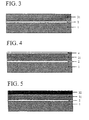
- Fig. 3
- eine Struktur bestehend aus dem Substrat, der Rückelektrode und der ersten ternären Phase PAS I;
- Fig. 4
- eine Struktur bestehend aus dem Substrat, der Rückelektrode, der ersten ternären Phase PAS I und einer Reaktionsschicht; und
- Fig. 5
- eine Struktur des Bauelements mit dem Substrat, der Rückelektrode und der polykristallinen Absorberschicht, bestehend aus den beiden ternären Phasen PAS I, PAS II.
- Die Solarzelle besteht aus einem Substrat 1, einer Rückelektrode 2, einer ersten ternären Phase (PAS I) 31 der polykristallinen Absorberschicht vom n-Leitungstyp, einer zweiten ternären Phase (PAS II) 32 der polykristallinen Absorberschicht, die an der Oberfläche vom p-Leitungstyp ist, so dass sich im Volumen der polykristallinen Absorberschicht die Potentialbarriere ausbildet, und einer transparenten Frontelektrode 5.
- Als Substrat 1 dient üblicherweise eine dünne, typischerweise 10 µm bis 30 µm dicke Stahifolie, die zusätzlich mit anderen Metallen oder Oxiden beschichtet sein kann. Andere Folien können ebenfalls eingesetzt werden.
- Auf dem Substrat 1 befindet sich eine 1 µm bis 5 µm dicke Rückelektrode 2 aus metallischen Phasen der Elemente Kupfer und Indium. Darüber ist die erste ternäre Phase 31 der polykristallinen Absorberschicht - aus der Phase CuIn5S8 bestehend - angeordnet. Diese stabile ternäre Phase 31 hat Spinellstruktur, ist vom n-Leitungstyp und besitzt bei Raumtemperatur eine für Solaranwendungen geeignete Bandlücke von 1,51 eV. Sie hat typischerweise eine Dicke von 0,5 µm bis 1 µm.
- Unmittelbar auf der PAS I 31 befindet sich die zweite ternäre Phase 32 der polykristallinen Absorberschicht, die aus CuInS2 besteht. Diese stabile ternäre Phase 32 hat Chalkopyritstruktur, kann durch Eigendotierung sowohl vom n-Leitungstyp als auch vom p-Leitungstyp sein und besitzt eine für Solaranwendungen geeignete Bandlücke.
- Die ternäre Phase PAS II 32 ist typischerweise zwischen 0,1 µm und 1 µm dick. Die PAS II 32 ist an der Oberfläche vom p-Leitungstyp, so dass sich im Volumen der polykristallinen Absorberschicht die Potentialbarriere zur Trennung der lichterzeugten Ladungsträger ausbildet. Auf der polykristallinen Absorberschicht ist die transparente Ableitelektrode 5 angeordnet. Diese besteht vorzugsweise aus CuJ vom p-Leitungstyp mit einem geringen spezifischen Widerstand. Die Dicke der CuJ-Schicht beträgt typischerweise 0,5 µm bis 2 µm.
- Eine weitere Möglichkeit ist die Anordnung einer transparenten Ableitelektrode 5 aus fremddotiertem ZnO vom n-Leitungstyp mit hoher spezifischer Leitfähigkeit auf der polykristallinen Absorberschicht mit Potentialbarriere. Diese Schicht hat typischerweise eine Dicke von 1 µm. Durch die quasi metallische Leitfähigkeit dieser TCO-Schicht bildet sich zwischen der polykristallinen Absorberschicht, die an der Grenzfläche zur Ableitelektrode vom p-Leitungstyp ist, und der Ableitelektrode vom n-Leitungstyp keine Potentialbarriere aus. In der Grenzfläche zwischen der dort p-leitenden polykristallinen Absorberschicht und dem TCO vom n-Leitungstyp entsteht eine Tunneldiode, die im Arbeitsbereich der Solarzelle eine ohmsche Charakteristik aufweist. Zwischen die polykristalline Absorberschicht mit Potentialbarriere und die Ableitelektrode vom n-Leitungstyp können dünne Bufferschichten vom p-Leitungstyp aus Cu2O, Cu(S, O) oder CuS mit geringem spezifischen Widerstand angeordnet sein. Sie sind typischerweise 20 nm bis 50 mn dick.
- Diese Bufferschichten dienen der Optimierung der Charakteristik der Tunneldiode zwischen der polykristallinen Absorberschicht mit Potentialbarriere und der hochleitfähigen Ableitelektrode.
- Auf die flexible Folie, die das Substrat 1 der Solarzelle bildet, werden nacheinander in einem Rolle-zu-Rolle Prozess die Metalle Kupfer (Cu) und Indium (In) vorzugsweise elektrolytisch abgeschieden.
- Dies ist ein sehr materialeffizientes und anlagentechnisch relativ einfaches Verfahren. Auch die Abscheidung der Metalle durch Sputter- und Vakuumverdampfungsprozesse oder Kombinationen dieser Prozesse sind möglich. Die Kupferschicht ist vorzugsweise 1 µm bis 5 µm dick, die Dicke der Indiumschicht beträgt typischerweise 0,5 µm bis 2 µm.
- Danach wird die mit dem Cu/In-Precursor beschichtete Folie in einem Rolle-zu-Rolle Prozesse in einem Schmalspaltreaktor im Sekundenbereich chalkogenisiert. Der Precursor wird vorzugsweise im Millisekundenbereich auf 450 °C bis 550 °C unter Inertgasatmosphäre erhitzt. Das Indium schmilzt dabei auf, Kupfer wird laut Phasendiagranun in die Schmelze eingelöst.
- Anschließend wird der Precursor in schwefelhaltigem Reaktionsgas, vorzugsweise in schwefelhaltigem Stickstoffträgergas chalkogenisiert. Die Chalkogenisierung dauert etwa 1 bis 3 Sekunden. Bei diesem Prozess wird eine typischerweise 1 µm bis 2 µm dicke CuIn5S8-Phase 31 gebildet. Diese stabile ternäre Phase 31 hat Spinellstruktur, ist n-leitend und besitzt bei Raumtemperatur eine für Solaranwendungen geeignete Bandlücke von 1,51 eV. Nach der Chalkogenisierung wird die Folie unter Inertgasatmosphäre im Sekundenbereich auf Raumtemperatur abgekühlt. Dabei erstarrt der Restprecursor unter Bildung von intermetallischen Cu/In-Phasen, vorzugsweise der Cu7In3-Phase, die die Rückelektrode 2 der Solarzelle bildet. Der gesamte Prozess "Aufheizung - Chalkogenisierung - Abkühlung" dauert typischerweise zwischen 3 s und 8 s.
- In einem nächsten Schritt wird vorzugsweise in einem Rolle-zu-Rolle Prozess eine typischerweise 50 nm bis 200 nm dicke Schicht aus Kupfersulfid 4 abgeschieden, indem das Band zunächst in einem sogenannten Spin-on-Verfahren. einem Walzenauftragsverfahren oder einem Rakelauftragsverfahren oberflächlich mit einer Lösung aus Thioharnstoff und Kupferacetat beschichtet und nachfolgend getrocknet und formiert wird. Danach wird die mit Kupfersulfid 4 beschichtete polykristalline Absorberschicht 31 in einem Rolle-zu-Rolle Prozess getempert. Die beschichtete Folie wird dazu vorzugsweise im Millisekundenbereich durch Wärmeleitung auf 550 °C bis 600 °C unter Inertgasatmosphäre erhitzt.
- Danach schließt sich ein Temperprozeß von 1 bis 10 s, vorzugsweise in Inertgasatmosphäre, an. Während dieses Temperprozesses reagieren die ternäre CuIn5S8-Phase und die binäre Kupfersulfid Phase teilweise miteinander zu einer ternären polykristallinen CuInS2-Phase 32, die an der Oberfläche p-leitend ist. Die an der Oberfläche p-leitende polykristalline Absorberschicht 32 ist typischerweise 100 nm bis 500 nm dick. Die gesamte polykristalline Absorberschicht besteht nach der Temperung aus einem heterogenen Gefüge der Phasen CuIn5S8 31 und CuInS2 32, die vertikal übereinander geschichtet sind, wobei die polykristalline Absorberschicht 31 vom n-Leitungstyp, die polykristalline Absorberschicht 32 an der Oberfläche vom p-Leitungstyp ist, und weist im Volumen eine Potentialbarriere zur Trennung der lichterzeugten Ladungsträger auf
- Nach der Temperung wird die Folie im Sekundenbereich unter Inertgasatmosphäre auf Raumtemperatur abgekühlt. Der gesamte Prozess "Aufheizen - Tempern - Abkühlen" dauert vorzugsweise 3 s bis 15 s. In einem nachfolgenden Schritt kann die noch verbliebene Kupfersulfldschicht 4 ätztechnisch entfernt werden.
- In einem letzten Schritt wird auf die polykristalline Absorberschicht 32 eine Frontelektrode 5 zur Abführung der Ladungsträger aufgebracht.
Claims (7)
- Dünnschichtsolarzelle auf der Basis von Ib/IIIa/VIa-Verbindungshalbleitern,
mit einem Substrat (1) aus einer flexiblen Folie,
einer Rückelektrode (2) aus Cu und In, welche sich auf dem Substrat (1) befindet,
mit einer photoaktiven polykristallinen Absorberschicht aus einem heterogenen Gefüge von zwei Ib/IIIa/VIa-Phasen (31, 32), die vertikal übereinander geschichtet sind,
wobei die erste Phase (31) der polykristallinen Absorberschicht über der Rückelektrode (2) angeordnet und aus der ternären Phase CuIn5S8 vom n-Leitungstyp gebildet ist und
die zweite Phase (32) der polykristallinen Absorberschicht sich unmittelbar auf der ersten Phase (31) befindet, aus der ternären Phase CuInS2 gebildet und an ihrer zur Licht einfallenden Seite weisenden Oberfläche vom p-Leitungstyp ist, so dass die Absorberschicht eine Potentialbarriere im Volumen aufweist. - Dünnschichtsolarzelle nach Anspruch 1, dadurch gekennzeichnet, dass sich auf der Oberfläche der Absorberschicht eine transparente Frontelektrode (5) befindet.
- Dünnschichtsolarzelle nach Anspruch 2, dadurch gekennzeichnet, dass die Frontelektrode (5) aus CuJ vom p-Leitungstyp besteht.
- Dünnschichtsolarzelle nach Anspruch 2, dadurch gekennzeichnet, dass die Frontelektrode (5) aus einer TCO-Schicht aus ZnO vom n-Leitungstyp mit hoher metallischer Leitfähigkeit besteht und dass in der Grenzfläche zwischen der dort p-leitenden Absorberschicht und der TCO-Schicht eine Tunnelelektrode ausgebildet ist.
- Dünnschichtsolarzelle nach Anspruch 4, dadurch gekennzeichnet, dass zwischen der Absorberschicht und der Frontelektrode (5) dünne Pufferschichten vom p-Leitungstyp aus Cu2O, Cu(S, O) oder CuS angeordnet sind.
- Verfahren zum Herstellen einer Dünnschichtsolarzelle nach einem der vorhergehenden Ansprüche, dadurch gekennzeichnet, dass- auf einem Substrat die Ib- und IIIa-Metalle Cu und In abgeschieden werden,- in einem Chalkogenisierungsprozess eine erste Ib/IIIa/VIa-Phase (31) aus CuIn5S8 vom n-Leitungstyp erzeugt wird,- auf der Oberfläche dieser Phase eine Ib/VIa-Phase aus Kupfersulfid abgeschieden wird,- in einem Temperprozess die erste Ib/IIIa/VIa-Phase mit der Ib/VIa-Phase teilweise zu einer zweiten Ib/IIIa/VIa-Phase (32) aus CuInS2 reagiert, die an ihrer Oberfläche vom p-Leitungstyp ist, so dass eine photoaktive polykristalline Absorberschicht eines heterogenen Gefüges von zwei Ib/IIIa/VIa-Phasen gebildet wird, die vertikal übereinander geschichtet sind und im Volumen die Potentialbarriere aufweisen.
- Verfahren nach Anspruch 10 oder 11, dadurch gekennzeichnet, dass die Ib/VIa-Phase Cu(2-x)S (0<x<1) ist.
Applications Claiming Priority (2)
| Application Number | Priority Date | Filing Date | Title |
|---|---|---|---|
| DE19921514A DE19921514A1 (de) | 1999-05-10 | 1999-05-10 | Dünnschichtsolarzelle auf der Basis der Ia/IIIb/VIa- Verbindungshalbleiter mit Potentialbarriere innerhalb der photoaktiven polykristallinen Absorberschicht und Verfahren zu ihrer Herstellung |
| DE19921514 | 1999-05-10 |
Publications (3)
| Publication Number | Publication Date |
|---|---|
| EP1052702A2 EP1052702A2 (de) | 2000-11-15 |
| EP1052702A3 EP1052702A3 (de) | 2007-03-07 |
| EP1052702B1 true EP1052702B1 (de) | 2010-11-24 |
Family
ID=7907591
Family Applications (1)
| Application Number | Title | Priority Date | Filing Date |
|---|---|---|---|
| EP00109198A Expired - Lifetime EP1052702B1 (de) | 1999-05-10 | 2000-05-09 | Dünnschichtsolarzelle auf der Basis der Ib/IIIa/VIa-Verbindungshalbleiter mit Potentialbarriere innerhalb der Absorberschicht und Verfahren zum Herstellen einer solchen Solarzelle |
Country Status (4)
| Country | Link |
|---|---|
| EP (1) | EP1052702B1 (de) |
| AT (1) | ATE489731T1 (de) |
| DE (2) | DE19921514A1 (de) |
| ES (1) | ES2357190T3 (de) |
Families Citing this family (3)
| Publication number | Priority date | Publication date | Assignee | Title |
|---|---|---|---|---|
| DE10350989A1 (de) * | 2003-10-30 | 2005-07-07 | Universität Leipzig | Dünnschichtsolarzelle |
| EP2159846A1 (de) | 2008-08-29 | 2010-03-03 | ODERSUN Aktiengesellschaft | Dünnfilmsolarzelle und photovoltaische Stranganordnung |
| DE102010015740B4 (de) | 2010-04-21 | 2013-04-11 | Mühlbauer Ag | Vorrichtung zur Herstellung eines Solarmoduls mit flexiblen Dünnschicht-Solarzellen |
Family Cites Families (4)
| Publication number | Priority date | Publication date | Assignee | Title |
|---|---|---|---|---|
| US4335266A (en) * | 1980-12-31 | 1982-06-15 | The Boeing Company | Methods for forming thin-film heterojunction solar cells from I-III-VI.sub.2 |
| EP0534459B1 (de) * | 1991-09-27 | 2000-07-26 | Matsushita Electric Industrial Co., Ltd. | Verfahren zur Herstellung einer Verbindungshalbleiter-Dünnschicht |
| US5436204A (en) * | 1993-04-12 | 1995-07-25 | Midwest Research Institute | Recrystallization method to selenization of thin-film Cu(In,Ga)Se2 for semiconductor device applications |
| JP3414814B2 (ja) * | 1994-01-24 | 2003-06-09 | 松下電器産業株式会社 | 太陽電池とその製造方法 |
-
1999
- 1999-05-10 DE DE19921514A patent/DE19921514A1/de not_active Ceased
-
2000
- 2000-05-09 DE DE50016036T patent/DE50016036D1/de not_active Expired - Lifetime
- 2000-05-09 ES ES00109198T patent/ES2357190T3/es not_active Expired - Lifetime
- 2000-05-09 AT AT00109198T patent/ATE489731T1/de active
- 2000-05-09 EP EP00109198A patent/EP1052702B1/de not_active Expired - Lifetime
Also Published As
| Publication number | Publication date |
|---|---|
| ATE489731T1 (de) | 2010-12-15 |
| DE19921514A1 (de) | 2000-11-30 |
| EP1052702A2 (de) | 2000-11-15 |
| DE50016036D1 (de) | 2011-01-05 |
| EP1052702A3 (de) | 2007-03-07 |
| ES2357190T3 (es) | 2011-04-19 |
Similar Documents
| Publication | Publication Date | Title |
|---|---|---|
| EP1052703B1 (de) | Dünnschichtsolarzelle auf der Basis der Ib/IIIa/VIa-Verbindungshalbleiter und Verfahren zum Herstellen einer solchen Solarzelle | |
| EP0715358B1 (de) | Verfahren zur Herstellung einer Solarzelle mit Chalkopyrit-Absorberschicht und so hergestellte Solarzelle | |
| EP0787354B1 (de) | Herstellungsverfahren von dünnschicht-solarzellen | |
| EP0219763B1 (de) | Solarzelle | |
| US8153889B2 (en) | Roll-to-roll integration of thin film solar modules | |
| DE102012100795B4 (de) | Superstrat-Solarzelle und Verfahren zu deren Herstellung | |
| DE102013104232B4 (de) | Solarzelle | |
| US8415559B2 (en) | Method for forming copper indium gallium chalcogenide layer with shaped gallium profile | |
| US20110048524A1 (en) | Thin film solar cell and method of manufacturing the same | |
| EP2758993B1 (de) | Dünnschichtsolarmodul mit serienverschaltung und verfahren zur serienverschaltung von dünnschichtsolarzellen | |
| EP2485266B2 (de) | Photoelektrische Umwandlungsvorrichtung und Verfahren zu deren Herstellung | |
| DE112008003755T5 (de) | Integrierte Struktur einer Solarzelle auf CIS-Grundlage | |
| DE112008003756T5 (de) | Stapelstruktur und integrierte Struktur einer Solarzelle auf CIS-Grundlage | |
| EP2590224B1 (de) | Photoelektrische umwandlungsvorrichtung | |
| EP2369631A2 (de) | Dünnfilm-Photovoltaikzelle | |
| EP2487724A2 (de) | Photovoltaische stromerzeugungsvorrichtung und verfahren zu ihrer herstellung | |
| DE102004049197A1 (de) | Solarbatterie und Herstellverfahren für eine solche | |
| DE102012109883A1 (de) | Verfahren zum Herstellen einer Dünnschichtsolarzelle mit pufferfreiem Fertigungsprozess | |
| CN112786737A (zh) | Cigs薄膜太阳能电池组件及其刻划方法 | |
| DE102012216026B4 (de) | Verfahren zur Herstellung einer flexiblen Photovoltaik-Dünnschichtzelle mit einer Eisendiffusionsbarriereschicht und flexible Photovoltaik-Dünnschichtzelle mit einer Eisendiffusionsbarriereschicht | |
| DE112009002356T5 (de) | Dünnschicht-Solarzellenreihe | |
| Kessler et al. | CIGS thin film photovoltaic—approaches and challenges | |
| EP1052702A2 (de) | Dünnschichtsolarzelle auf der Basis der Ib/IIIa/VIa-Verbindungshalbleiter mit Potentialbarriere innerhalb der Absorberschicht und Verfahren zum Herstellen einer solchen Solarzelle | |
| EP0798786B1 (de) | Solarzelle mit einer Chalkopyrit-Absorberschicht | |
| EP2704207A1 (de) | Photovoltaik-wechselrichter |
Legal Events
| Date | Code | Title | Description |
|---|---|---|---|
| PUAI | Public reference made under article 153(3) epc to a published international application that has entered the european phase |
Free format text: ORIGINAL CODE: 0009012 |
|
| AK | Designated contracting states |
Kind code of ref document: A2 Designated state(s): AT BE CH CY DE DK ES FI FR GB GR IE IT LI LU MC NL PT SE |
|
| AX | Request for extension of the european patent |
Free format text: AL;LT;LV;MK;RO;SI |
|
| PUAL | Search report despatched |
Free format text: ORIGINAL CODE: 0009013 |
|
| AK | Designated contracting states |
Kind code of ref document: A3 Designated state(s): AT BE CH CY DE DK ES FI FR GB GR IE IT LI LU MC NL PT SE |
|
| AX | Request for extension of the european patent |
Extension state: AL LT LV MK RO SI |
|
| RAP1 | Party data changed (applicant data changed or rights of an application transferred) |
Owner name: ODERSUN AKTIENGESELLSCHAFT |
|
| 17P | Request for examination filed |
Effective date: 20070831 |
|
| 17Q | First examination report despatched |
Effective date: 20071011 |
|
| AKX | Designation fees paid |
Designated state(s): AT BE CH CY DE DK ES FI FR GB GR IE IT LI LU MC NL PT SE |
|
| GRAP | Despatch of communication of intention to grant a patent |
Free format text: ORIGINAL CODE: EPIDOSNIGR1 |
|
| GRAS | Grant fee paid |
Free format text: ORIGINAL CODE: EPIDOSNIGR3 |
|
| GRAA | (expected) grant |
Free format text: ORIGINAL CODE: 0009210 |
|
| AK | Designated contracting states |
Kind code of ref document: B1 Designated state(s): AT BE CH CY DE DK ES FI FR GB GR IE IT LI LU MC NL PT SE |
|
| REG | Reference to a national code |
Ref country code: GB Ref legal event code: FG4D Free format text: NOT ENGLISH |
|
| REG | Reference to a national code |
Ref country code: CH Ref legal event code: EP |
|
| REG | Reference to a national code |
Ref country code: IE Ref legal event code: FG4D |
|
| REF | Corresponds to: |
Ref document number: 50016036 Country of ref document: DE Date of ref document: 20110105 Kind code of ref document: P |
|
| REG | Reference to a national code |
Ref country code: NL Ref legal event code: VDEP Effective date: 20101124 |
|
| REG | Reference to a national code |
Ref country code: GR Ref legal event code: EP Ref document number: 20110400468 Country of ref document: GR Effective date: 20110317 |
|
| REG | Reference to a national code |
Ref country code: ES Ref legal event code: FG2A Ref document number: 2357190 Country of ref document: ES Kind code of ref document: T3 Effective date: 20110419 |
|
| PG25 | Lapsed in a contracting state [announced via postgrant information from national office to epo] |
Ref country code: FI Free format text: LAPSE BECAUSE OF FAILURE TO SUBMIT A TRANSLATION OF THE DESCRIPTION OR TO PAY THE FEE WITHIN THE PRESCRIBED TIME-LIMIT Effective date: 20101124 Ref country code: SE Free format text: LAPSE BECAUSE OF FAILURE TO SUBMIT A TRANSLATION OF THE DESCRIPTION OR TO PAY THE FEE WITHIN THE PRESCRIBED TIME-LIMIT Effective date: 20101124 Ref country code: CY Free format text: LAPSE BECAUSE OF FAILURE TO SUBMIT A TRANSLATION OF THE DESCRIPTION OR TO PAY THE FEE WITHIN THE PRESCRIBED TIME-LIMIT Effective date: 20101124 Ref country code: PT Free format text: LAPSE BECAUSE OF FAILURE TO SUBMIT A TRANSLATION OF THE DESCRIPTION OR TO PAY THE FEE WITHIN THE PRESCRIBED TIME-LIMIT Effective date: 20110324 Ref country code: NL Free format text: LAPSE BECAUSE OF FAILURE TO SUBMIT A TRANSLATION OF THE DESCRIPTION OR TO PAY THE FEE WITHIN THE PRESCRIBED TIME-LIMIT Effective date: 20101124 |
|
| REG | Reference to a national code |
Ref country code: IE Ref legal event code: FD4D |
|
| PG25 | Lapsed in a contracting state [announced via postgrant information from national office to epo] |
Ref country code: IE Free format text: LAPSE BECAUSE OF FAILURE TO SUBMIT A TRANSLATION OF THE DESCRIPTION OR TO PAY THE FEE WITHIN THE PRESCRIBED TIME-LIMIT Effective date: 20101124 |
|
| PGFP | Annual fee paid to national office [announced via postgrant information from national office to epo] |
Ref country code: ES Payment date: 20110526 Year of fee payment: 12 Ref country code: FR Payment date: 20110607 Year of fee payment: 12 Ref country code: GR Payment date: 20110527 Year of fee payment: 12 |
|
| PG25 | Lapsed in a contracting state [announced via postgrant information from national office to epo] |
Ref country code: DK Free format text: LAPSE BECAUSE OF FAILURE TO SUBMIT A TRANSLATION OF THE DESCRIPTION OR TO PAY THE FEE WITHIN THE PRESCRIBED TIME-LIMIT Effective date: 20101124 |
|
| PGFP | Annual fee paid to national office [announced via postgrant information from national office to epo] |
Ref country code: GB Payment date: 20110525 Year of fee payment: 12 |
|
| PGFP | Annual fee paid to national office [announced via postgrant information from national office to epo] |
Ref country code: IT Payment date: 20110525 Year of fee payment: 12 |
|
| PLBE | No opposition filed within time limit |
Free format text: ORIGINAL CODE: 0009261 |
|
| STAA | Information on the status of an ep patent application or granted ep patent |
Free format text: STATUS: NO OPPOSITION FILED WITHIN TIME LIMIT |
|
| 26N | No opposition filed |
Effective date: 20110825 |
|
| BERE | Be: lapsed |
Owner name: ODERSUN A.G. Effective date: 20110531 |
|
| PGFP | Annual fee paid to national office [announced via postgrant information from national office to epo] |
Ref country code: DE Payment date: 20110729 Year of fee payment: 12 |
|
| REG | Reference to a national code |
Ref country code: DE Ref legal event code: R097 Ref document number: 50016036 Country of ref document: DE Effective date: 20110825 |
|
| PG25 | Lapsed in a contracting state [announced via postgrant information from national office to epo] |
Ref country code: MC Free format text: LAPSE BECAUSE OF NON-PAYMENT OF DUE FEES Effective date: 20110531 |
|
| REG | Reference to a national code |
Ref country code: CH Ref legal event code: PL |
|
| PG25 | Lapsed in a contracting state [announced via postgrant information from national office to epo] |
Ref country code: LI Free format text: LAPSE BECAUSE OF NON-PAYMENT OF DUE FEES Effective date: 20110531 Ref country code: CH Free format text: LAPSE BECAUSE OF NON-PAYMENT OF DUE FEES Effective date: 20110531 |
|
| PG25 | Lapsed in a contracting state [announced via postgrant information from national office to epo] |
Ref country code: BE Free format text: LAPSE BECAUSE OF NON-PAYMENT OF DUE FEES Effective date: 20110531 |
|
| REG | Reference to a national code |
Ref country code: AT Ref legal event code: MM01 Ref document number: 489731 Country of ref document: AT Kind code of ref document: T Effective date: 20110509 |
|
| GBPC | Gb: european patent ceased through non-payment of renewal fee |
Effective date: 20120509 |
|
| PG25 | Lapsed in a contracting state [announced via postgrant information from national office to epo] |
Ref country code: AT Free format text: LAPSE BECAUSE OF NON-PAYMENT OF DUE FEES Effective date: 20110509 |
|
| REG | Reference to a national code |
Ref country code: GR Ref legal event code: ML Ref document number: 20110400468 Country of ref document: GR Effective date: 20121204 |
|
| PG25 | Lapsed in a contracting state [announced via postgrant information from national office to epo] |
Ref country code: GR Free format text: LAPSE BECAUSE OF NON-PAYMENT OF DUE FEES Effective date: 20121204 Ref country code: IT Free format text: LAPSE BECAUSE OF NON-PAYMENT OF DUE FEES Effective date: 20120509 |
|
| REG | Reference to a national code |
Ref country code: FR Ref legal event code: ST Effective date: 20130131 |
|
| REG | Reference to a national code |
Ref country code: DE Ref legal event code: R119 Ref document number: 50016036 Country of ref document: DE Effective date: 20121201 |
|
| PG25 | Lapsed in a contracting state [announced via postgrant information from national office to epo] |
Ref country code: FR Free format text: LAPSE BECAUSE OF NON-PAYMENT OF DUE FEES Effective date: 20120531 Ref country code: GB Free format text: LAPSE BECAUSE OF NON-PAYMENT OF DUE FEES Effective date: 20120509 |
|
| PG25 | Lapsed in a contracting state [announced via postgrant information from national office to epo] |
Ref country code: LU Free format text: LAPSE BECAUSE OF NON-PAYMENT OF DUE FEES Effective date: 20110509 |
|
| PG25 | Lapsed in a contracting state [announced via postgrant information from national office to epo] |
Ref country code: DE Free format text: LAPSE BECAUSE OF NON-PAYMENT OF DUE FEES Effective date: 20121201 |
|
| REG | Reference to a national code |
Ref country code: ES Ref legal event code: FD2A Effective date: 20131030 |
|
| PG25 | Lapsed in a contracting state [announced via postgrant information from national office to epo] |
Ref country code: ES Free format text: LAPSE BECAUSE OF NON-PAYMENT OF DUE FEES Effective date: 20120510 |