EP1052563A2 - Synchronous signal processing system - Google Patents
Synchronous signal processing system Download PDFInfo
- Publication number
- EP1052563A2 EP1052563A2 EP00109909A EP00109909A EP1052563A2 EP 1052563 A2 EP1052563 A2 EP 1052563A2 EP 00109909 A EP00109909 A EP 00109909A EP 00109909 A EP00109909 A EP 00109909A EP 1052563 A2 EP1052563 A2 EP 1052563A2
- Authority
- EP
- European Patent Office
- Prior art keywords
- clock signal
- signal
- signal processing
- circuit
- clock
- Prior art date
- Legal status (The legal status is an assumption and is not a legal conclusion. Google has not performed a legal analysis and makes no representation as to the accuracy of the status listed.)
- Withdrawn
Links
Images




Classifications
-
- H—ELECTRICITY
- H03—ELECTRONIC CIRCUITRY
- H03L—AUTOMATIC CONTROL, STARTING, SYNCHRONISATION OR STABILISATION OF GENERATORS OF ELECTRONIC OSCILLATIONS OR PULSES
- H03L7/00—Automatic control of frequency or phase; Synchronisation
- H03L7/06—Automatic control of frequency or phase; Synchronisation using a reference signal applied to a frequency- or phase-locked loop
-
- G—PHYSICS
- G06—COMPUTING OR CALCULATING; COUNTING
- G06F—ELECTRIC DIGITAL DATA PROCESSING
- G06F1/00—Details not covered by groups G06F3/00 - G06F13/00 and G06F21/00
- G06F1/04—Generating or distributing clock signals or signals derived directly therefrom
- G06F1/10—Distribution of clock signals, e.g. skew
Definitions
- the present invention relates to a synchronous signal processing system and, more particularly, to a technique for handling a signal processing system having a plurality of processors operating with different clock signals as a synchronous circuit operating with a single clock signal.
- a signal processing system including a plurality of processors operating with different clock signals be handled as a synchronous system operating with a single system clock signal.
- Fig. 1 shows a timing chart of signals in a typical video signal processor, implemented as a video signal sampling circuit.
- the video signal sampling circuit samples a video signal based on a system clock signal.
- the sampled video signal is then supplied to a succeeding stage circuit together with the system clock signal for allowing the succeeding stage circuit to process the sampled video signal.
- the signal processing system including the sampling circuit and succeeding signal processing circuits for processing the output of the sampling circuit can be designed as a synchronous system operating with the single system clock signal.
- a CPU used in a signal processing system has a phase difference between the input clock signal and the output clock signal thereof, wherein the phase difference therebetween is not defined.
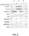
- Fig. 2 shows another timing chart of signals used in a signal processing system including a CPU. In the signal processing system, the timings of the signals are defined based on the output clock signal supplied from the CPU. Thus, if a plurality of CPUs or processors are disposed in a single system, the design for synchronization is difficult in the system.
- Patent Publication JP-A-11-41095 describes a technique for adjusting the phase in a PLL circuit, which is thus indispensable to the system, as recited in the publication.
- Patent Publication JP-A-5-324868 describes another technique for adjustment of phases between the input clock signal and the output clock signal of a CPU.
- the signal processing system includes a data path circuit (processor) 11, a CPU 12, a system clock generator 17 for delivering a system clock signal f1, a PLL circuit for generating a first clock signal f3 in synchrony with the system clock signal f1 based on the system clock signal f1, a set of external interfaces 16, and a user data logic (UDL) block 14 for receiving/transmitting data using an internal bus.
- the CPU 12 receives the first clock signal f3 and delivers data together with a second clock signal f2 generated in the CPU 12.
- the UDL block 14 includes a first UDL circuit 15A, a second UDL circuit 15B and a clock exchanger 18, and receives and transmits data from/to the external interface 16, the data path circuit 11 and the CPU 12 by using the first and second UDL circuits 15A and 15B.
- the first UDL circuit 15A receives/transmits data to the data path circuit 11 based on the first clock signal f3, whereas the second UDL circuit 15B receives/transmits data to the CPU 12 and external interface 16 based on the second clock signal f2, the first and second clock signals f3 and f2 being exchanged by the clock exchanger 18.
- the data path circuit 11 uses the first clock signal f3 supplied from the PLL circuit 13.
- the clock exchanger 18 receives the first and second clock signals f3 and f2 at terminals Ick1 and Ick2, and functions for exchanging the first and second clock signals Ick1 and Ixc2 for the UDL circuits 15A and 15B, whereby signal transmission of the data between the data path circuit 11 and the external interface 16 is operated on the first clock signal f3 and signal transmission of the data between the CPU 12 and the external circuit is operated on the second clock signal f2.
- the data path circuit 11 operates with the first clock signal f3 for data processing therein.
- the present invention provides a signal processing system including a first processing unit for signal processing based on a system clock signal, a PLL circuit for generating a first clock signal based on the system clock signal, a second processing unit for generating a second clock signal based on the first clock signal and signal processing based on the second clock signal, wherein the PLL circuit receives the second clock signal as a feed-back signal to deliver the first clock signal so that a phase difference between the system clock signal and the second clock signal assumes zero.
- the signal processing system including the first and second processing units can be handled as a synchronous circuit which operates with the single system clock signal, without using a clock exchanger.
- a signal processing system includes a data path circuit 11 as a first processor, a CPU (CPU core) 12 as a second processor, a system clock generator 17 for delivering a system clock signal f1, a PLL circuit 13 for generating a first clock signal f3 based on the system clock signal f1, a set of external interfaces 16, a UDL block 14 as a third processor for receiving/transmitting data, and data buses 21 to 25 for data transmission.
- the UDL block 14 includes first UDL circuit 15A and a second UDL circuit 15B, and operates for data transmission between the data path circuit 11 or the CPU 12 and the external interface 16 through the data bus by using the first and second UDL circuits 15A and 15B.
- the first and second UDL circuits 15A and 15B operate with the second clock signal f2 received at the clock inputs Ick of the UDL circuits 15A and 15B.
- the data path circuit 11 operates with the system clock signal f1 supplied from the system clock generator 17.
- the system clock generator 17 delivers the system clock signal f1 to the PLL circuit 13 at the clock input Ir thereof, and to the data path circuit 11 at the clock input Ick thereof.
- the PLL circuit 13 generates the first clock signal f3 and delivers the same to the CPU 12.
- the CPU 12 receives the first clock signal f3 and delivers data together with a second clock signal f2 generated in the CPU 12 based on the first clock signal f3.
- the PLL circuit 13 receives the system cock signal f1 at the clock input Ir thereof, and also the second clock signal f2 at the feed-back input Ic thereof.
- the PLL circuit 13 oscillates at a frequency same as the frequency of the system clock signal f1 to deliver, through the output Ock thereof, the second clock signal f2 which is controlled for skew adjustment with the system clock signal f1.
- the skew adjustment between the system clock signal f1 and the second clock signal f2 allows the UDL block 14 to operate with the second clock signal f2 in synchrony with the system clock signal f1.
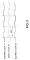
- the skew adjustment in the present embodiment will be described with reference to Fig. 5.
- N 1 in this example
- the phase of the second clock signal f2 coincides with the phase of the system clock signal f1, as shown in Fig. 5, while allowing the phase of the first clock signal f3 to be deviated significantly from the phases of the system clock signal f1 and the second clock signal f2.
- the signal processing system can be handled as a synchronous system while assuming that the system operates with the single system clock signal f1.
- a signal processing system is similar to the first embodiment except that an additional combination of a PLL circuit 13B and a CPU 12B is provided in the system and that the UDL block 14 includes three UDL circuits 15A, 15B and 15C each corresponding to one of data path circuit 11, CPU 12A and CPU 12B.
- the PLL circuit 13A, CPU 12A and UDL circuits 15A and 15B constitute a second processor block 18, and the PLL circuit 13B, CPU 12B and UDL circuit 15C constitute a third processor block 19, with the data path circuit 11 being the first processor block.
- Both the CPUs 12A and 12B operate with respective second clock signals f2 A and f2 B , the second clock signal f2 A having a frequency which is same as the frequency of the system clock signal f1, the second clock signal f2 B having a frequency which is double the frequency of the system clock signal f1.
- the phases of both the second clock signals f2 A and f2 B coincide with the phase of the system clock signal f1 due to the feed-back of the second clock signals f2 A and f2 B to the respective PLL circuits 13A and 13B for phase adjustment.
- the signal processing system including a plurality of CPUs 12A and 12B operating with different clock signals f2 A and f2 B having different frequencies can be handled as a synchronous circuit which operates with the system clock signal f1.
Landscapes
- Engineering & Computer Science (AREA)
- Theoretical Computer Science (AREA)
- Physics & Mathematics (AREA)
- General Engineering & Computer Science (AREA)
- General Physics & Mathematics (AREA)
- Synchronisation In Digital Transmission Systems (AREA)
- Synchronizing For Television (AREA)
- Picture Signal Circuits (AREA)
- Stabilization Of Oscillater, Synchronisation, Frequency Synthesizers (AREA)
Abstract
Description
Claims (7)
- A signal processing system comprising a first processing unit (11) for signal processing based on a system clock signal, a PLL circuit (13, 13A) for generating a first clock signal based on the system clock signal, a second processing unit (12, 12A) for generating a second clock signal based on the first clock signal and signal processing based on the second clock signal, characterized in that:the PLL circuit (13, 13A) receives the second clock signal as a feed-back signal to deliver the first clock signal so that a phase difference between the system clock signal and the second clock signal assumes zero.
- The signal processing system as defined in claim 1, further comprising a third processing unit (14) for operating with the second clock signal to receive/transmit data between the same and the second signal processing unit (12).
- The signal processing system as defined in claim 2, wherein the first signal processing unit is a video signal sampling circuit and the second processing unit is a CPU.
- The signal processing system as defined in claim 1, further comprising another PLL circuit (13B) for generating a third clock signal based on the system clock signal and a third signal processing unit (12B) generating a fourth clock signal based on the third clock signal and operating with the fourth clock signal, the another PLL circuit (13B) receiving the fourth clock signal as a feed-back signal to deliver the third clock signal so that a phase difference between the system clock signal and the fourth clock signal assumes zero.
- The signal processing system as defined in claim 4, further comprising a fourth signal processing unit (15C) for operating with the fourth clock signal to receive/transmit data between the same and the third signal processing unit.
- The signal processing unit as defined in claim 1, wherein the first clock signal and the second clock signal have a significant phase difference therebetween.
- The signal processing unit as defined in claim 1, wherein the first clock signal has a frequency obtained by multiplying the frequency of the system clock signal.
Applications Claiming Priority (2)
| Application Number | Priority Date | Filing Date | Title |
|---|---|---|---|
| JP13400499 | 1999-05-14 | ||
| JP13400499A JP3349983B2 (en) | 1999-05-14 | 1999-05-14 | Semiconductor integrated circuit device |
Publications (2)
| Publication Number | Publication Date |
|---|---|
| EP1052563A2 true EP1052563A2 (en) | 2000-11-15 |
| EP1052563A3 EP1052563A3 (en) | 2008-03-19 |
Family
ID=15118139
Family Applications (1)
| Application Number | Title | Priority Date | Filing Date |
|---|---|---|---|
| EP00109909A Withdrawn EP1052563A3 (en) | 1999-05-14 | 2000-05-10 | Synchronous signal processing system |
Country Status (3)
| Country | Link |
|---|---|
| US (1) | US6763080B1 (en) |
| EP (1) | EP1052563A3 (en) |
| JP (1) | JP3349983B2 (en) |
Families Citing this family (2)
| Publication number | Priority date | Publication date | Assignee | Title |
|---|---|---|---|---|
| US7483173B2 (en) | 2005-03-10 | 2009-01-27 | Kabushiki Kaisha Toshiba | Data processor having a synchronizing function of a plurality of chips |
| JP2008233304A (en) | 2007-03-19 | 2008-10-02 | Mitsubishi Electric Corp | Image data processing device |
Family Cites Families (16)
| Publication number | Priority date | Publication date | Assignee | Title |
|---|---|---|---|---|
| JPH02217919A (en) | 1989-02-17 | 1990-08-30 | Fujitsu Ltd | Elastic storage circuit |
| JPH02226824A (en) | 1989-02-28 | 1990-09-10 | Fujitsu Ltd | Phase adjusting circuit |
| JP2719226B2 (en) | 1990-10-01 | 1998-02-25 | 株式会社日立製作所 | Information processing system |
| JPH04225408A (en) | 1990-12-27 | 1992-08-14 | Konica Corp | Information processor |
| JP2770656B2 (en) | 1992-05-11 | 1998-07-02 | ヤマハ株式会社 | Integrated circuit device |
| US5355037A (en) | 1992-06-15 | 1994-10-11 | Texas Instruments Incorporated | High performance digital phase locked loop |
| JPH07281783A (en) | 1994-04-04 | 1995-10-27 | Mitsubishi Electric Corp | Semiconductor integrated circuit device |
| JP3368516B2 (en) | 1995-02-23 | 2003-01-20 | 富士通株式会社 | Repeater for New Synchronous Digital Hierarchy |
| JP2735097B2 (en) | 1995-07-20 | 1998-04-02 | 日本電気株式会社 | Semiconductor integrated circuit |
| US5565816A (en) * | 1995-08-18 | 1996-10-15 | International Business Machines Corporation | Clock distribution network |
| JPH09282042A (en) | 1996-04-15 | 1997-10-31 | Sony Corp | Data processing device |
| TW320701B (en) * | 1996-05-16 | 1997-11-21 | Resilience Corp | |
| US6141769A (en) * | 1996-05-16 | 2000-10-31 | Resilience Corporation | Triple modular redundant computer system and associated method |
| JPH10313349A (en) | 1997-05-13 | 1998-11-24 | Fujitsu Ltd | Data communication device |
| JP4033962B2 (en) | 1997-05-23 | 2008-01-16 | 株式会社ルネサステクノロジ | Clock generation circuit |
| JPH10324868A (en) | 1997-05-27 | 1998-12-08 | Mitsubishi Chem Corp | Thermal storage material composition |
-
1999
- 1999-05-14 JP JP13400499A patent/JP3349983B2/en not_active Expired - Fee Related
-
2000
- 2000-05-05 US US09/565,490 patent/US6763080B1/en not_active Expired - Lifetime
- 2000-05-10 EP EP00109909A patent/EP1052563A3/en not_active Withdrawn
Also Published As
| Publication number | Publication date |
|---|---|
| JP2000322150A (en) | 2000-11-24 |
| US6763080B1 (en) | 2004-07-13 |
| EP1052563A3 (en) | 2008-03-19 |
| JP3349983B2 (en) | 2002-11-25 |
Similar Documents
| Publication | Publication Date | Title |
|---|---|---|
| US5708801A (en) | Apparatus and method for operating chips synchronously at speeds exceeding the bus speed | |
| KR20030064379A (en) | System and method for synchronizing a skip pattern and initializing a clock forwarding interface in a multiple-clock system | |
| US5006979A (en) | Phase synchronization system | |
| US20100322365A1 (en) | System and method for synchronizing multi-clock domains | |
| JP3457459B2 (en) | Method for synchronizing data sent at external clock frequency with internal clock frequency and multiple clock converter | |
| US5335337A (en) | Programmable data transfer timing | |
| JPH10154021A (en) | Clock switching device and clock switching method | |
| US6425088B1 (en) | Method of the apparatus for transferring data between circuits | |
| US6763080B1 (en) | Synchronous signal processing system | |
| US8254513B2 (en) | Inter-device adaptable interfacing clock skewing | |
| JPH11205293A (en) | Internal clock synchronization method and internal clock synchronization circuit | |
| US6775339B1 (en) | Circuit design for high-speed digital communication | |
| US6810486B2 (en) | Method and apparatus for de-skewing a clock using a first and second phase locked loop and a clock tree | |
| US7123674B2 (en) | Reducing latency and power in asynchronous data transfers | |
| US7127632B2 (en) | Method and device for synchronizing integrated circuits | |
| US6430697B1 (en) | Method and apparatus for reducing data return latency of a source synchronous data bus by detecting a late strobe and enabling a bypass path | |
| JP3604637B2 (en) | Asynchronous transfer device and asynchronous transfer method | |
| JPH1115783A (en) | Synchronous circuit | |
| JP3039441B2 (en) | Synchronous edge detection method between different clocks and synchronous edge detection method between different clocks | |
| JP3709355B2 (en) | Clock synchronization system and method | |
| JPH117349A (en) | Electronic circuit and integrated circuit for noise reduction of bus wiring | |
| JP2002108809A (en) | Method and device for transferring source synchronous data | |
| US20040057548A1 (en) | Quasi-synchronous multi-stage event synchronization apparatus | |
| JPH02277331A (en) | Repeater | |
| JPH09274571A (en) | Interruption delay device |
Legal Events
| Date | Code | Title | Description |
|---|---|---|---|
| PUAI | Public reference made under article 153(3) epc to a published international application that has entered the european phase |
Free format text: ORIGINAL CODE: 0009012 |
|
| AK | Designated contracting states |
Kind code of ref document: A2 Designated state(s): AT BE CH CY DE DK ES FI FR GB GR IE IT LI LU MC NL PT SE |
|
| AX | Request for extension of the european patent |
Free format text: AL;LT;LV;MK;RO;SI |
|
| RAP1 | Party data changed (applicant data changed or rights of an application transferred) |
Owner name: NEC ELECTRONICS CORPORATION |
|
| PUAL | Search report despatched |
Free format text: ORIGINAL CODE: 0009013 |
|
| AK | Designated contracting states |
Kind code of ref document: A3 Designated state(s): AT BE CH CY DE DK ES FI FR GB GR IE IT LI LU MC NL PT SE |
|
| AX | Request for extension of the european patent |
Extension state: AL LT LV MK RO SI |
|
| PUAF | Information related to the publication of a search report (a3 document) modified or deleted |
Free format text: ORIGINAL CODE: 0009199SEPU |
|
| PUAL | Search report despatched |
Free format text: ORIGINAL CODE: 0009013 |
|
| D17D | Deferred search report published (deleted) | ||
| 17P | Request for examination filed |
Effective date: 20080201 |
|
| AK | Designated contracting states |
Kind code of ref document: A3 Designated state(s): AT BE CH CY DE DK ES FI FR GB GR IE IT LI LU MC NL PT SE |
|
| AX | Request for extension of the european patent |
Extension state: AL LT LV MK RO SI |
|
| 17Q | First examination report despatched |
Effective date: 20080609 |
|
| AKX | Designation fees paid |
Designated state(s): DE FR GB IT NL |
|
| RAP1 | Party data changed (applicant data changed or rights of an application transferred) |
Owner name: RENESAS ELECTRONICS CORPORATION |
|
| STAA | Information on the status of an ep patent application or granted ep patent |
Free format text: STATUS: THE APPLICATION HAS BEEN WITHDRAWN |
|
| 18W | Application withdrawn |
Effective date: 20140310 |