EP1052102A1 - Thermal printing head and protective cover used for the same - Google Patents
Thermal printing head and protective cover used for the same Download PDFInfo
- Publication number
- EP1052102A1 EP1052102A1 EP99901905A EP99901905A EP1052102A1 EP 1052102 A1 EP1052102 A1 EP 1052102A1 EP 99901905 A EP99901905 A EP 99901905A EP 99901905 A EP99901905 A EP 99901905A EP 1052102 A1 EP1052102 A1 EP 1052102A1
- Authority
- EP
- European Patent Office
- Prior art keywords
- protective cover
- main body
- circuit board
- heat sink
- engagement
- Prior art date
- Legal status (The legal status is an assumption and is not a legal conclusion. Google has not performed a legal analysis and makes no representation as to the accuracy of the status listed.)
- Granted
Links
Images




Classifications
-
- B—PERFORMING OPERATIONS; TRANSPORTING
- B41—PRINTING; LINING MACHINES; TYPEWRITERS; STAMPS
- B41J—TYPEWRITERS; SELECTIVE PRINTING MECHANISMS, i.e. MECHANISMS PRINTING OTHERWISE THAN FROM A FORME; CORRECTION OF TYPOGRAPHICAL ERRORS
- B41J2/00—Typewriters or selective printing mechanisms characterised by the printing or marking process for which they are designed
- B41J2/315—Typewriters or selective printing mechanisms characterised by the printing or marking process for which they are designed characterised by selective application of heat to a heat sensitive printing or impression-transfer material
- B41J2/32—Typewriters or selective printing mechanisms characterised by the printing or marking process for which they are designed characterised by selective application of heat to a heat sensitive printing or impression-transfer material using thermal heads
- B41J2/335—Structure of thermal heads
-
- B—PERFORMING OPERATIONS; TRANSPORTING
- B41—PRINTING; LINING MACHINES; TYPEWRITERS; STAMPS
- B41J—TYPEWRITERS; SELECTIVE PRINTING MECHANISMS, i.e. MECHANISMS PRINTING OTHERWISE THAN FROM A FORME; CORRECTION OF TYPOGRAPHICAL ERRORS
- B41J2/00—Typewriters or selective printing mechanisms characterised by the printing or marking process for which they are designed
- B41J2/315—Typewriters or selective printing mechanisms characterised by the printing or marking process for which they are designed characterised by selective application of heat to a heat sensitive printing or impression-transfer material
- B41J2/32—Typewriters or selective printing mechanisms characterised by the printing or marking process for which they are designed characterised by selective application of heat to a heat sensitive printing or impression-transfer material using thermal heads
- B41J2/345—Typewriters or selective printing mechanisms characterised by the printing or marking process for which they are designed characterised by selective application of heat to a heat sensitive printing or impression-transfer material using thermal heads characterised by the arrangement of resistors or conductors
Definitions
- the present invention relates to a thermal printhead for use in a facsimile or a printer as a printing means for example. It also relates to a protective cover for protecting drive ICs and wiring patterns or the like provided on the thermal printhead.
- a prior-art thermal printhead is disclosed for example in JP-A-8-258309.
- the disclosed thermal printhead includes a heat sink plate, a head substrate, and a circuit board.
- the head substrate and the circuit board are bonded to the heat sink plate with an adhesive.
- the head substrate has an upper surface on which a heating resistor and a plurality of drive ICs are mounted.
- the circuit board carries a connector for external connection and has an upper surface provided with a wiring pattern for connecting the drive ICs to the connector.
- the thermal printhead further includes a protective cover formed of a synthetic resin.
- the protective cover is so provided as to cover the wiring pattern on the circuit board and the drive ICs on the head substrate.
- the protective cover has a lower surface which is integrally formed with a plurality of engagement pawls. By flexing the protective cover widthwise appropriately, the engagement pawls are brought into engagement with the circuit board and the head substrate, thereby mounting the protective cover onto the thermal printhead. Conversely, the protective cover may be removed from the thermal printhead by disengaging the engagement pawls from the circuit board and the head substrate.
- the prior art thermal printhead has the following problems. As described above, since the protective cover mounted onto the circuit board and the head substrate is flexed, it tends to restore to its natural state, exerting a force on the circuit board and the head substrate to separate them from the heat sink plate. As a result, the circuit board and the head substrate may be partially lifted from the heat sink plate.
- the protective cover in such a flexed state onto the thermal printhead may cause another problem.
- a printing paper and/or an ink ribbon is pressed against the heating resistor on the head substrate by a platen roller.
- the protective cover which is undesirably flexed widthwise comes into contact with the printing paper and/or the ink ribbon strongly at a particular portion or portions.
- the printing paper and/or the ink ribbon may be broken or wrinkled.
- Another object of the present invention is to provide a protective cover which can be advantageously used in such a thermal printhead.
- a protective cover for use with a thermal printhead including a heat sink plate formed with a plurality of fixing holes, a head substrate, and a circuit board, the protective cover comprising: a main body having an obverse surface and a reverse surface; and a plurality of pins extending from the reverse surface; wherein each of the pins is designed for press-fitting into a respective one of the fixing holes.
- the protective cover is carried on the heat sink plate. Accordingly, it is possible to prevent the head substrate and the circuit board from being separated from the heat sink plate.
- the pins may be integrally formed on the main body. Alternatively, the pins may be formed separately from the main body and then bonded to the main body.
- each of the pins maybe formed with at least one slit facilitating press-fitting of the pin into a respective one of the fixing holes.
- the protective cover further includes a plurality of engagement pawls for engaging the head substrate, and each of the engagement pawls is integrally formed on the main body.
- Each of the engagement pawls may extend in the same direction as the pins.
- the protective cover may further include a plurality of protrusions projecting from the reverse surface of the main body, and each of the protrusions is provided adjacent to one of the engagement pawls.
- a thermal printhead comprising: a heat sink plate formed with a plurality of fixing holes; a head substrate carried on the heat sink plate and provided with a heating resistor and a plurality of drive ICs; a circuit board carried on the heat sink plate and formed with a predetermined wiring pattern; and a protective cover for covering the circuit board, the protective cover having a main body including an obverse surface and a reverse surface; wherein the protective cover has a plurality of pins extending from the reverse surface of the main body, each of the pins being designed for press-fitting into a respective one of the plurality of fixing holes in the heat sink plate.
- a protective cover for use with a thermal printhead including a heat sink plate, a head substrate, and a circuit board, the protective cover comprising an elongated main body including an obverse surface and a reverse surface, wherein the main body is warped so that a longitudinally central portion of the main body is located higher than other portions of the main body.
- the protective cover may further include a plurality of first engagement pieces protruding from the reverse surface of the main body for engagement with the circuit board.
- the protective cover may further include a plurality of protrusions protruding from the reverse surface of the main body for engagement with the heat sink plate.
- the protective cover may further include a plurality of second engagement pieces protruding from the reverse surface of the main body for engagement with the head substrate.
- the protrusions may be integrally formed on the main body.
- a thermal printhead comprising: a heat sink plate; a head substrate carried on the heat sink plate and provided with a heating resistor and a plurality of drive ICs; a circuit board carried on the heat sink plate and formed with a predetermined wiring pattern; and a protective cover for covering the circuit board, the protective cover having an elongated main body including an obverse surface and a reverse surface; wherein the main body is warped so that a longitudinally central portion of the main body is located higher than other portions of the main body.
- the protective cover is provided with a plurality of protrusions for engagement with the heat sink plate.
- the circuit board is formed with a plurality of through-holes for allowing passage of the protrusions.
- the protective cover may be provided with a plurality of first engagement pieces protruding from the reverse surface of the main body for engagement with the circuit board.
- the circuit board may include cutouts for engagement with the first engagement pieces.
- the protective cover may be provided with a plurality of second engagement pieces protruding from the reverse surface of the main body for engagement with the head substrate.
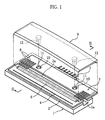
- Fig. 1 schematically shows a thermal printhead in accordance with a first embodiment of the present invention.
- the thermal printhead according to this embodiment includes a heat sink plate 1, a head substrate 2 and a circuit board 3.
- the heat sink plate 1 is made of a metal such as aluminum.
- the heat sink plate 1 has a rectangular upper surface which is formed with a groove 1a extending longitudinally of the heat sink plate 1.
- the groove 1a divides the upper surface of the heat sink plate 1 into a first region 1b and a second region 1c.
- the head substrate 2 is made of a ceramic material and bonded to the first region 1b with an adhesive.
- the circuit board 3 is bonded to the second region 1c with an adhesive.
- the head substrate 2 has an upper surface formed with a linear heating resistor 4 extending longitudinally of the head substrate.
- the upper surface of the head substrate 2 is further formed with a plurality of drive ICs 5 which are arranged in an array extending longitudinally of the upper surface for driving the heating resistor 4.
- the drive ICs 5 are covered with a coating layer 6 formed of a synthetic resin.
- a connector 7 is mounted to the circuit board 3 for connection to external circuitry.
- the upper surface of the circuit board 3 is formed with a wiring pattern (not shown) for connecting the connector 7 to the drive ICs 5.
- a plurality of lead terminals 8 bridge between the head substrate 2 and the circuit board 3.
- the lead terminals 8 electrically connect the wiring pattern of the circuit board 3 to the drive ICs 5.
- the upper surface of the circuit board 3 is covered with a protective cover 9.
- the protective cover 9 also covers the plurality of drive ICs 5 partially.
- the protective cover 9 is formed of a heat-resistant synthetic resin.
- the protective cover 9 has an elongated main body 9a.
- the main body 9a has an obverse surface, and a reverse surface facing the circuit board 3. As can be seen from Figs. 1 and 3, the main body 9a is warped so that, as viewed longitudinally of the protective cover 9, a central portion of the main body 9a is located slightly higher than both ends.
- the protective cover 9 has the following structure for removable attachment to the illustrated thermal printhead.
- the heat sink plate 1 is formed with two fixing holes 10.
- the fixing holes 10 are spaced from each other by a predetermined distance longitudinally of the heat sink plate 1.
- the circuit board 3 is formed with two through-holes 11 each for exposing a corresponding fixing hole 10. Each of the through-holes 11 is diametrically greater than the corresponding fixing hole 10.
- the protective cover 9 is provided with two pins 12 protruding downwardly from the reverse surface thereof.
- the pins 12 are integral with the main body 9a of the protective cover 9.
- Each of the pins 12 is designed to be press-fitted in a corresponding hole 10.
- the protective cover 9 With such a structure, it is possible to facilitate the mounting and removal of the protective cover 9. Further, the provision of an appropriate spacing between the two pins 12 allows precise positioning of the protective cover 9 relative to the heat sink plate 1. Moreover, the protective cover 9 need not be flexed widthwise for mounting, as opposed to the prior art. Since the protective cover 9 is directly carried on the heat sink plate 1 by means of the pins 12, the protective cover 9 does not act to separate the head substrate 2 and the circuit board 3 from the heat sink plate 1.
- the protective cover 9 is further provided, on the reverse surface thereof, with a plurality of engagement pawls 14 which are integrally formed on the main body 9a.
- the engagement pawls 14 extend in the same direction as the pins 12.
- the engagement pawls 14 removably engage a longitudinal edge 2a of the head substrate 2 Accordingly, it is possible to positively fix the protective cover 9 to the heat sink plate 1 (See Fig. 4).
- the engagement pawls 14 engage the head substrate 2
- the engagement pawls 14 may be so arranged as to engage the circuit board 3.
- another arrangement may be employed in which some of the engagement pawls 14 engage the head substrate 2, whereas the other engagement pawl or pawls 14 engage the circuit board 3.
- two protrusions 15 are formed integrally formed on the main body 9a of the protective cover 9 at opposite sides of each engagement pawl 14. Such an arrangement prevents the engagement pawls 14 from breaking during transport of the protective cover 9 for example.
- each of the pin 12 is formed with a slit 12a which facilitates press-fitting of the pin 12 into the corresponding fixing hole 10.
- the pin 12 may be formed with two slits 12b extending orthogonally to each other, as shown in Fig. 5.
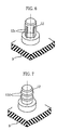
- each of the pins 12 maybe integrally formed with a plurality of axially extending ribs 12c.
- the pin 12 may be integrally formed with a plurality of annular ribs 12d, as shown in Fig. 7.
- the pin may be further provided with such slits as illustrated in Fig. 5.
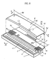
- Fig. 8 schematically shows a thermal printhead in accordance with a second embodiment of the present invention.
- the thermal printhead of the second embodiment includes a heat sink plate 1', a head substrate 2' and a circuit board 3'.
- the heat sink plate 1' is made of a metal such as aluminum.
- the heat sink plate 1' has a rectangular upper surface which is formed with a longitudinally extending groove 1a'. As shown in Fig. 9, the groove 1a' divides the upper surface of the heat sink plate 1' into a first region 1b' and a second region 1c'.
- the head substrate 2' is made of a ceramic material and bonded to the first region 1b' with an adhesive.
- the circuit board 3' is bonded to the second region 1c' with an adhesive.
- the head substrate 2' has an upper surface formed with a linear heating resistor 4' extending longitudinally of the head substrate.
- the upper surface of the head substrate 2' is further formed with a plurality of drive ICs 5' arranged in an array extending longitudinally of the upper surface for driving the heating resistor 4' (See Fig. 9).
- the drive ICs 5' are covered with a coating layer 6' formed of a synthetic resin.
- a connector 7' is mounted to the circuit board 3' for connection to external circuits.
- the upper surface of the circuit board 3' is formed with a wiring pattern (not shown) for connecting the connector 7' to the drive ICs 5'.
- a plurality of lead terminals 8' bridge between the head substrate 2' and the circuit board 3'.
- the lead terminals electrically connect the wiring pattern of the circuit board 3' to the drive ICs 5'.
- the upper surface of the circuit board 3' is covered with a protective cover 9'.
- the protective cover 9' also covers the plurality of drive ICs 5' partially.
- the protective cover 9' is formed of a heat-resistant synthetic resin.
- the protective cover 9' has an elongated main body which is warped longitudinally in a natural state. Specifically, as shown in Fig. 10, the protective cover 9' is formed so that, as viewed longitudinally of the protective cover 9', a central portion of the main body is located slightly higher than both ends.
- the protective cover 9' is provided, on the reverse surface thereof, with first engagement pieces 9a', 9b' which are integrally formed on the main body of the protective cover 9'.
- the circuit board 3' has cutouts 3a', 3b' provided correspondingly to the respective engagement pieces .
- the distance L1 between the engagement pieces 9a', 9b' is made slightly shorter than the distance L0 between the cutouts 3a', 3b'.
- the protective cover 9' is further provided, on the reverse surface thereof, with two protrusions 9c' which are integrally formed on the main body of the protective cover 9'.
- the circuit board 3' is formed with two through-holes 3c' provided correspondingly to the respective protrusions.
- the protective cover 9' is further provided, on the reverse surface thereof, with two second engagement pieces 9d' which are integrally formed on the main body of the protective cover 9'. As shown in Fig. 9, each of the second engagement pieces 9d' is L-shaped.
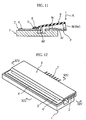
- the protective cover 9' is mounted to the circuit board 3' in the following manner. As shown in Fig. 11, the second engagement pieces 9d' are brought into engagement with the head substrate 2' . Then, the protective cover 9' is pressed in the direction of an arrow A until the first engagement pieces 9a', 9b' engage the cutouts 3a',3b', respectively. In this way, the protective cover 9' is fixed to the circuit board 3' (See Figs. 12 and 13).
- the central portion of the protective cover 9' is held higher than the both ends even when the protective cover 9' is mounted to the circuit board 3', as shown in Fig. 14. with such an arrangement, a printing paper and/or an ink ribbon comes into contact with the central portion of the protective cover 9' relatively strongly. As a result, it is possible to prevent the printing paper and/or the ink ribbon from being broken or wrinkled.
- the protective cover 9' described above is slightly warped (See Fig. 14)
- the protective cover 9' may be arranged so as to be substantially planar when mounted to the circuit board 3'. In that case, the length of protrusions 9c' are made shorter than those shown in Fig. 14.
- each of the protrusions 9c' is received in a corresponding through-hole 3c' .
- the protective cover 9' is prevented from being displaced from its position relative to the protective circuit 3'.
- the second engagement pieces 9d' are kept in engagement with the lower surface of the head substrate 2', it is possible to avoid undesirable removal of the protective cover 9' from the head substrate 2'.
Landscapes
- Electronic Switches (AREA)
Abstract
Description
Claims (18)
- A protective cover for use in a thermal printhead including a heat sink plate formed with a plurality of fixing holes, a head substrate, and a circuit board, the protective cover comprising:a main body having an obverse surface and a reverse surface; anda plurality of pins extending from the reverse surface;
wherein each of the pins is arranged for press-fitting into a respective one of the fixing holes. - The protective cover according to claim 1, wherein the pins are integrally formed on the main body.
- The protective cover according to claim 1, wherein each of the pins is formed with at least one slit.
- The protective cover according to claim 1, further comprising a plurality of engagement pawls for engaging the head substrate, each of the engagement pawls being integrally formed on the main body.
- The protective cover according to claim 4, wherein each of the engagement pawls extends in the same direction as the pins.
- The protective cover according to claim 4, further comprising a plurality of protrusions projecting from the reverse surface of the main body, each of the protrusions being provided adjacent to a respective one of the engagement pawls.
- A thermal printhead comprising:a heat sink plate formed with a plurality of fixing holes;a head substrate carried on the heat sink plate and provided with a heating resistor and a plurality of drive ICs;a circuit board carried on the heat sink plate and formed with a predetermined wiring pattern; anda protective cover for covering the circuit board, the protective cover having a main body including an obverse surface and a reverse surface;
wherein the protective cover has a plurality of pins extending from the reverse surface of the main body, each of the pins being designed for press-fitting into a respective one of the fixing holes in the heat sink plate. - A protective cover for use with a thermal printhead including a heat sink plate, a head substrate, and a circuit board, the protective cover comprising:an elongated main body including an obverse surface and a reverse surface;
wherein the main body is warped so that a longitudinally central portion of the main body is located higher than other portions of the main body - The protective cover according to claim 8, further comprising a plurality of first engagement pieces protruding from the reverse surface of the main body for engagement with the circuit board.
- The protective cover according to claim 8, further comprising a plurality of protrusions protruding from the reverse surface of the main body for engagement with the heat sink plate.
- The protective cover according to claim 9, further comprising a plurality of second engagement pieces protruding from the reverse surface of the main body for engagement with the head substrate.
- The protective cover according to claim 10, wherein the protrusions are integrally formed on the main body.
- A thermal printhead comprising:a heat sink plate;a head substrate carried on the heat sink plate and provided with a heating resistor and a plurality of drive ICs;a circuit board carried on the heat sink plate and formed with a predetermined wiring pattern; anda protective cover for covering the circuit board, the protective cover having an elongated main body including an obverse surface and a reverse surface;
wherein the main body is warped so that a longitudinally central portion of the main body is located higher than other portions of the main body. - The thermal printhead according to claim 13, wherein the main body of the protective cover is provided with a plurality of protrusions for engagement with the heat sink plate.
- The thermal printhead according to claim 14, wherein the circuit board is formed with a plurality of through-holes for allowing passage of the protrusions.
- The thermal printhead according to claim 13, wherein the protective cover is provided with a plurality of first engagement pieces protruding from the reverse surface of the main body for engagement with the circuit board.
- The thermal printhead according to claim 16, wherein the circuit board includes cutouts for engagement with the first engagement pieces.
- The thermal printhead according to claim 13, wherein the protective cover is provided with a plurality of second engagement pieces protruding from the reverse surface of the main body for engagement with the head substrate.
Applications Claiming Priority (3)
| Application Number | Priority Date | Filing Date | Title |
|---|---|---|---|
| JP01952298A JP3238893B2 (en) | 1998-01-30 | 1998-01-30 | Cover device in thermal print head |
| JP1952298 | 1998-01-30 | ||
| PCT/JP1999/000372 WO1999038696A1 (en) | 1998-01-30 | 1999-01-28 | Thermal printing head and protective cover used for the same |
Publications (3)
| Publication Number | Publication Date |
|---|---|
| EP1052102A1 true EP1052102A1 (en) | 2000-11-15 |
| EP1052102A4 EP1052102A4 (en) | 2001-05-02 |
| EP1052102B1 EP1052102B1 (en) | 2010-04-21 |
Family
ID=12001685
Family Applications (1)
| Application Number | Title | Priority Date | Filing Date |
|---|---|---|---|
| EP99901905A Expired - Lifetime EP1052102B1 (en) | 1998-01-30 | 1999-01-28 | Thermal printing head and protective cover used for the same |
Country Status (7)
| Country | Link |
|---|---|
| US (1) | US6236422B1 (en) |
| EP (1) | EP1052102B1 (en) |
| JP (1) | JP3238893B2 (en) |
| KR (1) | KR100346743B1 (en) |
| CA (1) | CA2317408C (en) |
| DE (1) | DE69942270D1 (en) |
| WO (1) | WO1999038696A1 (en) |
Cited By (1)
| Publication number | Priority date | Publication date | Assignee | Title |
|---|---|---|---|---|
| DE10018797B4 (en) * | 1999-04-13 | 2005-07-28 | Rohm Co. Ltd. | Protective cover for a thermal printhead and thermal printhead with this protective cover |
Families Citing this family (6)
| Publication number | Priority date | Publication date | Assignee | Title |
|---|---|---|---|---|
| JP4323022B2 (en) * | 1999-09-21 | 2009-09-02 | ローム株式会社 | Manufacturing method of thermal print head |
| FR2837424B1 (en) * | 2002-03-21 | 2004-09-10 | A P S Engineering | THERMAL PRINTHEAD OF WHICH THE PRINTING TAPE GUIDE BODY IS AGENCED TO ALLOW EARTHING OF THE PRINTHEAD |
| KR100601725B1 (en) | 2005-06-10 | 2006-07-18 | 삼성전자주식회사 | Thermal Image Forming Device |
| KR200447161Y1 (en) * | 2007-12-11 | 2009-12-29 | 한양특허법인 | Electronic door lock open / lock button protection cover |
| US8310511B2 (en) * | 2009-05-08 | 2012-11-13 | Rohm Co., Ltd. | Thermal printhead |
| JP6269009B2 (en) * | 2013-12-12 | 2018-01-31 | セイコーエプソン株式会社 | Recording device |
Family Cites Families (7)
| Publication number | Priority date | Publication date | Assignee | Title |
|---|---|---|---|---|
| JPH01275066A (en) * | 1988-04-26 | 1989-11-02 | Nec Corp | Thermal head |
| JP2793230B2 (en) * | 1989-03-01 | 1998-09-03 | 京セラ株式会社 | Thermal head |
| JPH05162348A (en) | 1991-12-13 | 1993-06-29 | Aoi Denshi Kk | Thermal printing head |
| JP3248828B2 (en) | 1995-03-22 | 2002-01-21 | ローム株式会社 | Thermal printhead structure |
| CN1056339C (en) | 1994-10-03 | 2000-09-13 | 罗姆股份有限公司 | thermal print head |
| JPH0994988A (en) | 1995-09-29 | 1997-04-08 | Kyocera Corp | Thermal head |
| JP3242359B2 (en) * | 1997-12-25 | 2001-12-25 | ローム株式会社 | Cover device in thermal print head |
-
1998
- 1998-01-30 JP JP01952298A patent/JP3238893B2/en not_active Expired - Fee Related
-
1999
- 1999-01-28 EP EP99901905A patent/EP1052102B1/en not_active Expired - Lifetime
- 1999-01-28 CA CA002317408A patent/CA2317408C/en not_active Expired - Fee Related
- 1999-01-28 DE DE69942270T patent/DE69942270D1/en not_active Expired - Lifetime
- 1999-01-28 KR KR1020007008008A patent/KR100346743B1/en not_active Expired - Fee Related
- 1999-01-28 US US09/600,959 patent/US6236422B1/en not_active Expired - Fee Related
- 1999-01-28 WO PCT/JP1999/000372 patent/WO1999038696A1/en not_active Ceased
Cited By (1)
| Publication number | Priority date | Publication date | Assignee | Title |
|---|---|---|---|---|
| DE10018797B4 (en) * | 1999-04-13 | 2005-07-28 | Rohm Co. Ltd. | Protective cover for a thermal printhead and thermal printhead with this protective cover |
Also Published As
| Publication number | Publication date |
|---|---|
| KR100346743B1 (en) | 2002-08-03 |
| KR20010034293A (en) | 2001-04-25 |
| EP1052102B1 (en) | 2010-04-21 |
| WO1999038696A1 (en) | 1999-08-05 |
| JPH11216893A (en) | 1999-08-10 |
| CA2317408A1 (en) | 1999-08-05 |
| EP1052102A4 (en) | 2001-05-02 |
| JP3238893B2 (en) | 2001-12-17 |
| US6236422B1 (en) | 2001-05-22 |
| DE69942270D1 (en) | 2010-06-02 |
| CA2317408C (en) | 2004-04-27 |
Similar Documents
| Publication | Publication Date | Title |
|---|---|---|
| JP3228974B2 (en) | Line type thermal print head | |
| EP1052102B1 (en) | Thermal printing head and protective cover used for the same | |
| EP1557275A2 (en) | Thermal head | |
| JP7309040B2 (en) | Thermal head and thermal printer | |
| CA2431536C (en) | Thermal printhead and protective cover used for the same | |
| CN115315356A (en) | Thermal head and thermal printer | |
| US20070040868A1 (en) | Thermal printhead | |
| CN115362066B (en) | Thermal head and thermal printer | |
| EP0729840B1 (en) | Ic for driving printer and print head | |
| JP2562880B2 (en) | Thermal head | |
| JPS63111064A (en) | Thermal head | |
| JPH11129513A (en) | Thermal head | |
| JP3242359B2 (en) | Cover device in thermal print head | |
| JPH08258309A (en) | Structure of thermal print head | |
| US11945233B2 (en) | Thermal head and thermal printer | |
| JPH11157110A (en) | Thermal head | |
| JPS60232975A (en) | Thick film type thermal recording head | |
| JPH09150540A (en) | Thermal head | |
| JP2025166287A (en) | Thermal head, printer | |
| KR0151095B1 (en) | Thermal recording element | |
| JP2568086Y2 (en) | Thermal head | |
| JP3017157B2 (en) | Thermal printhead structure | |
| JP2005186345A (en) | Thermal head and thermal printer using the same | |
| JPH05177854A (en) | Thermal head | |
| JPH05147249A (en) | Thermal head |
Legal Events
| Date | Code | Title | Description |
|---|---|---|---|
| PUAI | Public reference made under article 153(3) epc to a published international application that has entered the european phase |
Free format text: ORIGINAL CODE: 0009012 |
|
| 17P | Request for examination filed |
Effective date: 20000727 |
|
| AK | Designated contracting states |
Kind code of ref document: A1 Designated state(s): DE FR GB IT |
|
| A4 | Supplementary search report drawn up and despatched |
Effective date: 20010320 |
|
| AK | Designated contracting states |
Kind code of ref document: A4 Designated state(s): DE FR GB IT |
|
| 17Q | First examination report despatched |
Effective date: 20061206 |
|
| GRAP | Despatch of communication of intention to grant a patent |
Free format text: ORIGINAL CODE: EPIDOSNIGR1 |
|
| GRAS | Grant fee paid |
Free format text: ORIGINAL CODE: EPIDOSNIGR3 |
|
| GRAA | (expected) grant |
Free format text: ORIGINAL CODE: 0009210 |
|
| AK | Designated contracting states |
Kind code of ref document: B1 Designated state(s): DE FR GB IT |
|
| REG | Reference to a national code |
Ref country code: GB Ref legal event code: FG4D |
|
| REF | Corresponds to: |
Ref document number: 69942270 Country of ref document: DE Date of ref document: 20100602 Kind code of ref document: P |
|
| PLBE | No opposition filed within time limit |
Free format text: ORIGINAL CODE: 0009261 |
|
| STAA | Information on the status of an ep patent application or granted ep patent |
Free format text: STATUS: NO OPPOSITION FILED WITHIN TIME LIMIT |
|
| 26N | No opposition filed |
Effective date: 20110124 |
|
| PG25 | Lapsed in a contracting state [announced via postgrant information from national office to epo] |
Ref country code: IT Free format text: LAPSE BECAUSE OF FAILURE TO SUBMIT A TRANSLATION OF THE DESCRIPTION OR TO PAY THE FEE WITHIN THE PRESCRIBED TIME-LIMIT Effective date: 20100421 |
|
| GBPC | Gb: european patent ceased through non-payment of renewal fee |
Effective date: 20110128 |
|
| REG | Reference to a national code |
Ref country code: FR Ref legal event code: ST Effective date: 20110930 |
|
| PG25 | Lapsed in a contracting state [announced via postgrant information from national office to epo] |
Ref country code: FR Free format text: LAPSE BECAUSE OF NON-PAYMENT OF DUE FEES Effective date: 20110131 |
|
| PG25 | Lapsed in a contracting state [announced via postgrant information from national office to epo] |
Ref country code: GB Free format text: LAPSE BECAUSE OF NON-PAYMENT OF DUE FEES Effective date: 20110128 |
|
| PGFP | Annual fee paid to national office [announced via postgrant information from national office to epo] |
Ref country code: DE Payment date: 20120125 Year of fee payment: 14 |
|
| PG25 | Lapsed in a contracting state [announced via postgrant information from national office to epo] |
Ref country code: DE Free format text: LAPSE BECAUSE OF NON-PAYMENT OF DUE FEES Effective date: 20130801 |
|
| REG | Reference to a national code |
Ref country code: DE Ref legal event code: R119 Ref document number: 69942270 Country of ref document: DE Effective date: 20130801 |