EP1049172A2 - A SOI structure semiconductor device and a fabrication method thereof - Google Patents
A SOI structure semiconductor device and a fabrication method thereof Download PDFInfo
- Publication number
- EP1049172A2 EP1049172A2 EP00104155A EP00104155A EP1049172A2 EP 1049172 A2 EP1049172 A2 EP 1049172A2 EP 00104155 A EP00104155 A EP 00104155A EP 00104155 A EP00104155 A EP 00104155A EP 1049172 A2 EP1049172 A2 EP 1049172A2
- Authority
- EP
- European Patent Office
- Prior art keywords
- layer
- soi
- silicon substrate
- oxide layer
- silicon
- Prior art date
- Legal status (The legal status is an assumption and is not a legal conclusion. Google has not performed a legal analysis and makes no representation as to the accuracy of the status listed.)
- Granted
Links
Images





Classifications
-
- H—ELECTRICITY
- H10—SEMICONDUCTOR DEVICES; ELECTRIC SOLID-STATE DEVICES NOT OTHERWISE PROVIDED FOR
- H10P—GENERIC PROCESSES OR APPARATUS FOR THE MANUFACTURE OR TREATMENT OF DEVICES COVERED BY CLASS H10
- H10P90/00—Preparation of wafers not covered by a single main group of this subclass, e.g. wafer reinforcement
- H10P90/19—Preparing inhomogeneous wafers
- H10P90/1904—Preparing vertically inhomogeneous wafers
- H10P90/1906—Preparing SOI wafers
-
- H—ELECTRICITY
- H10—SEMICONDUCTOR DEVICES; ELECTRIC SOLID-STATE DEVICES NOT OTHERWISE PROVIDED FOR
- H10W—GENERIC PACKAGES, INTERCONNECTIONS, CONNECTORS OR OTHER CONSTRUCTIONAL DETAILS OF DEVICES COVERED BY CLASS H10
- H10W10/00—Isolation regions in semiconductor bodies between components of integrated devices
- H10W10/01—Manufacture or treatment
- H10W10/061—Manufacture or treatment using SOI processes together with lateral isolation, e.g. combinations of SOI and shallow trench isolations
-
- H—ELECTRICITY
- H10—SEMICONDUCTOR DEVICES; ELECTRIC SOLID-STATE DEVICES NOT OTHERWISE PROVIDED FOR
- H10W—GENERIC PACKAGES, INTERCONNECTIONS, CONNECTORS OR OTHER CONSTRUCTIONAL DETAILS OF DEVICES COVERED BY CLASS H10
- H10W10/00—Isolation regions in semiconductor bodies between components of integrated devices
- H10W10/10—Isolation regions comprising dielectric materials
- H10W10/181—Semiconductor-on-insulator [SOI] isolation regions, e.g. buried oxide regions of SOI wafers
-
- H—ELECTRICITY
- H10—SEMICONDUCTOR DEVICES; ELECTRIC SOLID-STATE DEVICES NOT OTHERWISE PROVIDED FOR
- H10P—GENERIC PROCESSES OR APPARATUS FOR THE MANUFACTURE OR TREATMENT OF DEVICES COVERED BY CLASS H10
- H10P14/00—Formation of materials, e.g. in the shape of layers or pillars
- H10P14/60—Formation of materials, e.g. in the shape of layers or pillars of insulating materials
- H10P14/61—Formation of materials, e.g. in the shape of layers or pillars of insulating materials using masks
-
- H—ELECTRICITY
- H10—SEMICONDUCTOR DEVICES; ELECTRIC SOLID-STATE DEVICES NOT OTHERWISE PROVIDED FOR
- H10P—GENERIC PROCESSES OR APPARATUS FOR THE MANUFACTURE OR TREATMENT OF DEVICES COVERED BY CLASS H10
- H10P90/00—Preparation of wafers not covered by a single main group of this subclass, e.g. wafer reinforcement
- H10P90/19—Preparing inhomogeneous wafers
- H10P90/1904—Preparing vertically inhomogeneous wafers
- H10P90/1906—Preparing SOI wafers
- H10P90/1908—Preparing SOI wafers using silicon implanted buried insulating layers, e.g. oxide layers [SIMOX]
-
- H—ELECTRICITY
- H10—SEMICONDUCTOR DEVICES; ELECTRIC SOLID-STATE DEVICES NOT OTHERWISE PROVIDED FOR
- H10W—GENERIC PACKAGES, INTERCONNECTIONS, CONNECTORS OR OTHER CONSTRUCTIONAL DETAILS OF DEVICES COVERED BY CLASS H10
- H10W10/00—Isolation regions in semiconductor bodies between components of integrated devices
- H10W10/01—Manufacture or treatment
- H10W10/011—Manufacture or treatment of isolation regions comprising dielectric materials
- H10W10/012—Manufacture or treatment of isolation regions comprising dielectric materials using local oxidation of silicon [LOCOS]
-
- H—ELECTRICITY
- H10—SEMICONDUCTOR DEVICES; ELECTRIC SOLID-STATE DEVICES NOT OTHERWISE PROVIDED FOR
- H10W—GENERIC PACKAGES, INTERCONNECTIONS, CONNECTORS OR OTHER CONSTRUCTIONAL DETAILS OF DEVICES COVERED BY CLASS H10
- H10W10/00—Isolation regions in semiconductor bodies between components of integrated devices
- H10W10/10—Isolation regions comprising dielectric materials
- H10W10/13—Isolation regions comprising dielectric materials formed using local oxidation of silicon [LOCOS], e.g. sealed interface localised oxidation [SILO] or side-wall mask isolation [SWAMI]
Definitions
- This invention relates to a semiconductor device using a SOI (Silicon On Insulator) substrate and a fabrication method thereof, and more particularly to a device structure in which this feature is employed in the silicon layer portion of the semiconductor device.
- SOI Silicon On Insulator
- a silicon layer is formed on a layer with insulation properties, a so-called BOX oxide layer.
- This silicon layer is isolated by a trench structure or a LOCOS (Local Oxidation Of Silicon) method in order to isolate the device.
- LOCOS Local Oxidation Of Silicon
- the trench method in which a groove is formed by the silicon layer being etched and an oxide layer being deposited in the groove is disclosed in "IEEE ELECTRON DEVICE LETTERS; VOL. 6, JUNE, 1995,” and others.
- the cost of isolation using the trench structure is high because the number of processes required for trench structure formation is greater than the LOCOS method.
- the device isolation for SOI by the LOCOS method is disclosed in "Proceedings IEEE Intr. SOI conf., 116 (1995).”
- a thin silicon layer the sectional shape of which is a triangle is formed between a LOCOS oxide layer and a BOX oxide layer and this layer forms the parasite MOSFET.
- This parasite MOSFET influences significantly the current property of the original (on the assumption that there is no MOSFET) MOSFET. This influence is called a bump property because it looks like a bump is made on the current properties.
- the threshold voltage for which the parasite MOSFET exists is lower than the original MOSFET.
- the object of the present invention is to provide a semiconductor device of SOI structure and a fabrication method thereof avoiding formation of a parasite MOSFET.
- a SOI structure semiconductor device is characterized as claimed in claim 1, the subclaims defining preferred embodiments of this SOI structure semiconductor device.
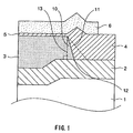
- FIG. 1 is a part of a sectional view of a SOI device structure of the first preferred embodiment of the present invention.
- a SOI layer 3 is a silicon layer, the thickness of which is 400 to 500 angstroms is formed on a BOX oxide layer 2, the thickness of which is approximately 400 to 500 angstroms, which is formed on a silicon substrate 1.
- a part of the SOI layer 3 is oxidized by a LOCOS method and becomes a LOCOS oxide layer 4, the layer thickness of which is approximately 400 angstroms.
- a gate oxide layer 5 the layer thickness of which is relatively thin (in the vicinity of approximately 70 angstroms) is formed on the SOI layer 3.
- the boundary 10 between the SOI layer 3 and the LOCOS oxide layer 4 has a shape more likely to be perpendicular than the conventional boundary line 11.
- the ratio of the base (the boundary 12) to the height (the perpendicular line 13) of the triangle portion formed by the boundary 12 between the BOX oxide layer 2 and the SOI layer 3, a perpendicular line 13 of the SOI layer 3 in the thickness direction, and the distance from a cross point of the perpendicular line and the bottom of the SOI layer 3 to the boundary 10 between the SOI layer 3 and the LOCOS oxide layer 4 is determined as 1 : 4 or the ratio of the base itself is less than this.
- Figure 2 is a view showing simulation results of a current voltage characteristic of a SOI device structure of the first preferred embodiment. Drain current Id is plotted on the vertical axis and gate bias current Vg is plotted on the horizontal axis.
- 1e-05 means 1 ⁇ 10 -5 .
- the off-leak current of the current property "B" of the first embodiment is restrained within one digit.
- the current properties "C" where the ratio of the base to the height of the triangle portion of SOI structure is 1 : 1 1, a remarkable improvement is apparent and it is possible to verify according to FIG. 2 that this is the same as the ideal current property "A".
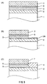
- Figures 3(A) to 3(C) are sectional views showing a fabrication method of a SOI device structure of the first preferred embodiment. Referring to these Figures, a fabrication method of a SOI device structure of the first preferred embodiment is explained hereinafter.
- a SIMOX (Separation by Implementation of Oxygen) substrate is prepared in which the BOX oxide layer 2 the layer thickness of which is approximately 1000 to 1500 angstroms and the SOI layer 3 the layer thickness of which is approximately 500 angstroms are layered and formed.
- the gate oxide layer 5 the layer thickness of which is 70 angstroms and a nitride layer 7 the layer thickness of which is 500 angstroms are successively formed on the SOI layer 3 of the SIMOX substrate (Fig. 3(A)).
- the layer thickness of the SOI layer 3 decreases to approximately 400 angstroms due to the gate oxide layer 5 being formed, successive processing, and so forth.
- a part of the SOI layer 3, the gate oxide layer 5, and the nitride layer 7 of the portion composing the LOCOS oxide layer is eliminated (Fig. 3(B)).
- the volume of the BOX oxide layer 2 eliminated is approximately 300 angstroms which is 3/4 of the original layer thickness of approximately 400 angstroms.
- the layer thickness of a SOI layer 3A after elimination becomes 100 angstroms which is 1/4 of the layer thickness of the original SOI layer 3.
- the SOI layer 3A is transformed to the LOCOS oxide layer 4 by implementation of the LOCOS oxide process (Fig. 3(C)).
- the triangle portion of the SOI layer 2 formed in the boundary portion between the BOX oxide layer 2 and the transformed SOI layer 3 decreases and the ratio of the base to the height becomes 1 : 4 or the ratio of the base becomes smaller.
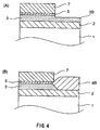
- Figures 4(A) and 4(B) are sectional views showing fabrication processes contrasting with the first preferred embodiment.
- the process of Fig. 4(A) corresponds to Fig. 3(B) and the volume of the SOI layer 3 eliminated is defined as approximately 80 angstroms which is 1/5 of the original layer thickness of approximately 400 angstroms.
- the layer thickness of a SOI layer 3B after elimination becomes approximately 320 angstroms which is 4/5 of the layer thickness of the original SOI layer 3.
- the SOI layer 3B is transformed to a LOCOS oxide layer 4B by implementation of the LOCOS oxide process (Fig.4(B)).
- the triangle portion of the SOI layer 3 formed in the boundary portion between the SOI layer 3 and the transformed LOCOS oxide layer 4 B grows far into the LOCOS oxide layer 4 B, thus the ratio of the base to the height becomes approximately 1 : 1.
- the volume ratio of silicon eroded into the oxide layer and extending upward is 0.44 : 0.56. Because of this, when the layer thickness of the SOI layer 3A transformed into the LOCOS oxide layer 4 is thin, the length (the volume of the portion extending into the LOCOS oxide layer 4) of the base of the triangle portion of the boundary portion can be kept short.
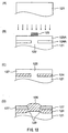
- Figures 5(A) to 5(C) are sectional views showing another fabrication method of a SOI device structure of the first preferred embodiment. Referring to these figures, another fabrication method of a SOI device structure of the first preferred embodiment is explained.
- the SIMOX substrate is prepared, in which the SOI layer 3 the layer thickness of which is approximately 500 angstroms and the BOX oxide layer 2 the layer thickness of which is approximately 1000 to 1500 angstroms are layered and formed on the silicon substrate.
- the gate oxide layer 5 the layer thickness of which is approximately 70 angstroms and the nitride layer 7 the layer thickness of which is approximately 500 angstroms are formed successively on the SOI layer 3 of the SIMOX substrate (Fig. 5(A)).
- the layer thickness of the SOI layer 3 decreases to approximately 400 angstroms because of the formation of the gate oxide layer 5 and the subsequent processing implemented.
- the part of the nitride layer 7 forming the LOCOS oxide layer, the gate oxide layer 5, and the SOI layer 3 is removed.
- the nitride layer 7, the gate oxide layer 5, and the SOI layer 3 are eliminated by oblique etching (Fig. 5(B)).
- the oblique etching may be implemented by a reactive ion etching method, etc.
- etching is implemented as far as approximately 3/4 of the original layer thickness as already explained in the fabrication method shown in Fig. 3.
- the volume of the SOI layer 3 being eliminated depends on the etching condition, it is appropriate that layer, the thickness of which is approximately 200 angstroms which is approximately 1/2 of the original layer thickness is eliminated.
- a part of the SOI layer 3C is transformed to the LOCOS oxide layer 4C by implementation of the LOCOS oxide process. Since the triangle portion of the SOI layer 3 formed in the boundary portion between the SOI layer 3 and the LOCOS oxide layer 4C is over-etched by oblique etching, it decreases and the ratio of the base to the height becomes 1 : 4 or the ratio of the base becomes smaller than this ratio.
- Figures 6(A) and 6(B) are partial sectional views showing a SOI device structure of the second preferred embodiment.
- a nitride layer 63 the layer thickness of which is approximately 1150 angstroms is formed on a BOX oxide layer 62 the layer thickness of which is approximately 1000 to 1500 angstroms which is formed on a silicon substrate 61.
- a SOI layer 64 the layer thickness of which is approximately 500 angstroms is formed on the nitride layer 63.
- a part of the SOI substrate 60 is oxidized by the LOCOS method and then a part of the SOI layer 64 becomes a LOCOS oxide layer 65 the layer thickness of which is approximately 400 angstroms.
- a gate oxide layer 66 the layer thickness of which is comparatively thin is formed on the SOI layer 64, and polysilicon 67 functioning as a gate is formed on a gate oxide layer 66 (Fig. 6(B)).
- the SOI layer 3 When the SOI layer 3 is oxidized and transformed to the LOCOS oxide layer 4, according to the conventional method, the LOCOS oxide layer forms and is connected to the BOX oxide layer 2.
- the SOI layer 3 as the device portion (channel portion) is then oxidized in the upward direction from the BOX oxide layer 2.
- the SOI layer 3 becomes a so-called floating state, as the simulation results indicate.
- Fig. 7(A) and Fig. 7(B) which is a sectional view of the main parts of Fig. 7(A)
- a thin SOI layer is formed in the boundary portion between the SOI layer 3 and the LOCOS oxide layer 4.
- the nitride layer 63 is formed on the BOX oxide layer 62. Since the nitride layer does not accelerate oxidization of the silicon layer to the oxide layer, it cannot be verified that the phenomenon in which the SOI layer 64 of the device portion (channel portion) is oxidized in the upward direction from the nitride layer 63 does not occur. Thus, as the simulation results indicate as shown in Fig. 7(C) and Fig. 7(D) which is a sectional view of main parts of FIG. 7(C), since oxidization from the lower portion is not implemented even in the boundary portion between the SOI layer 65 and the SOI layer 64, the SOI layer 64 is formed comparatively thick.
- the nitride layer 63 is formed between the BOX oxide layer 62 and the SOI layer 64, oxidation the direction of which is from the lower portion of the SOI layer 64 is capable of being restrained.
- the layer thickness of the SOI layer 64 of the boundary portion between the SOI layer 64 and the LOCOS oxide layer 65 is therefore capable of being maintained.
- the BOX oxide layer 62 is under the nitride layer 63, it is expected that leakage problems based on the rigid properties of the nitride layer can be decreased by stress relaxation due to the oxide layer.
- Figures 8(A) to 8(D) are sectional views showing a fabrication method of a SOI device structure of the second embodiment. Referring to these figures, a fabrication method of a SOI device structure of the second preferred embodiment is explained.
- an oxygen ion is injected into the silicon substrate 61 (Fig. 8 (A)) which has already been prepared.
- An oxygen containing layer 62A is formed in a predetermined deep portion of the silicon substrate 61 by this ion injection, and a silicon layer 64A remains on the surface (Fig. 8 (B)).
- the oxygen ion injection is controlled in order for the oxygen containing layer 62A to be formed in a portion the depth of which is approximately 1650 to 3150 angstroms.
- a nitride ion is injected into the silicon substrate 61 in which the oxygen containing layer 62A has been formed.
- a nitride containing layer 63A is formed on the oxygen containing layer 62A by this ion injection (Fig.
- the nitride ion injection is controlled to control the layer thickness of the nitride containing layer 63A at approximately 1150 angstroms, which is 500 to 1650 angstroms from the surface.
- the oxygen containing layer 62A is transformed into the BOX oxide layer 62
- the nitride containing layer 63A is transformed into the nitride layer 63
- the SOI substrate that is a prerequisite to Fig. 6 (A) is formed by the application of heat treatment (Fig. 8 (D)).
- Figures 9(A) and 9(B) are partial sectional views of a SOI device structure of the third preferred embodiment.
- a nitride layer 93 the thickness of which is approximately 1150 angstroms is formed as a SOI substrate 90 employed in the preferred embodiment.
- a SOI layer 94 the layer thickness of which is approximately 500 angstroms is formed on the nitride layer 93.
- a part of the SOI substrate 90 employed in the third preferred embodiment is oxidized by the LOCOS method, and a part of the SOI layer 94 becomes a LOCOS oxide layer 95 the layer thickness of which is 400 angstroms.
- a comparatively thin gate oxide layer 96 the layer thickness of which is approximately 70 angstroms is formed on the SOI layer 94.
- the thin SOI layer 3 is formed in the boundary portion between the SOI layer 3 and the LOCOS oxide layer 4.
- the nitride layer 93 is formed on the SOI substrate employed in the third embodiment instead of the BOX oxide layer 2. Since the nitride layer does not accelerate oxidization of the silicon layer to the oxide layer, a phenomenon in which the SOI layer 94 as the device portion (channel portion) is oxidized in the upward direction from the nitride layer 93 does not occur. Thus, as indicated in the simulation results shown in Fig. 10 (A) and Fig. 10(B) which is the enlarged portion of Fig. 10(A), since the boundary portion between the SOI layer 94 and the LOCOS oxide layer 95 is not oxidized in the direction from the lower portion, the SOI layer 94 is formed comparatively thick.
- the nitride layer 93 is formed in the third preferred embodiment instead of the BOX oxide layer, oxidation in the direction from the lower portion of the SOI layer 94 may be restrained. The result of this is the layer thickness of the SOI layer 94 in the boundary portion between the SOI layer 94 and the LOCOS oxide layer 95 may be maintained. Further, since the conventional BOX oxide layer is simply converted to the nitride layer, the fabricating processes do not increase and implementation may be easily done.
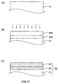
- FIGS 11(A) to 11(C) are sectional views showing a fabrication method of a SOI substrate of the third preferred embodiment. Referring to these Figures, the fabrication method of the SOI substrate employed in the third embodiment is explained.
- the nitride ion is injected into a prepared silicon substrate 9 (Fig. 11(A)). Due to this ion injection, a nitride containing layer 93A is formed in a predetermined deep portion of the silicon substrate 61, and a silicon layer 94A remains on the surface (Fig. 11(B)). The nitride ion injection is controlled so that the nitride containing layer 93A is formed in a portion the depth of which is approximately 500 angstroms to 1650 angstroms from the surface.
- the nitride injection is controlled so that the layer thickness of the nitride containing layer 93A is approximately 1150 angstroms.
- the nitride containing layer 93A is transformed to the nitride layer 93 by heat treatment, and the SOI substrate 90 that is a prerequisite to Fig. 9(A) is formed (Fig. 11(C)).
- the fabrication method of the SOI substrate employed in the third embodiment has an advantage where unexpected chemical reactions of oxygen, nitrogen and others can be avoided, compared with the fabrication method of the SOI substrate employed in the second preferred embodiment. Further, since the ion injection is applied only once, advantages exist as the processes are simplified and the processing cost is therefore reduced.
- Figures 12(A) to 12(D) are sectional views showing a fabrication method of a SOI device of the fourth preferred embodiment. Referring to these figures, the fabrication method of the SOI device of the fourth preferred embodiment is explained.
- a mask layer 123 is formed on a marginally larger area than a field oxide layer forming plan area 122 of the prepared silicon substrate 121 (Fig. 12(A)).
- the mask layer 123 is not limited provided it does not allow passage of oxygen ions.
- the oxygen ion is injected into the silicon substrate 121 in which this mask layer 123 is formed. Due to this ion injection, the oxygen containing layer 124A is formed in a predetermined deep portion of the silicon substrate 121 except the portion in which the mask layer 123 is formed, and a silicon layer 125A remains on the surface (Fig. 12(B)).
- the oxygen ion injection is controlled so that the oxygen containing layer 124A is formed in a portion the depth of which is approximately 1650 to 3150 angstroms from the surface of the silicon substrate 121.
- the oxygen containing layer 124A is then transformed to a BOX oxide layer 124 (Fig. 12(C)) by application of heat treatment. Due to this heat treatment, when the oxygen containing layer 124A is transformed to the BOX oxide layer 124, the BOX oxide layer 124 grows in a lateral direction. Thus, the BOX oxide layer 124 is not formed in the lower portion of the field oxide layer forming plan area 122. Following this, by implementing the LOCOS oxide process, a field oxide layer 126 grows in the downward direction of the silicon substrate 121. The field oxide layer 126 will have a structure in which the BOX oxide layers 124 provided in the silicon substrate are connected (Fig. 12(D)).
- the final shape of the SOI device of the fourth embodiment will have almost the same shape as the case in which the SOI device is formed with the SIMOX substrate having the conventional BOX oxide layer.
- the end portions of the field oxide layer 126 namely, the boundary portions of the BOX oxide layer 124 formed in the silicon substrate 121 form a slit-like portion 129.
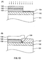
- Figures 13(A) and 13(B) are sectional views showing a fabrication method of a SOI device of the fifth preferred embodiment. Referring to these figures, the fabrication method of the SOI device of the fifth preferred embodiment is explained.
- a SIMOX substrate is prepared in which a SOI layer 133 the layer thickness of which is approximately 500 angstroms and a BOX oxide layer 132 the layer thickness of which is approximately 1000 to 1500 angstroms are layered and formed on a silicon substrate 131.
- a gate oxide layer 135 the layer thickness of which is approximately 70 angstroms and a nitride layer 136 the layer thickness of which is approximately 500 angstroms are successively formed on the SOI layer 133 of this SIMOX substrate.
- the layer thickness of the SOI layer 133 decreases to approximately 400 angstroms because of the gate oxide layer 135 forming and subsequent processing, etc.
- the volume of the SOI layer 133 eliminated is approximately 300 angstroms which is 3/4 of the original layer thickness of approximately 400 angstroms, in the same way as the fabrication method of the first preferred embodiment.
- the layer thickness of the SOI layer after elimination becomes approximately 100 angstroms which is 1/4 of the layer thickness of the original SOI layer 133.
- impurities are implanted into the whole substrate using the nitride layer 136 as the mask (Fig. 13(A)). Due to this implant, impurities are introduced into the SOI layer 134 as the field oxide layer forming plan area which then becomes a high density region.
- the SOI layer 134 is transformed to the LOCOS oxide layer 137 by implementation of the LOCOS oxide process.
- a gate polysilicon 138 is formed after the nitride layer 136 is eliminated, and the final SOI device structure is obtained (Fig. 13(B)).
- a high density region 139 is formed in the lower portion of the triangle portion of the SOI layer 133 formed in the boundary portion between the SOI layer 133 and the transformed LOCOS oxide layer 137. This is a portion of the high density region of the SOI layer 134 remaining.
- a part of the high density region does not work as a MOS because a channel portion becomes a high density region even if the parasite MOS structure is formed.
- this elimination volume is capable of being less than 3/4 because the high density region is formed.
- Figures 14(A) and 14(B) are sectional views showing a modified example of a fabrication method of a SOI device of the fifth preferred embodiment. Referring to these figures, the modified example of the fabrication method of the SOI device of the fifth preferred embodiment is explained.
- a gate oxide layer 145 and a nitride layer 147 are successively formed on the SIMOX substrate, elimination of a part of the nitride layer 147 as a LOCOS oxide layer forming plan area, a gate oxide layer 145, and a SOI layer 143 is processed in the same way as in Fig. 13(A).
- Impurities are obliquely implanted into the whole substrate using the nitride layer 147 as the mask (Fig. 14(A)). By this oblique implantation, impurities are introduced in the end portions of the SOI layer 134 as the field oxide layer forming plan area and the SOI layer 133 as the channel portion, in order to form a high density region 146.
- the high density region 146 is transformed to a LOCOS oxide layer 144 by implementation of the LOCOS oxide process. Further, a gate polysilicon 148 is formed and a final SOI device structure is attained after the nitride layer 147 is eliminated (Fig. 14(B)).
- a high density region 149 larger than the high density region 139 shown in Fig. 13(B) is formed in the lower portion of the triangle portion of the SOI layer 143 formed in the boundary portion between the SOI layer 143 and the transformed LOCOS oxide layer 144. This is because the high density region is formed in the end portion of the SOI layer 143 of the channel portion by the oblique implantation.
- the high density region does not function as MOS in the same way as shown in Fig. 13(B) because the channel portion becomes the high density region even if the parasite MOS structure is formed.
- FIG. 15 is a sectional view showing a fabrication method of a SOI device of the sixth preferred embodiment. Referring to this Figure, the fabrication method of the SOI device of the sixth preferred embodiment is explained. A SOI device is formed on the SOI substrate employed in the second preferred embodiment in the same way as the second preferred embodiment. Thus, the SOI device structure of FIG.
- FIG. 15 is the same as FIG. 6(B) except for forming the polysilicon 67.
- the fabrication method of the sixth preferred embodiment applies a threshold value control implant to the SOI device, the structure of which is shown in Fig. 6(B). Energy of this threshold value control implant is controlled so that the peak value of impurities is lower than the SOI layer 64 as shown in the graph on the right hand side of Fig. 15.
- a predetermined threshold voltage is capable of being obtained in the portion used as the channel of the SOI layer 64.
- Further implantation is possible using a combination of implantation energy and the dosing volume of impurities in order for impurity density to become higher in the SOI layer 64 and especially in the lower portion of the boundary portion of a field oxide layer.
- the SOI substrate of the sixth embodiment is the same as the SOI substrate of the second preferred embodiment, it is possible that the SOI substrate used in the third embodiment or a conventional SIMOX substrate can be used.
- Figure 16 is a sectional view showing a modified example of a fabrication method of a SOI device of the sixth preferred embodiment. Referring to the Fig. 16, the modified example of the fabrication method of the SOI device of the sixth preferred embodiment is explained.
- the SOI device is formed in the same way as the sixth preferred embodiment in which the threshold value control implant is used.
- the threshold value control implant is implemented as indicated by the reference number 160 of the graph of Fig. 16.
- a so-called counter dope in which ions the polarity of which are opposite electrically to ions used in the threshold control implant are doped, is applied with an impurity density profile as shown in the reference number 161 of the graph of Fig. 16.
- the SOI layer 64 finally displays the impurity density profile as shown by the reference number 162 of the graph of Fig. 16.
Landscapes
- Element Separation (AREA)
- Thin Film Transistor (AREA)
- Local Oxidation Of Silicon (AREA)
Abstract
Description
oxide layer and this layer forms the parasite MOSFET. This parasite MOSFET influences significantly the current property of the original (on the assumption that there is no MOSFET) MOSFET. This influence is called a bump property because it looks like a bump is made on the current properties. The threshold voltage for which the parasite MOSFET exists is lower than the original MOSFET.
As a result of this phenomenon, the
The fabrication method of the SOI substrate employed in the third embodiment has an advantage where unexpected chemical reactions of oxygen, nitrogen and others can be avoided, compared with the fabrication method of the SOI substrate employed in the second preferred embodiment. Further, since the ion injection is applied only once, advantages exist as the processes are simplified and the processing cost is therefore reduced.
FIG. 15 is a sectional view showing a fabrication method of a SOI device of the sixth preferred embodiment. Referring to this Figure, the fabrication method of the SOI device of the sixth preferred embodiment is explained.
A SOI device is formed on the SOI substrate employed in the second preferred embodiment in the same way as the second preferred embodiment. Thus, the SOI device structure of FIG. 15 is the same as FIG. 6(B) except for forming the
Claims (24)
- A SOI structure semiconductor device comprising:a silicon substrate;an insulating layer formed on said silicon substrate;a SOI layer formed on said insulating oxide layer;a LOCOS oxide layer formed on said insulating oxide layer and contacting with said SOI layer in order to insulate said SOI layer;a gate insulation layer formed on said SOI layer; anda gate electrode formed on said gate insulation layer.
- The SOI structure semiconductor device according to claim 1, wherein said SOI layer has a sectional triangle portion contacting with said LOCOS oxide layer, the sectional triangle has an oblique side as a boundary between said SOI layer and said LOCOS oxide layer , a height side equal to the thickness of said SOI layer and a base on the lower boundary of said SOI layer, in which the ratio of the height side to the base is 4:1 or less.
- The SOI structure semiconductor device according to claim 1, wherein the insulating layer formed on that silicon layer is an insulating oxide layer.
- The SOI structure semiconductor device according to claim 1, wherein the thickness of said insulating oxide layer is about 1000 to 1500 angstroms.
- The SOI structure semiconductor device of any of the claims 1 to 4 comprising:an insulating oxide layer formed on said silicon substrate;an insulating nitride layer formed on said insulating oxide layer; anda SOI layer formed on said insulating nitride layer.
- The SOI structure semiconductor device according to claim 1 or 2, wherein the insulating layer formed on said silicon layer is an insulating nitride layer.
- The SOI structure semiconductor device according to claim 4 or 5, wherein the thickness of said insulating nitride layer is about 1150 angstroms.
- A method of manufacturing a SOI structure semiconductor device comprising the steps of:providing a SOI substrate including an insulating oxide layer and a silicon layer formed on the insulating layer;forming a gate oxide layer on the silicon layer of the SOI substrate;forming a nitride layer on the gate oxide layer;selectively removing the nitride layer, gate oxide layer and a part of the silicon layer, removed thickness of which is more than ¾ of the silicon layer within a LOCOS oxide forming area;oxidizing the partly removed silicon layer within the LOCOS oxide forming area so that a LOCOS oxide layer is formed; andforming a gate electrode on the gate oxide layer.
- The method of manufacturing the SOI structure semiconductor device according to claim 8, wherein the thickness of the partly removed portion of the silicon layer is about 100 angstroms.
- The method of manufacturing the SOI structure semiconductor device according to claim 8, further comprising a step of introducing an impurity into the partly removed silicon layer within the LOCOS oxide forming area.
- The method of manufacturing the SOI structure semiconductor device according to claim 8, further comprising a step of obliquely introducing an impurity into the partly removed silicon layer within the LOCOS oxide forming area and the silicon layer adjacent to the LOCOS oxide forming area.
- A method of manufacturing a SOI structure semiconductor device comprising the steps of:providing a SOI substrate including an insulating oxide layer and a silicon layer formed on the insulating layer;forming a gate oxide layer on the silicon layer of the SOI substrate;forming a nitride layer on the gate oxide layer;obliquely removing the nitride layer, the gate oxide layer and a part of the silicon layer within a LOCOS oxide forming area so that the part of the silicon layer is removed widely than the nitride layer;oxidizing the partly removed silicon layer within the LOCOS oxide forming area so that a LOCOS oxide layer is formed; andforming a gate electrode on the gate oxide layer
- The method of manufacturing the SOI structure semiconductor device according to claim 12, wherein removed thickness of the partly removed portion of the silicon layer is about ½ of the thickness of the unremoved silicon layer;
- The method of manufacturing the SOI structure semiconductor device according to claim 8 or 12, wherein the thickness of the silicon layer of the SOI substrate is about 400 to 500 angstroms.
- The method of manufacturing the SOI structure semiconductor device according to claim 8 or 12, wherein the thickness of said insulating oxide layer of the SOI substrate is about 1000 to 1500 angstroms.
- A method of manufacturing a SOI substrate comprising steps of:providing a silicon substrate having a surface thereof;introducing oxygen ions into the silicon substrate from the surface of the silicon substrate so that an oxygen containing layer is formed in the silicon substrate positioned at a first depth from the surface of the silicon substrate,introducing nitrogen ions into the silicon substrate from the surface of the silicon substrate so that a nitrogen containing layer is formed in the silicon substrate positioned at a second depth from the surface of the silicon substrate which is closer to the surface of the silicon substrate than the first depth; andsubjecting the silicon substrate including the oxygen containing layer and the nitrogen containing layer to a heat treatment so that the oxygen containing layer and the nitrogen containing layer are transformed to an insulating oxide layer and an insulating nitride layer, respectively.
- The method of manufacturing the SOI substrate according to claim 16, wherein the first depth is about 1650 to 3150 angstroms from the surface of the silicon substrate.
- The method of manufacturing the SOI substrate according to claim 16, wherein the second depth is about 500 to 1650 angstroms from the surface of the silicon substrate.
- A method of manufacturing a SOI substrate comprising steps of:providing a silicon substrate having a surface thereof;introducing nitrogen ions into the silicon substrate from the surface of the silicon substrate so that an nitrogen containing layer is formed in the silicon substrate positioned at a first depth from the surface of the silicon substrate; andsubjecting the silicon substrate including the nitrogen containing layer to a heat treatment so that the nitrogen containing layer is transformed to an insulating nitride layer.
- The method of manufacturing the SOI substrate according to claim 19, wherein the first depth is about 500 to 1650 angstroms from the surface of the silicon substrate.
- A method of manufacturing a SOI structure semiconductor device comprising the steps of:preparing a silicon substrate having an element formation area and isolation area on a surface thereof;forming a mask layer on the element formation area of the silicon substrate, the mask layer inhibiting a passage of oxygen ions;introducing oxygen ions within the silicon substrate from the surface of the silicon substrate so that an oxygen containing layer is formed in the silicon substrate positioned at a first depth from the surface of the surface of the silicon substrate under the element formation arearemoving the mask layer and forming an anti-oxidation mask layer on the silicon substrate within the element formation area so that the surface of the silicon substrate within the isolation area is exposed; andsubjecting the silicon substrate including the oxygen containing layer and exposed isolation area to a heat treatment so that the oxygen containing layer is transformed to an insulating oxide layer under the isolation area and the silicon substrate of the exposed portion is transformed to a LOCOS oxide layer and that the LOCOS oxide layer and the insulating oxide layer is contacting each other.
- The method of manufacturing the SOI structure semiconductor device according to claim 21, wherein the first depth is about 1650 to 3150 angstroms from the surface of the silicon substrate.
- A method of manufacturing a SOI structure semiconductor device comprising the steps of:providing a SOI structure semiconductor device including a silicon substrate, an insulating oxide layer formed on said silicon substrate, a SOI layer formed o said insulating oxide layer, a LOCOS oxide layer formed on said insulating oxide layer and contacting with said SOI layer in order to insulate said SOI layer;introducing a first impurity into the SOI layer with a threshold value control implant so that a peak value of a profile of the first impurity is located at lower portion of the SOI layer;forming a gate insulating layer on the SOI layer; andforming a gate electrode on the gate oxide layer.
- The method of manufacturing the SOI structure semiconductor device according to claim 23, further comprising a step of introducing a second impurity having an opposite polarity of the first impurity into the SOI layer with the threshold value control implant so that a peak value of a profile of the second impurity is located at upper portion of the SOI layer.
Applications Claiming Priority (2)
| Application Number | Priority Date | Filing Date | Title |
|---|---|---|---|
| JP11744799A JP3751469B2 (en) | 1999-04-26 | 1999-04-26 | Manufacturing method of semiconductor device having SOI structure |
| JP11744799 | 1999-04-26 |
Publications (3)
| Publication Number | Publication Date |
|---|---|
| EP1049172A2 true EP1049172A2 (en) | 2000-11-02 |
| EP1049172A3 EP1049172A3 (en) | 2003-05-07 |
| EP1049172B1 EP1049172B1 (en) | 2007-04-11 |
Family
ID=14711888
Family Applications (1)
| Application Number | Title | Priority Date | Filing Date |
|---|---|---|---|
| EP00104155A Expired - Lifetime EP1049172B1 (en) | 1999-04-26 | 2000-02-29 | A SOI structure semiconductor device and a fabrication method thereof |
Country Status (5)
| Country | Link |
|---|---|
| US (2) | US6277684B1 (en) |
| EP (1) | EP1049172B1 (en) |
| JP (1) | JP3751469B2 (en) |
| KR (1) | KR100740815B1 (en) |
| DE (1) | DE60034265T2 (en) |
Cited By (2)
| Publication number | Priority date | Publication date | Assignee | Title |
|---|---|---|---|---|
| US6277684B1 (en) * | 1999-04-26 | 2001-08-21 | Oki Electric Industry Co., Ltd. | Method of fabricating a SOI structure semiconductor device |
| WO2002078061A3 (en) * | 2001-03-23 | 2002-12-19 | Honeywell Int Inc | RECESSED SILICON OXIDATION FOR DEVICES SUCH AS A CMOS SOI ICs |
Families Citing this family (15)
| Publication number | Priority date | Publication date | Assignee | Title |
|---|---|---|---|---|
| JP4054557B2 (en) | 2001-10-10 | 2008-02-27 | 沖電気工業株式会社 | Manufacturing method of semiconductor device |
| JP2003298059A (en) * | 2002-03-29 | 2003-10-17 | Advanced Lcd Technologies Development Center Co Ltd | Thin film transistor |
| JP2004152962A (en) * | 2002-10-30 | 2004-05-27 | Oki Electric Ind Co Ltd | Method for manufacturing semiconductor device |
| US7510927B2 (en) * | 2002-12-26 | 2009-03-31 | Intel Corporation | LOCOS isolation for fully-depleted SOI devices |
| JP4540320B2 (en) | 2003-09-19 | 2010-09-08 | Okiセミコンダクタ株式会社 | Manufacturing method of semiconductor device |
| US6949420B1 (en) * | 2004-03-12 | 2005-09-27 | Sony Corporation | Silicon-on-insulator (SOI) substrate having dual surface crystallographic orientations and method of forming same |
| TW200601566A (en) * | 2004-06-28 | 2006-01-01 | Adv Lcd Tech Dev Ct Co Ltd | Semiconductor apparatus and manufacturing method thereof |
| JP4902362B2 (en) * | 2005-01-12 | 2012-03-21 | シャープ株式会社 | Manufacturing method of semiconductor device |
| EP1696485A1 (en) * | 2005-02-24 | 2006-08-30 | STMicroelectronics S.r.l. | Process for manufacturing semiconductor devices in a SOI substrate with alignment marks |
| JP5567247B2 (en) | 2006-02-07 | 2014-08-06 | セイコーインスツル株式会社 | Semiconductor device and manufacturing method thereof |
| US7981759B2 (en) * | 2007-07-11 | 2011-07-19 | Paratek Microwave, Inc. | Local oxidation of silicon planarization for polysilicon layers under thin film structures |
| US7737498B2 (en) * | 2008-05-07 | 2010-06-15 | International Business Machines Corporation | Enhanced stress-retention silicon-on-insulator devices and methods of fabricating enhanced stress retention silicon-on-insulator devices |
| US8084822B2 (en) * | 2009-09-30 | 2011-12-27 | International Business Machines Corporation | Enhanced stress-retention fin-FET devices and methods of fabricating enhanced stress retention fin-FET devices |
| CN112736025B (en) * | 2020-12-25 | 2024-04-30 | 上海华力集成电路制造有限公司 | SOI HYB edge silicon epitaxial manufacturing method and terminal equipment |
| US12598780B2 (en) * | 2022-06-21 | 2026-04-07 | International Business Machines Corporation | Gate-all-around transistors with hybrid orientation |
Family Cites Families (23)
| Publication number | Priority date | Publication date | Assignee | Title |
|---|---|---|---|---|
| JPS5275989A (en) * | 1975-12-22 | 1977-06-25 | Hitachi Ltd | Production of semiconductor device |
| US4842675A (en) * | 1986-07-07 | 1989-06-27 | Texas Instruments Incorporated | Integrated circuit isolation process |
| JPH01235276A (en) * | 1988-03-15 | 1989-09-20 | Sony Corp | Thin film semiconductor device |
| US5047356A (en) * | 1990-02-16 | 1991-09-10 | Hughes Aircraft Company | High speed silicon-on-insulator device and process of fabricating same |
| JPH05152427A (en) * | 1991-11-13 | 1993-06-18 | Fujitsu Ltd | Method for manufacturing semiconductor device |
| DE69228117T2 (en) * | 1992-09-23 | 1999-05-20 | Co.Ri.M.Me., Catania | Method for preventing the bird's beak during the selective oxidation of semiconductor electronic devices |
| JPH06177233A (en) * | 1992-12-02 | 1994-06-24 | Hitachi Ltd | Semiconductor integrated circuit device and manufacture thereof |
| JPH06295921A (en) * | 1993-04-09 | 1994-10-21 | Canon Inc | Bipolar transistor, semiconductor device and manufacture thereof |
| US5698885A (en) * | 1994-03-17 | 1997-12-16 | Fujitsu Limited | Semiconductor device and method of manufacturing semiconductor device |
| JP3249892B2 (en) * | 1994-11-28 | 2002-01-21 | 三菱電機株式会社 | Method for manufacturing semiconductor device having SOI structure |
| JPH08181316A (en) * | 1994-12-22 | 1996-07-12 | Mitsubishi Electric Corp | Semiconductor device and manufacturing method thereof |
| FR2734403B1 (en) * | 1995-05-19 | 1997-08-01 | Sgs Thomson Microelectronics | PLAN ISOLATION IN INTEGRATED CIRCUITS |
| US5837378A (en) * | 1995-09-12 | 1998-11-17 | Micron Technology, Inc. | Method of reducing stress-induced defects in silicon |
| US5780352A (en) * | 1995-10-23 | 1998-07-14 | Motorola, Inc. | Method of forming an isolation oxide for silicon-on-insulator technology |
| JPH09120965A (en) * | 1995-10-25 | 1997-05-06 | Toshiba Corp | Method for manufacturing semiconductor device |
| KR100189992B1 (en) * | 1995-12-15 | 1999-06-01 | 윤종용 | Device Separation Method of Semiconductor Device |
| JP3485718B2 (en) * | 1996-03-28 | 2004-01-13 | 旭化成マイクロシステム株式会社 | Method for manufacturing field effect transistor having SOI structure |
| KR100268930B1 (en) * | 1996-11-12 | 2000-10-16 | 김영환 | Structure of thin-film transistor and manufacturing method thereof |
| JP3382840B2 (en) * | 1997-05-23 | 2003-03-04 | シャープ株式会社 | Method for manufacturing semiconductor device |
| US6337500B1 (en) * | 1997-06-19 | 2002-01-08 | Matsushita Electric Industrial Co., Ltd. | Semiconductor device and method for fabricating the same |
| JP3838753B2 (en) * | 1997-08-28 | 2006-10-25 | 沖電気工業株式会社 | Element isolation region structure and element isolation method |
| US6087241A (en) * | 1997-09-05 | 2000-07-11 | Microchip Technology Incorporated | Method of forming side dielectrically isolated semiconductor devices and MOS semiconductor devices fabricated by this method |
| JP3751469B2 (en) * | 1999-04-26 | 2006-03-01 | 沖電気工業株式会社 | Manufacturing method of semiconductor device having SOI structure |
-
1999
- 1999-04-26 JP JP11744799A patent/JP3751469B2/en not_active Expired - Fee Related
-
2000
- 2000-02-29 EP EP00104155A patent/EP1049172B1/en not_active Expired - Lifetime
- 2000-02-29 DE DE60034265T patent/DE60034265T2/en not_active Expired - Lifetime
- 2000-03-06 US US09/519,856 patent/US6277684B1/en not_active Expired - Lifetime
- 2000-03-08 KR KR1020000011584A patent/KR100740815B1/en not_active Expired - Fee Related
-
2001
- 2001-06-27 US US09/891,400 patent/US6566712B2/en not_active Expired - Lifetime
Cited By (2)
| Publication number | Priority date | Publication date | Assignee | Title |
|---|---|---|---|---|
| US6277684B1 (en) * | 1999-04-26 | 2001-08-21 | Oki Electric Industry Co., Ltd. | Method of fabricating a SOI structure semiconductor device |
| WO2002078061A3 (en) * | 2001-03-23 | 2002-12-19 | Honeywell Int Inc | RECESSED SILICON OXIDATION FOR DEVICES SUCH AS A CMOS SOI ICs |
Also Published As
| Publication number | Publication date |
|---|---|
| KR100740815B1 (en) | 2007-07-19 |
| US6277684B1 (en) | 2001-08-21 |
| DE60034265T2 (en) | 2008-01-10 |
| DE60034265D1 (en) | 2007-05-24 |
| JP3751469B2 (en) | 2006-03-01 |
| JP2000306994A (en) | 2000-11-02 |
| US6566712B2 (en) | 2003-05-20 |
| EP1049172A3 (en) | 2003-05-07 |
| KR20000076791A (en) | 2000-12-26 |
| US20010036710A1 (en) | 2001-11-01 |
| EP1049172B1 (en) | 2007-04-11 |
Similar Documents
| Publication | Publication Date | Title |
|---|---|---|
| EP1049172B1 (en) | A SOI structure semiconductor device and a fabrication method thereof | |
| US4967245A (en) | Trench power MOSFET device | |
| US4939100A (en) | Process for the production of a MIS transistor with a raised substrate/gate dielectric interface end | |
| EP0428283A2 (en) | Method for local oxidation of silicon | |
| EP0139371A1 (en) | Process for manufacturing a MOS integrated circuit employing a method of forming refractory metal silicide areas | |
| KR100374763B1 (en) | Method of manufacturing trench type element isolation structure | |
| KR100289474B1 (en) | Method for manufacturing a DMOS transistor | |
| EP0965145B1 (en) | A high voltage thin film transistor with improved on-state characteristics and method for making same | |
| KR100850689B1 (en) | Power mosfet and method of making the same | |
| US20010038121A1 (en) | TDMOS device and method of fabricating TDMOS device using self-align technique | |
| JPH11111710A (en) | Semiconductor device and manufacturing method thereof | |
| US5637529A (en) | Method for forming element isolation insulating film of semiconductor device | |
| US5438015A (en) | Silicon-on-insulator technique with buried gap | |
| US5661048A (en) | Method of making an insulated gate semiconductor device | |
| US5869385A (en) | Selectively oxidized field oxide region | |
| US5972777A (en) | Method of forming isolation by nitrogen implant to reduce bird's beak | |
| JPH0851144A (en) | Partial structure of semiconductor integrated circuit and manufacturing method thereof | |
| JP3523531B2 (en) | Method for manufacturing semiconductor device | |
| EP0520703A1 (en) | Method for forming field oxide regions | |
| US5824587A (en) | Method for making convex device with elevated gate structure | |
| US5115296A (en) | Preferential oxidization self-aligned contact technology | |
| US6225188B1 (en) | Self aligned method for differential oxidation rate at shallow trench isolation edge | |
| US20060244098A1 (en) | Semiconductor device and method of manufacturing a semiconductor device | |
| US6316804B1 (en) | Oxygen implant self-aligned, floating gate and isolation structure | |
| EP0242893B1 (en) | Method of manufacturing a semiconductor device |
Legal Events
| Date | Code | Title | Description |
|---|---|---|---|
| PUAI | Public reference made under article 153(3) epc to a published international application that has entered the european phase |
Free format text: ORIGINAL CODE: 0009012 |
|
| AK | Designated contracting states |
Kind code of ref document: A2 Designated state(s): AT BE CH CY DE DK ES FI FR GB GR IE IT LI LU MC NL PT SE |
|
| AX | Request for extension of the european patent |
Free format text: AL;LT;LV;MK;RO;SI |
|
| RIC1 | Information provided on ipc code assigned before grant |
Ipc: 7H 01L 21/32 B Ipc: 7H 01L 21/316 B Ipc: 7H 01L 29/10 B Ipc: 7H 01L 29/786 B Ipc: 7H 01L 21/762 A Ipc: 7H 01L 21/336 B Ipc: 7H 01L 29/06 B Ipc: 7H 01L 21/265 B |
|
| PUAL | Search report despatched |
Free format text: ORIGINAL CODE: 0009013 |
|
| AK | Designated contracting states |
Designated state(s): AT BE CH CY DE DK ES FI FR GB GR IE IT LI LU MC NL PT SE |
|
| AX | Request for extension of the european patent |
Extension state: AL LT LV MK RO SI |
|
| 17P | Request for examination filed |
Effective date: 20031104 |
|
| AKX | Designation fees paid |
Designated state(s): DE FR GB |
|
| GRAP | Despatch of communication of intention to grant a patent |
Free format text: ORIGINAL CODE: EPIDOSNIGR1 |
|
| GRAS | Grant fee paid |
Free format text: ORIGINAL CODE: EPIDOSNIGR3 |
|
| GRAA | (expected) grant |
Free format text: ORIGINAL CODE: 0009210 |
|
| AK | Designated contracting states |
Kind code of ref document: B1 Designated state(s): DE FR GB |
|
| REG | Reference to a national code |
Ref country code: GB Ref legal event code: FG4D |
|
| REF | Corresponds to: |
Ref document number: 60034265 Country of ref document: DE Date of ref document: 20070524 Kind code of ref document: P |
|
| ET | Fr: translation filed | ||
| PLBE | No opposition filed within time limit |
Free format text: ORIGINAL CODE: 0009261 |
|
| STAA | Information on the status of an ep patent application or granted ep patent |
Free format text: STATUS: NO OPPOSITION FILED WITHIN TIME LIMIT |
|
| 26N | No opposition filed |
Effective date: 20080114 |
|
| REG | Reference to a national code |
Ref country code: GB Ref legal event code: 732E Free format text: REGISTERED BETWEEN 20090416 AND 20090422 |
|
| REG | Reference to a national code |
Ref country code: FR Ref legal event code: TP |
|
| PGFP | Annual fee paid to national office [announced via postgrant information from national office to epo] |
Ref country code: FR Payment date: 20100223 Year of fee payment: 11 |
|
| PGFP | Annual fee paid to national office [announced via postgrant information from national office to epo] |
Ref country code: DE Payment date: 20100312 Year of fee payment: 11 Ref country code: GB Payment date: 20100224 Year of fee payment: 11 |
|
| GBPC | Gb: european patent ceased through non-payment of renewal fee |
Effective date: 20110228 |
|
| REG | Reference to a national code |
Ref country code: FR Ref legal event code: ST Effective date: 20111102 |
|
| REG | Reference to a national code |
Ref country code: DE Ref legal event code: R119 Ref document number: 60034265 Country of ref document: DE Effective date: 20110901 |
|
| PG25 | Lapsed in a contracting state [announced via postgrant information from national office to epo] |
Ref country code: FR Free format text: LAPSE BECAUSE OF NON-PAYMENT OF DUE FEES Effective date: 20110228 |
|
| PG25 | Lapsed in a contracting state [announced via postgrant information from national office to epo] |
Ref country code: GB Free format text: LAPSE BECAUSE OF NON-PAYMENT OF DUE FEES Effective date: 20110228 |
|
| PG25 | Lapsed in a contracting state [announced via postgrant information from national office to epo] |
Ref country code: DE Free format text: LAPSE BECAUSE OF NON-PAYMENT OF DUE FEES Effective date: 20110901 |