EP1042820B1 - SUPRALEITERAUFBAU MIT HOCH-T c?-SUPRALEITERMATERIAL, VERFAHREN ZUR HERSTELLUNG DES AUFBAUS SOWIE STROMBEGRENZEREINRICHTUNG MIT EINEM SOLCHEN AUFBAU - Google Patents
SUPRALEITERAUFBAU MIT HOCH-T c?-SUPRALEITERMATERIAL, VERFAHREN ZUR HERSTELLUNG DES AUFBAUS SOWIE STROMBEGRENZEREINRICHTUNG MIT EINEM SOLCHEN AUFBAU Download PDFInfo
- Publication number
- EP1042820B1 EP1042820B1 EP98965108A EP98965108A EP1042820B1 EP 1042820 B1 EP1042820 B1 EP 1042820B1 EP 98965108 A EP98965108 A EP 98965108A EP 98965108 A EP98965108 A EP 98965108A EP 1042820 B1 EP1042820 B1 EP 1042820B1
- Authority
- EP
- European Patent Office
- Prior art keywords
- superconductor
- support
- layer
- interlayer
- superconducting layer
- Prior art date
- Legal status (The legal status is an assumption and is not a legal conclusion. Google has not performed a legal analysis and makes no representation as to the accuracy of the status listed.)
- Expired - Lifetime
Links
Images


Classifications
-
- H—ELECTRICITY
- H10—SEMICONDUCTOR DEVICES; ELECTRIC SOLID-STATE DEVICES NOT OTHERWISE PROVIDED FOR
- H10N—ELECTRIC SOLID-STATE DEVICES NOT OTHERWISE PROVIDED FOR
- H10N60/00—Superconducting devices
- H10N60/30—Devices switchable between superconducting and normal states
-
- H—ELECTRICITY
- H02—GENERATION; CONVERSION OR DISTRIBUTION OF ELECTRIC POWER
- H02H—EMERGENCY PROTECTIVE CIRCUIT ARRANGEMENTS
- H02H9/00—Emergency protective circuit arrangements for limiting excess current or voltage without disconnection
- H02H9/02—Emergency protective circuit arrangements for limiting excess current or voltage without disconnection responsive to excess current
- H02H9/023—Current limitation using superconducting elements
-
- H—ELECTRICITY
- H01—ELECTRIC ELEMENTS
- H01F—MAGNETS; INDUCTANCES; TRANSFORMERS; SELECTION OF MATERIALS FOR THEIR MAGNETIC PROPERTIES
- H01F6/00—Superconducting magnets; Superconducting coils
- H01F2006/001—Constructive details of inductive current limiters
-
- Y—GENERAL TAGGING OF NEW TECHNOLOGICAL DEVELOPMENTS; GENERAL TAGGING OF CROSS-SECTIONAL TECHNOLOGIES SPANNING OVER SEVERAL SECTIONS OF THE IPC; TECHNICAL SUBJECTS COVERED BY FORMER USPC CROSS-REFERENCE ART COLLECTIONS [XRACs] AND DIGESTS
- Y02—TECHNOLOGIES OR APPLICATIONS FOR MITIGATION OR ADAPTATION AGAINST CLIMATE CHANGE
- Y02E—REDUCTION OF GREENHOUSE GAS [GHG] EMISSIONS, RELATED TO ENERGY GENERATION, TRANSMISSION OR DISTRIBUTION
- Y02E40/00—Technologies for an efficient electrical power generation, transmission or distribution
- Y02E40/60—Superconducting electric elements or equipment; Power systems integrating superconducting elements or equipment
-
- Y—GENERAL TAGGING OF NEW TECHNOLOGICAL DEVELOPMENTS; GENERAL TAGGING OF CROSS-SECTIONAL TECHNOLOGIES SPANNING OVER SEVERAL SECTIONS OF THE IPC; TECHNICAL SUBJECTS COVERED BY FORMER USPC CROSS-REFERENCE ART COLLECTIONS [XRACs] AND DIGESTS
- Y10—TECHNICAL SUBJECTS COVERED BY FORMER USPC
- Y10S—TECHNICAL SUBJECTS COVERED BY FORMER USPC CROSS-REFERENCE ART COLLECTIONS [XRACs] AND DIGESTS
- Y10S505/00—Superconductor technology: apparatus, material, process
- Y10S505/825—Apparatus per se, device per se, or process of making or operating same
- Y10S505/881—Resistance device responsive to magnetic field
Description
- die Figuren 1 und 2
- zwei prinzipielle Ausbildungsmöglichkeiten des Supraleiteraufbaus,
- Figur 3
- eine spezielle Ausführungsform des Aufbaus nach Figur 2,
- Figur 4
- den Stromfluß in einem Supraleiteraufbau im Falle eines Quenches,
- Figur 5
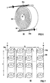
- ein aus dem Supraleiteraufbau erstelltes modulartiges Strombegrenzerelement
- Figur 6
- eine Strombegrenzereinrichtung mit mehreren modulartigen Strombegrenzerelementen nach Figur 5.
Claims (16)
- Supraleiteraufbau zur Führung eines elektrischen Stromes in einer vorbestimmten Richtung mit wenigstens folgenden Teilen:sowieeinem Träger aus metallischen Material,dadurch gekennzeichnet, daß zwischen der Supraleitungsschicht (13, 23, 33) der Leiterbahn (L, L') und dem Träger (11) wenigstens ein der Leiterbahn zugeordneter, sich in Stromführungsrichtung erstreckender, elektrisch leitender Verbindungsteil der Leiterbahn ausgebildet ist, mit dem die Supraleitungsschicht mit dem Träger elektrisch parallelgeschaltet ist.einer auf dem Träger befindlichen Leiterbahn, die zumindestundwenigstens eine auf dem Träger abgeschiedene Zwischenschicht aus elektrisch isolierendem Materialwenigstens eine auf der Zwischenschicht abgeschiedene Supraleitungsschicht aus einem Hoch-Tc-Supraleitermaterial enthält,
- Aufbau nach Anspruch 1, dadurch gekennzeichnet, daß als der mindestens eine Verbindungsteil eine streifenförmige Metallschicht (15a, 15b) vorgesehen ist, die sich seitlich von der Supraleitungsschicht (13) zu einem Randbereich (11a, 11b) des Trägers (11) erstreckt.
- Aufbau nach Anspruch 1, dadurch gekennzeichnet, daß als der mindestens eine Verbindungsteil ein die Zwischenschicht (22, 32) seitlich überlappender Randstreifen (23a, 23b) der Supraleitungsschicht (23) vorgesehen ist, der auf einem entsprechenden Randbereich (11a, 11b) des Trägers (11) aufliegt.
- Aufbau nach Anspruch 3, dadurch gekennzeichnet, daß die Zwischenschicht (32) mit seitlichen Ausnehmungen (35) versehen ist, in denen die Supraleitungsschicht (33) auf dem Träger (11) aufliegt.
- Aufbau nach einem der vorangehenden Ansprüche, gekennzeichnet durch einen Träger (11) aus Cu, Al oder Ag oder deren Legierungen oder aus einem Stahl, insbesondere aus einer NiMo-Legierung.
- Aufbau nach einem der vorangehenden Ansprüche, gekennzeichnet durch mindestens eine Zwischenschicht (12, 22, 32) mit einer an die kristallinen Abmessungen des Supraleitermaterials angepaßter Textur.
- Aufbau nach Anspruch 6, gekennzeichnet durch mindestens eine Zwischenschicht (12, 22, 32) aus biaxial texturiertem, mit Yttrium-stabilisiertem ZrO2 oder CeO2.
- Aufbau nach einem der vorangehenden Ansprüche, gekennzeichnet durch mehrere diskrete Leiterbahnen (L, L') auf einem gemeinsamen Träger (11).
- Verfahren zur Herstellung eines Supraleiteraufbaus nach einem der vorangehenden Ansprüche, dadurch gekennzeichnet, daß zur Ausbildung des wenigstens einen Verbindungsteils zwischen der Supraleitungsschicht (13, 23, 33) und dem Träger (11) in dem mindestens einen Verbindungsbereich eine Abscheidung der Zwischenschicht vermieden oder die Zwischenschicht vor der Abscheidung der Supraleitungsschicht entfernt wird.
- Verfahren zur Herstellung eines Supraleitungsaufbaus nach einem der Ansprüche 1 bis 8, dadurch gekennzeichnet, daß zur Ausbildung des mindestens einen Verbindungsteils zwischen der Supraleitungsschicht (13) und dem Träger (11) wenigstens eine sich über den Verbindungsbereich erstreckende streifenförmige Metallschicht (15a, 15b) abgeschieden wird.
- Verfahren nach Anspruch 9 oder 10, dadurch gekennzeichnet, daß als Abscheideverfahren für das Supraleitermaterial ein gleichzeitiges thermisches Verdampfen der einzelnen Komponenten des Supraleitermaterials unter Sauerstoffzufuhr, oder ein Laserablationsverfahren, oder ein Sputterverfahren oder ein chemisches Verdampfungsverfahren, insbesondere mit metallorganischen Komponenten des Supraleitermaterials, oder ein Siebdruckverfahren vorgesehen wird.
- Verfahren nach einem der Ansprüche 9 bis 11, dadurch gekennzeichnet, daß zur Abscheidung des Zwischenschichtmaterials ein Abscheideverfahren mit Ionenstrom-Unterstützung (IBAD) oder ein Sputterverfahren oder ein Laserablationsverfahren vorgesehen wird.
- Strombegrenzereinrichtung, gekennzeichnet durch mindestens einen Supraleiteraufbau (10, 20, 30) nach einem der Ansprüche 1 bis 8.
- Strombegrenzereinrichtung nach Anspruch 13, gekennzeichnet durch eine elektrische Zusammenschaltung mehrerer modulartiger Strombegrenzerelemente (50i), die jeweils einen Supraleiteraufbau nach einem der Ansprüche 1 bis 8 aufweisen.
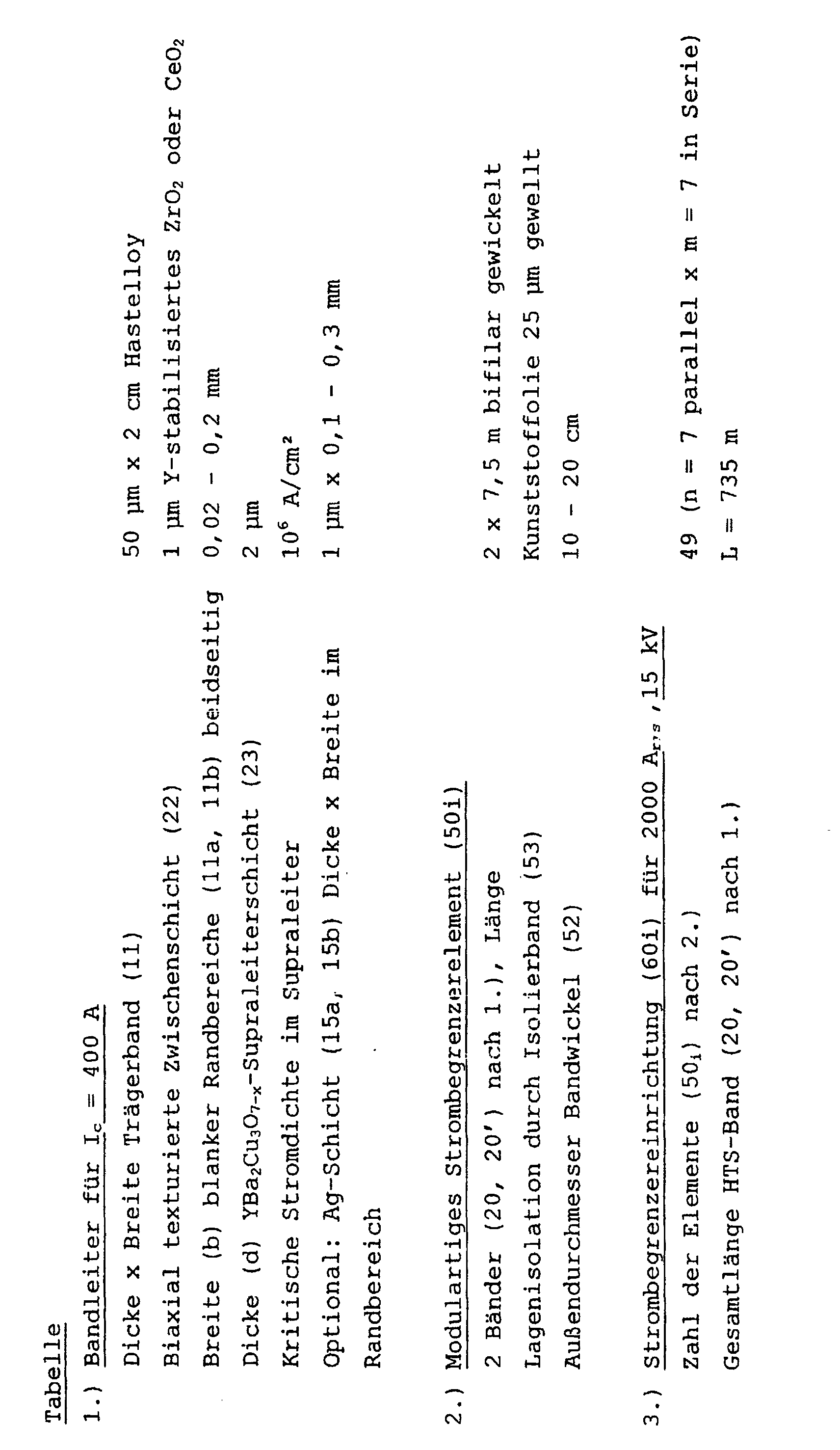
- Strombegrenzereinrichtung nach Anspruch 14, dadurch gekennzeichnet, daß jedes Strombegrenzerelement (50i) einen Wickel (52) aus bifilar gewikkeltem Leiterband (20, 20') mit dem Supraleiteraufbau aufweist.
- Strombegrenzereinrichtung nach Anspruch 15, gekennzeichnet durch Bandleiterwickel (52) mit den Zutritt eines Kühlmittels erleichternden Isolierbändern (53) zwischen benachbarten Leiterbandlagen.
Applications Claiming Priority (3)
| Application Number | Priority Date | Filing Date | Title |
|---|---|---|---|
| DE19756854 | 1997-12-19 | ||
| DE19756854 | 1997-12-19 | ||
| PCT/DE1998/003596 WO1999033122A1 (de) | 1997-12-19 | 1998-12-07 | SUPRALEITERAUFBAU MIT HOCH-Tc-SUPRALEITERMATERIAL, VERFAHREN ZUR HERSTELLUNG DES AUFBAUS SOWIE STROMBEGRENZEREINRICHTUNG MIT EINEM SOLCHEN AUFBAU |
Publications (2)
| Publication Number | Publication Date |
|---|---|
| EP1042820A1 EP1042820A1 (de) | 2000-10-11 |
| EP1042820B1 true EP1042820B1 (de) | 2003-03-12 |
Family
ID=7852730
Family Applications (1)
| Application Number | Title | Priority Date | Filing Date |
|---|---|---|---|
| EP98965108A Expired - Lifetime EP1042820B1 (de) | 1997-12-19 | 1998-12-07 | SUPRALEITERAUFBAU MIT HOCH-T c?-SUPRALEITERMATERIAL, VERFAHREN ZUR HERSTELLUNG DES AUFBAUS SOWIE STROMBEGRENZEREINRICHTUNG MIT EINEM SOLCHEN AUFBAU |
Country Status (8)
| Country | Link |
|---|---|
| US (1) | US6522236B1 (de) |
| EP (1) | EP1042820B1 (de) |
| JP (1) | JP4359387B2 (de) |
| CA (1) | CA2315081A1 (de) |
| DE (1) | DE59807505D1 (de) |
| DK (1) | DK1042820T3 (de) |
| NO (1) | NO20003156L (de) |
| WO (1) | WO1999033122A1 (de) |
Cited By (3)
| Publication number | Priority date | Publication date | Assignee | Title |
|---|---|---|---|---|
| EP2472618A1 (de) | 2011-01-03 | 2012-07-04 | Nexans | Supraleitender ohmischer Fehlerstrombegrenzer |
| EP2991126A1 (de) | 2014-08-25 | 2016-03-02 | Theva Dünnschichttechnik GmbH | Verfahren und Vorrichtung zum Herstellen eines Hochtemperatur-Supraleiters |
| DE102016206573A1 (de) * | 2016-04-19 | 2017-10-19 | Siemens Aktiengesellschaft | Elektrische Spulenwicklung |
Families Citing this family (24)
| Publication number | Priority date | Publication date | Assignee | Title |
|---|---|---|---|---|
| DE19957981A1 (de) * | 1999-12-02 | 2001-06-07 | Abb Research Ltd | Hochtemperatursupraleiteranordnung und Verfahren zu deren Herstellung |
| DE10163008C5 (de) * | 2001-02-07 | 2013-04-18 | Siemens Aktiengesellschaft | Resistive Strombegrenzungseinrichtung mit mindestens einer Leiterbahn mit supraleitendem und normalleitendem Material |
| DE10134515B4 (de) * | 2001-07-16 | 2004-05-06 | W.E.T. Automotive Systems Ag | Leitereinrichtung mit einem eine Verengung aufweisenden flächigen Hauptleiter |
| DE10225935C5 (de) * | 2002-06-11 | 2011-10-06 | THEVA DüNNSCHICHTTECHNIK GMBH | Vorrichtung zum Leiten von Strom |
| DE10230083B3 (de) * | 2002-06-27 | 2004-02-05 | Siemens Ag | Strombegrenzungseinrichtung mit verbesserter Wärmeableitung |
| GB0411035D0 (en) * | 2004-05-18 | 2004-06-23 | Diboride Conductors Ltd | Croygen-free dry superconducting fault current limiter |
| US8088713B2 (en) * | 2004-06-24 | 2012-01-03 | National Institute Of Advanced Industrial Science And Technology | Superconducting fault-current limiting element and the process for producing the same |
| US7816303B2 (en) * | 2004-10-01 | 2010-10-19 | American Superconductor Corporation | Architecture for high temperature superconductor wire |
| DE102004048646B4 (de) | 2004-10-04 | 2006-08-10 | Siemens Ag | Supraleitende Strombegrenzereinrichtung vom resistiven Typ mit bandförmiger Hoch-Tc-Supraleiterbahn |
| DE102004048647B4 (de) | 2004-10-04 | 2006-08-10 | Siemens Ag | Resistive Strombegrenzereinrichtung mit bandförmiger Hoch-Tc-Supraleiterbahn |
| DE102004048648B4 (de) * | 2004-10-04 | 2006-08-10 | Siemens Ag | Vorrichtung zur Strombegrenzung vom resistiven Typ mit bandfömigem Hoch-Tc-Supraleiter |
| DE102004048644B4 (de) * | 2004-10-04 | 2006-08-10 | Siemens Ag | Vorrichtung zur resistiven Strombegrenzung mit bandförmiger Hoch-Tc -Supraleiterbahn |
| RU2414769C2 (ru) * | 2005-07-29 | 2011-03-20 | Американ Суперкондактор Корпорейшн | Сверхпроводящий провод |
| ATE435504T1 (de) | 2006-03-02 | 2009-07-15 | Theva Duennschichttechnik Gmbh | Resistiver strombegrenzer |
| JP4810268B2 (ja) * | 2006-03-28 | 2011-11-09 | 株式会社東芝 | 超電導線材の接続方法及び超電導線材 |
| DE102006032702B3 (de) * | 2006-07-14 | 2007-10-04 | Siemens Ag | Resistive supraleitende Strombegrenzeinrichtung mit bifilarer Spulenwicklung aus HTS-Bandleitern und Windungsabstandshalter |
| DE102006032972B3 (de) * | 2006-07-17 | 2008-02-14 | Siemens Ag | Supraleitende Strombegrenzereinrichtung vom resistiven Typ mit mehrteiligem Halteelement |
| DE102006032973B3 (de) * | 2006-07-17 | 2008-02-14 | Siemens Ag | Supraleitende Strombegrenzereinrichtung von resistiven Typ mit Halteelement |
| DE102008029722B3 (de) * | 2008-06-23 | 2009-12-17 | Siemens Aktiengesellschaft | Leiteranordnung für ein resistives Schaltelement mit wenigstens zwei Leiterverbünden aus supraleitenden Leiterbändern |
| EP2302710B1 (de) * | 2008-11-29 | 2013-01-16 | Alstom Technology Ltd. | Fehlerstrombegrenzer mit mehreren supraleitenden Elementen mit mindestens einem Element mit einem elektrischen Kontakt zwischen dessen supraleitender Schicht und dessen elektrisch leitfähigem Substrat |
| JP5513154B2 (ja) * | 2010-02-12 | 2014-06-04 | 昭和電線ケーブルシステム株式会社 | 酸化物超電導線材及び酸化物超電導線材の製造方法 |
| JP2012256508A (ja) * | 2011-06-08 | 2012-12-27 | Sumitomo Electric Ind Ltd | 超電導線材、および超電導ケーブル |
| JP2016152301A (ja) * | 2015-02-17 | 2016-08-22 | ローム株式会社 | チップ抵抗器およびその製造方法 |
| EP3121860B1 (de) | 2015-07-21 | 2020-11-25 | Nexans | Anordnung zur strombegrenzung in einem der stromversorgung dienenden netzwerk |
Family Cites Families (14)
| Publication number | Priority date | Publication date | Assignee | Title |
|---|---|---|---|---|
| US3098967A (en) * | 1959-01-09 | 1963-07-23 | Sylvania Electric Prod | Cryotron type switching device |
| US3296459A (en) * | 1964-01-13 | 1967-01-03 | Gen Electric | Superconductor circuit with protuberances |
| US3363211A (en) * | 1965-04-02 | 1968-01-09 | Ford Motor Co | Quantum interference device |
| US3936677A (en) * | 1975-01-21 | 1976-02-03 | Bell Telephone Laboratories, Incorporated | Supercurrent device for controlling mobile flux vortices |
| CA1326976C (en) * | 1987-05-26 | 1994-02-15 | Satoshi Takano | Superconducting member |
| SE461306B (sv) * | 1988-06-10 | 1990-01-29 | Asea Brown Boveri | Stroembegraensare |
| US5140300A (en) * | 1988-10-24 | 1992-08-18 | Sharp Kabushiki Kaisha | Superconductive magneto-resistive device comprising laminated superconductive ceramic films |
| JPH02281765A (ja) * | 1989-04-24 | 1990-11-19 | Furukawa Electric Co Ltd:The | 酸化物超電導体薄膜を用いた超電導素子 |
| US5010300A (en) * | 1989-08-11 | 1991-04-23 | Picker International, Inc. | Multi-axis pre-saturated spin echo phase encoded spectroscopy |
| DE4004908A1 (de) | 1990-02-16 | 1991-08-22 | Daimler Benz Ag | Oxidkeramische streifenleiter auf metallischen baendern |
| DE4107685A1 (de) | 1991-03-09 | 1992-09-10 | Abb Patent Gmbh | Supraleitender strombegrenzer |
| DE4119984A1 (de) * | 1991-06-18 | 1992-12-24 | Hoechst Ag | Resistiver strombegrenzer |
| JPH05163005A (ja) * | 1991-12-12 | 1993-06-29 | Mitsubishi Electric Corp | 酸化物超電導限流導体の製造方法 |
| DE19520205A1 (de) | 1995-06-01 | 1996-12-05 | Siemens Ag | Resistive Strombegrenzungseinrichtung unter Verwendung von Hoch-T¶c¶Supraleitermaterial |
-
1998
- 1998-12-07 DE DE59807505T patent/DE59807505D1/de not_active Expired - Lifetime
- 1998-12-07 JP JP2000525935A patent/JP4359387B2/ja not_active Expired - Lifetime
- 1998-12-07 DK DK98965108T patent/DK1042820T3/da active
- 1998-12-07 WO PCT/DE1998/003596 patent/WO1999033122A1/de active IP Right Grant
- 1998-12-07 EP EP98965108A patent/EP1042820B1/de not_active Expired - Lifetime
- 1998-12-07 CA CA002315081A patent/CA2315081A1/en not_active Abandoned
-
2000
- 2000-06-13 US US09/592,743 patent/US6522236B1/en not_active Expired - Lifetime
- 2000-06-16 NO NO20003156A patent/NO20003156L/no not_active Application Discontinuation
Cited By (3)
| Publication number | Priority date | Publication date | Assignee | Title |
|---|---|---|---|---|
| EP2472618A1 (de) | 2011-01-03 | 2012-07-04 | Nexans | Supraleitender ohmischer Fehlerstrombegrenzer |
| EP2991126A1 (de) | 2014-08-25 | 2016-03-02 | Theva Dünnschichttechnik GmbH | Verfahren und Vorrichtung zum Herstellen eines Hochtemperatur-Supraleiters |
| DE102016206573A1 (de) * | 2016-04-19 | 2017-10-19 | Siemens Aktiengesellschaft | Elektrische Spulenwicklung |
Also Published As
| Publication number | Publication date |
|---|---|
| EP1042820A1 (de) | 2000-10-11 |
| CA2315081A1 (en) | 1999-07-01 |
| DE59807505D1 (de) | 2003-04-17 |
| JP2001527298A (ja) | 2001-12-25 |
| DK1042820T3 (da) | 2003-07-14 |
| NO20003156D0 (no) | 2000-06-16 |
| JP4359387B2 (ja) | 2009-11-04 |
| WO1999033122A1 (de) | 1999-07-01 |
| US6522236B1 (en) | 2003-02-18 |
| NO20003156L (no) | 2000-06-16 |
Similar Documents
| Publication | Publication Date | Title |
|---|---|---|
| EP1042820B1 (de) | SUPRALEITERAUFBAU MIT HOCH-T c?-SUPRALEITERMATERIAL, VERFAHREN ZUR HERSTELLUNG DES AUFBAUS SOWIE STROMBEGRENZEREINRICHTUNG MIT EINEM SOLCHEN AUFBAU | |
| EP1797599B1 (de) | Supraleitende strombegrenzereinrichtung vom resistiven typ mit bandförmiger hoch-tc-supraleiterbahn | |
| EP2041809B1 (de) | Resistive supraleitende strombegrenzereinrichtung mit bifilarer spulenwicklung aus hts-bandleitern und windungsabstandshalter | |
| EP0829101B1 (de) | RESISTIVE STROMBEGRENZUNGSEINRICHTUNG UNTER VERWENDUNG VON HOCH-Tc-SUPRALEITERMATERIAL | |
| EP1088351B1 (de) | STROMBEGRENZUNGSEINRICHTUNG MIT LEITERBAHNANORDNUNG AUS HOCH-Tc-SUPRALEITERMATERIAL SOWIE VERFAHREN ZUR HERSTELLUNG DER EINRICHTUNG | |
| EP1508175B1 (de) | VERFAHREN ZUR HERSTELLUNG EINES VOLLTRANSPONIERTEN HOCH-Tc-VERBUNDSUPRALEITERS SOWIE NACH DEM VERFAHREN HERGESTELLTER LEITER | |
| EP1105924B1 (de) | Resistiver kurzschlussstrombegrenzer mit einer leiterbahnstruktur aus hochtemperatur-supraleitermaterial sowie verfahren zur herstellung des strombegrenzers | |
| EP1797601B1 (de) | VORRICHTUNG ZUR RESISTIVEN STROMBEGRENZUNG MIT BANDFÖRMIGER HOCH-Tc-SUPRALEITERBAHN | |
| EP2830107B1 (de) | Bandförmiges, supraleitendes Element mit verbessertem Eigenschutz im Quenchfall | |
| EP1797600B1 (de) | VORRICHTUNG ZUR STROMBEGRENZUNG VOM RESISTIVEN TYP MIT BANDFÖRMIGEM HOCH-Tc-SUPRALEITER | |
| DE10225935C5 (de) | Vorrichtung zum Leiten von Strom | |
| DE19832273C1 (de) | Resistiver Strombegrenzer mit Hoch-T¶c¶-Supraleitermaterial sowie Verfahren zur Herstellung des Strombegrenzers | |
| DE102004048647B4 (de) | Resistive Strombegrenzereinrichtung mit bandförmiger Hoch-Tc-Supraleiterbahn | |
| EP0405677B1 (de) | Supraleitendes elektronisches Dünnschichtbauelement und Verfahren zu seiner Herstellung | |
| DE3815183C2 (de) | ||
| DE4128224C2 (de) | Einrichtung zum Verbinden eines Normalleiterstückes mit einem Hochtemperatursupraleiterstück | |
| DE10226391A1 (de) | Resistiver Strombegrenzer wenigstens einer supraleitenden Leiterbahn | |
| DE19827223C5 (de) | Resistiver Strombegrenzer mit Hoch-Tc-Supraleitermaterial und Verfahren zu dessen Herstellung | |
| DE19906298A1 (de) | Bandförmiger Multifilamentsupraleiter mit Bi-Cuprat-Filamenten | |
| EP0809305A1 (de) | Bandförmiger Hoch-Tc-Multi-Filamentsupraleiter und Verfahren zu dessen Herstellung |
Legal Events
| Date | Code | Title | Description |
|---|---|---|---|
| PUAI | Public reference made under article 153(3) epc to a published international application that has entered the european phase |
Free format text: ORIGINAL CODE: 0009012 |
|
| 17P | Request for examination filed |
Effective date: 20000417 |
|
| AK | Designated contracting states |
Kind code of ref document: A1 Designated state(s): CH DE DK FR GB IT LI NL SE |
|
| GRAH | Despatch of communication of intention to grant a patent |
Free format text: ORIGINAL CODE: EPIDOS IGRA |
|
| GRAH | Despatch of communication of intention to grant a patent |
Free format text: ORIGINAL CODE: EPIDOS IGRA |
|
| GRAA | (expected) grant |
Free format text: ORIGINAL CODE: 0009210 |
|
| AK | Designated contracting states |
Designated state(s): CH DE DK FR GB IT LI NL SE |
|
| REG | Reference to a national code |
Ref country code: GB Ref legal event code: FG4D Free format text: NOT ENGLISH |
|
| REG | Reference to a national code |
Ref country code: CH Ref legal event code: EP |
|
| REF | Corresponds to: |
Ref document number: 59807505 Country of ref document: DE Date of ref document: 20030417 Kind code of ref document: P |
|
| REG | Reference to a national code |
Ref country code: CH Ref legal event code: NV Representative=s name: SIEMENS SCHWEIZ AG |
|
| REG | Reference to a national code |
Ref country code: SE Ref legal event code: TRGR |
|
| REG | Reference to a national code |
Ref country code: DK Ref legal event code: T3 |
|
| GBT | Gb: translation of ep patent filed (gb section 77(6)(a)/1977) |
Effective date: 20030723 |
|
| ET | Fr: translation filed | ||
| PLBE | No opposition filed within time limit |
Free format text: ORIGINAL CODE: 0009261 |
|
| STAA | Information on the status of an ep patent application or granted ep patent |
Free format text: STATUS: NO OPPOSITION FILED WITHIN TIME LIMIT |
|
| 26N | No opposition filed |
Effective date: 20031215 |
|
| PGFP | Annual fee paid to national office [announced via postgrant information from national office to epo] |
Ref country code: GB Payment date: 20041207 Year of fee payment: 7 |
|
| PGFP | Annual fee paid to national office [announced via postgrant information from national office to epo] |
Ref country code: DK Payment date: 20041208 Year of fee payment: 7 |
|
| PGFP | Annual fee paid to national office [announced via postgrant information from national office to epo] |
Ref country code: CH Payment date: 20050304 Year of fee payment: 7 |
|
| PG25 | Lapsed in a contracting state [announced via postgrant information from national office to epo] |
Ref country code: GB Free format text: LAPSE BECAUSE OF NON-PAYMENT OF DUE FEES Effective date: 20051207 |
|
| PG25 | Lapsed in a contracting state [announced via postgrant information from national office to epo] |
Ref country code: LI Free format text: LAPSE BECAUSE OF NON-PAYMENT OF DUE FEES Effective date: 20051231 Ref country code: CH Free format text: LAPSE BECAUSE OF NON-PAYMENT OF DUE FEES Effective date: 20051231 |
|
| PG25 | Lapsed in a contracting state [announced via postgrant information from national office to epo] |
Ref country code: DK Free format text: LAPSE BECAUSE OF NON-PAYMENT OF DUE FEES Effective date: 20060102 |
|
| REG | Reference to a national code |
Ref country code: DK Ref legal event code: EBP |
|
| REG | Reference to a national code |
Ref country code: CH Ref legal event code: PL |
|
| GBPC | Gb: european patent ceased through non-payment of renewal fee |
Effective date: 20051207 |
|
| REG | Reference to a national code |
Ref country code: FR Ref legal event code: PLFP Year of fee payment: 18 |
|
| REG | Reference to a national code |
Ref country code: FR Ref legal event code: PLFP Year of fee payment: 19 |
|
| REG | Reference to a national code |
Ref country code: FR Ref legal event code: PLFP Year of fee payment: 20 |
|
| PGFP | Annual fee paid to national office [announced via postgrant information from national office to epo] |
Ref country code: FR Payment date: 20171214 Year of fee payment: 20 Ref country code: NL Payment date: 20171213 Year of fee payment: 20 |
|
| PGFP | Annual fee paid to national office [announced via postgrant information from national office to epo] |
Ref country code: SE Payment date: 20171211 Year of fee payment: 20 |
|
| PGFP | Annual fee paid to national office [announced via postgrant information from national office to epo] |
Ref country code: DE Payment date: 20180219 Year of fee payment: 20 |
|
| PGFP | Annual fee paid to national office [announced via postgrant information from national office to epo] |
Ref country code: IT Payment date: 20171221 Year of fee payment: 20 |
|
| REG | Reference to a national code |
Ref country code: DE Ref legal event code: R071 Ref document number: 59807505 Country of ref document: DE |
|
| REG | Reference to a national code |
Ref country code: NL Ref legal event code: MK Effective date: 20181206 |
|
| REG | Reference to a national code |
Ref country code: SE Ref legal event code: EUG |