EP1041867A2 - Printed circuit board and manufacturing method of the printed circuit board - Google Patents
Printed circuit board and manufacturing method of the printed circuit board Download PDFInfo
- Publication number
- EP1041867A2 EP1041867A2 EP00302344A EP00302344A EP1041867A2 EP 1041867 A2 EP1041867 A2 EP 1041867A2 EP 00302344 A EP00302344 A EP 00302344A EP 00302344 A EP00302344 A EP 00302344A EP 1041867 A2 EP1041867 A2 EP 1041867A2
- Authority
- EP
- European Patent Office
- Prior art keywords
- insulative layer
- circuit pattern
- circuit board
- printed circuit
- insulative
- Prior art date
- Legal status (The legal status is an assumption and is not a legal conclusion. Google has not performed a legal analysis and makes no representation as to the accuracy of the status listed.)
- Withdrawn
Links
- 238000004519 manufacturing process Methods 0.000 title claims abstract description 27
- 238000000034 method Methods 0.000 claims abstract description 81
- 238000009713 electroplating Methods 0.000 claims abstract description 36
- 238000001312 dry etching Methods 0.000 claims abstract description 33
- 239000011347 resin Substances 0.000 claims abstract description 30
- 229920005989 resin Polymers 0.000 claims abstract description 30
- 239000000463 material Substances 0.000 claims abstract description 16
- 239000000758 substrate Substances 0.000 claims abstract description 16
- 238000005530 etching Methods 0.000 claims abstract description 13
- XKRFYHLGVUSROY-UHFFFAOYSA-N Argon Chemical compound [Ar] XKRFYHLGVUSROY-UHFFFAOYSA-N 0.000 claims description 4
- 239000011261 inert gas Substances 0.000 claims description 3
- 229910052786 argon Inorganic materials 0.000 claims description 2
- 239000002131 composite material Substances 0.000 abstract description 5
- 239000010949 copper Substances 0.000 description 16
- RYGMFSIKBFXOCR-UHFFFAOYSA-N Copper Chemical compound [Cu] RYGMFSIKBFXOCR-UHFFFAOYSA-N 0.000 description 15
- 229910052802 copper Inorganic materials 0.000 description 14
- CURLTUGMZLYLDI-UHFFFAOYSA-N Carbon dioxide Chemical compound O=C=O CURLTUGMZLYLDI-UHFFFAOYSA-N 0.000 description 12
- 239000003822 epoxy resin Substances 0.000 description 9
- 229920000647 polyepoxide Polymers 0.000 description 9
- PXHVJJICTQNCMI-UHFFFAOYSA-N nickel Substances [Ni] PXHVJJICTQNCMI-UHFFFAOYSA-N 0.000 description 7
- 229910002092 carbon dioxide Inorganic materials 0.000 description 6
- 239000001569 carbon dioxide Substances 0.000 description 6
- 239000011162 core material Substances 0.000 description 6
- 239000000945 filler Substances 0.000 description 6
- 239000000956 alloy Substances 0.000 description 5
- 229910045601 alloy Inorganic materials 0.000 description 5
- JNDMLEXHDPKVFC-UHFFFAOYSA-N aluminum;oxygen(2-);yttrium(3+) Chemical compound [O-2].[O-2].[O-2].[Al+3].[Y+3] JNDMLEXHDPKVFC-UHFFFAOYSA-N 0.000 description 5
- XEEYBQQBJWHFJM-UHFFFAOYSA-N iron Substances [Fe] XEEYBQQBJWHFJM-UHFFFAOYSA-N 0.000 description 5
- 229910019901 yttrium aluminum garnet Inorganic materials 0.000 description 5
- 239000007789 gas Substances 0.000 description 4
- 239000012286 potassium permanganate Substances 0.000 description 4
- 238000010521 absorption reaction Methods 0.000 description 3
- 239000003054 catalyst Substances 0.000 description 3
- 239000011889 copper foil Substances 0.000 description 3
- 239000000203 mixture Substances 0.000 description 3
- KDLHZDBZIXYQEI-UHFFFAOYSA-N Palladium Chemical compound [Pd] KDLHZDBZIXYQEI-UHFFFAOYSA-N 0.000 description 2
- 229910052742 iron Inorganic materials 0.000 description 2
- 239000007788 liquid Substances 0.000 description 2
- 229910052759 nickel Inorganic materials 0.000 description 2
- 238000000059 patterning Methods 0.000 description 2
- 238000001020 plasma etching Methods 0.000 description 2
- 238000007650 screen-printing Methods 0.000 description 2
- 238000005406 washing Methods 0.000 description 2
- 244000025254 Cannabis sativa Species 0.000 description 1
- 238000005299 abrasion Methods 0.000 description 1
- 238000004380 ashing Methods 0.000 description 1
- 238000000576 coating method Methods 0.000 description 1
- 239000004020 conductor Substances 0.000 description 1
- 230000003247 decreasing effect Effects 0.000 description 1
- 230000001066 destructive effect Effects 0.000 description 1
- 230000002500 effect on skin Effects 0.000 description 1
- 230000000694 effects Effects 0.000 description 1
- 238000001704 evaporation Methods 0.000 description 1
- -1 for example Polymers 0.000 description 1
- 239000011521 glass Substances 0.000 description 1
- 239000011256 inorganic filler Substances 0.000 description 1
- 238000009413 insulation Methods 0.000 description 1
- 238000007733 ion plating Methods 0.000 description 1
- 150000002500 ions Chemical class 0.000 description 1
- 230000001678 irradiating effect Effects 0.000 description 1
- 239000002075 main ingredient Substances 0.000 description 1
- 239000000155 melt Substances 0.000 description 1
- 229910052751 metal Inorganic materials 0.000 description 1
- 239000002184 metal Substances 0.000 description 1
- 238000012986 modification Methods 0.000 description 1
- 230000004048 modification Effects 0.000 description 1
- 230000003472 neutralizing effect Effects 0.000 description 1
- 239000012766 organic filler Substances 0.000 description 1
- 238000004806 packaging method and process Methods 0.000 description 1
- 238000012856 packing Methods 0.000 description 1
- 229910052763 palladium Inorganic materials 0.000 description 1
- 239000002245 particle Substances 0.000 description 1
- 238000007747 plating Methods 0.000 description 1
- 229920001721 polyimide Polymers 0.000 description 1
- 239000009719 polyimide resin Substances 0.000 description 1
- 238000004544 sputter deposition Methods 0.000 description 1
- 239000000126 substance Substances 0.000 description 1
Images


Classifications
-
- H—ELECTRICITY
- H05—ELECTRIC TECHNIQUES NOT OTHERWISE PROVIDED FOR
- H05K—PRINTED CIRCUITS; CASINGS OR CONSTRUCTIONAL DETAILS OF ELECTRIC APPARATUS; MANUFACTURE OF ASSEMBLAGES OF ELECTRICAL COMPONENTS
- H05K3/00—Apparatus or processes for manufacturing printed circuits
- H05K3/38—Improvement of the adhesion between the insulating substrate and the metal
- H05K3/381—Improvement of the adhesion between the insulating substrate and the metal by special treatment of the substrate
-
- H—ELECTRICITY
- H05—ELECTRIC TECHNIQUES NOT OTHERWISE PROVIDED FOR
- H05K—PRINTED CIRCUITS; CASINGS OR CONSTRUCTIONAL DETAILS OF ELECTRIC APPARATUS; MANUFACTURE OF ASSEMBLAGES OF ELECTRICAL COMPONENTS
- H05K3/00—Apparatus or processes for manufacturing printed circuits
- H05K3/38—Improvement of the adhesion between the insulating substrate and the metal
- H05K3/388—Improvement of the adhesion between the insulating substrate and the metal by the use of a metallic or inorganic thin film adhesion layer
-
- H—ELECTRICITY
- H05—ELECTRIC TECHNIQUES NOT OTHERWISE PROVIDED FOR
- H05K—PRINTED CIRCUITS; CASINGS OR CONSTRUCTIONAL DETAILS OF ELECTRIC APPARATUS; MANUFACTURE OF ASSEMBLAGES OF ELECTRICAL COMPONENTS
- H05K3/00—Apparatus or processes for manufacturing printed circuits
- H05K3/46—Manufacturing multilayer circuits
- H05K3/4644—Manufacturing multilayer circuits by building the multilayer layer by layer, i.e. build-up multilayer circuits
Definitions
- the present invention relates to a multi-layer printed circuit board such as a build-up printed circuit board mounted with an electronic component part such as a bare chip, and relates to a manufacturing method of the printed circuit board.
- a printed circuit board is utilized for mounting a circuit element such as various kind of electronic component parts in an electronic apparatus.
- a printed circuit board is demanded to reduce its dimensions and a circuit pattern is demanded to be finer in accordance with requirements for an electronic apparatus and a circuit element to minimize their dimensions and to integrate them in a high packing density.
- a line width of a circuit pattern and a line pitch between adjoining circuit patterns on a printed circuit board are respectively some 75 ⁇ m.
- a finer pattern is demanded for mounting a bare chip directly on a printed circuit board or for packaging a bare chip by utilizing a printed circuit board. Accordingly such line width and line pitch are demanded to be smaller than 40 ⁇ m.
- Figs. 4(a) through 4(h) show each step of manufacturing method of a printed circuit board in accordance with the prior art.
- a metal film such as a copper foil is formed over a core material 1 as an insulative base substrate composed of glass epoxy resin or like.
- the copper foil is patterned and formed as a first circuit pattern 2.
- a line width L1 and a line pitch L2 of the first circuit pattern 2 are some 75 ⁇ m minimum and its thickness W1 is some 20 ⁇ m.
- a blacking treatment is applied to a surface of the first circuit pattern 2 so as to increase a degree of contact with an insulative layer composed of epoxy resin, which is formed over the surface of the first circuit pattern 2 in a succeeding process.
- an insulative layer 3 is formed all aver the surface of the core material 1 by using such a method as a screen-printing.
- a main ingredient of the insulative layer 3 is epoxy resin.
- An appropriate amount of inorganic or organic filler 4 of which particle diameter is approximately 10 ⁇ m is mixed in the epoxy resin of the insulative layer 3 and the filler 4 is dissolved during a roughing process, which will be depicted.
- a thickness of the insulative layer 3 is designed to be 40 to 70 ⁇ m.
- a carbon dioxide laser beam 5 irradiates the insulative layer 3 so as to perforate a hole 6 for connection selectively at a predetermined location and to expose the first circuit pattern 2.
- a residue 7 can remain on the surface of the first circuit pattern 2 while perforating the hole 6 by the carbon dioxide laser beam 5.
- a diameter of the hole 6 is some 100 ⁇ m.
- Fig. 4(d) by applying alkalescent roughing medicinal solution such as potassium permanganate, the surface of the insulative layer 3 is roughed by forming a plurality of pits 8 with dissolving the filler 4, which is solvable by the roughing medicinal solution. Further, the residue 7 remaining in the hole 6 as shown in Fig. 4(c) is cleaned up and removed by an action of the potassium permanganate.
- alkalescent roughing medicinal solution such as potassium permanganate
- a catalyst 9 is adhered to the surface of the insulative layer 4 and the first circuit pattern 2 by applying a solution dissolving tint and palladium, for example, over the surface of the insulative layer 3 and the first circuit pattern 2 so as to increase conductiveness of the surface of all over the insulative layer 3.
- a first conductive film 10 for electroplating of which main component is copper is formed as a foundation all over the surface of the insulative layer 3 by the non-electrolytic plating, wherein a thickness of the first conductive film 10 is accumulated to approximately 0.3 ⁇ m.
- a second conductive film 11 of copper is formed over the first conductive film 10 by the electroplating process, wherein a thickness of the second conductive film 11 is accumulated to approximately 20 ⁇ m. Accordingly, the first circuit pattern 2 can be electrically connected to the second conductive film 11. Further, as shown in Fig. 4(h), a second circuit pattern 12 is obtained by etching the second conductive film 11.
- a third circuit pattern is formed after another insulative layer is formed over the second circuit pattern 11 in a regular manufacturing process.
- a multi-layer printed circuit board can be manufactured by repeating the processes mentioned above.
- the manufacturing method mentioned above is a wet type process of utilizing medicinal solution such as alkalescent potassium permanganate and non-electrolytic plating liquid. Accordingly, further problem occurs such that an additional process of washing off medicinal solution is necessary at each time the medicinal solution is applied and effluent must be processed properly.
- an object of the present invention is to provide a printed circuit board and a manufacturing method of the printed circuit board, which can effectively manufacture a printed circuit board having an extremely small anchor profile and a finer pattern in few manufacturing processes by utilizing a dry etching method and a film forming method by spattering.
- the present invention provides, according to an aspect thereof, a printed circuit board comprising a circuit pattern formed on a surface of a base substrate of which surface is at least composed of an insulative material, an insulative layer formed over the surface of the base substrate including the circuit pattern and composed of a mixed insulative material of more than two kinds of organic resins having a different etching rate by a dry etching process, a hole for connection perforated on the insulative layer by a laser beam or like, a conductive film for electroplating process as a foundation of electroplating formed on the surface of the insulative layer by a vacuum film forming process after roughing the surface of the insulative layer by removing a part of the surface of the insulative layer with a dry etching process and a conductive layer formed over the conductive film by an electroplating process, wherein the conductive layer is connected with the circuit pattern electrically.
- a manufacturing method of a printed circuit board comprising steps of forming a circuit pattern on a surface of a base substrate of which surface is at least composed of an insulative material, forming an insulative layer over the surface of the base substrate including the circuit pattern and the insulative layer composed of a mixed insulative material of more than two kinds of organic resins having a different etching rate by a dry etching process, perforating a hole for connection on the insulative layer by a laser beam or like, roughing the surface of the insulative layer by removing a part of the surface of the insulative layer with a dry etching process, forming a conductive film for electroplating process as a foundation of electroplating on the surface of the insulative layer by a vacuum film forming process and forming a conductive layer over the conductive film by an electroplating process, wherein the conductive layer is connected with the circuit pattern electrically.
- a printed circuit board which is excellent in a radio frequency (RF) characteristic because of having a finer and thinner circuit pattern than a current printed circuit board.
- the printed circuit board comprises a base substrate, a first circuit pattern, an insulative layer, a hole for connection, a conductive film for electroplating and a conductive layer for a second circuit pattern.
- the first circuit pattern is formed on a surface of the base substrate of which the surface is at least made from an insulative material.
- the insulative layer which is made from an insulative material composed of more than two organic resins having a different etching rate for a dry etching process from each other, is formed over the base substrate including the first circuit pattern.
- the hole for connection is perforated on the insulative layer by means of laser beam or like.
- the surface of the insulative layer is roughed by removing a part of it with a dry etching process.
- the conductive film for electroplating is formed over the surface of the insulative layer, which is dry etched, so as to be a foundation for the electroplating.
- the conductive layer is formed by the electroplating process over the conductive film for electroplating.
- the conductive layer is connected electrically with the first circuit pattern.
- the second circuit pattern is formed by etching the conductive layer. Accordingly, the printed circuit board in accordance with a first embodiment of the present invention is provided.
- a printed circuit board which has profiles of a finer line width, a finer line pitch and a finer roughing process, can be provided in a fewer manufacturing processes than the current manufacturing process without increasing a number of processing steps.
- the insulative layer mentioned above is composed of mixed compositions of more than two organic resins having a different dry etching rate from each other and processed through an ion bombard method with inert gas such as Ar (argon), which is applied to the compositions. Accordingly, the insulative layer can be formed with extremely fine and uniform rugged surface in a unit of molecular cluster and an anchor profile of less than 2 ⁇ m can be obtained. The fine and uniform rugged surface can maintain flatness at an interface of resins, which affect linearity and an RF characteristic, for a finer pattern than smaller than 40 ⁇ m, for example. Further, by using such a resin excluding filler, which roughens a surface of the insulative layer too much, a thinner insulative layer can sustain sufficient insulation characteristics. Furthermore, such the insulative layer can make a contribution to thinning a printed circuit board and to lightening its weight.
- Ar argon
- An upper limit of a degree of face roughness is approximately 2 ⁇ m in order to form a pattern as mentioned above. If a degree of face roughness is less than 0.1 ⁇ m, a sufficient contact strength can no be obtained. Thus, a degree of face roughness of an insulative layer is desirable within a range of from 0.1 to 2 ⁇ m.
- the conductive film for electroplating mentioned above is formed by a vacuum film forming method such as sputtering, ion plating and evaporating on the fine rugged surface formed by the dry etching process, the conductive film having a enough contact strength can be formed.
- a material of the conductive film Ni (nickel) and Fe (iron) and their alloy with copper are best because they have affinity with resin and can be easily etched by etching solution for copper.
- a temperature for forming film it is more effective to heat while forming a film, although a contact strength can be obtained sufficiently in the normal temperature. Further, a contact strength can be improved and a total time duration of manufacturing a printed circuit board can be reduced by applying sequentially a dry etching and a vacuum film forming method with keeping a non-destructive vacuum environment.
- a carbon dioxide laser beam is commonly utilized for perforating the hole for connection.
- processing an area of less than 50 ⁇ m is hardly feasible because a wave length of the laser beam is approximately 10 ⁇ m, which is rather long, so that a spot of the laser beam can hardly be focused.
- residue of resin remains in approximately 1 ⁇ m thick after the laser processing, the residue must be removed by such a method as de-smearing.
- a YAG (yttrium aluminum garnet) laser having a wave length of 400 to 600 nm is utilized for perforating the hole for connection, so that resin residue can be eliminated in conjunction with focusing a laser spot in an extremely small diameter.
- an absorption ratio of copper to a laser beam is less than 10 %, so that all most all laser beam are reflected on the surface of the insulative layer and not abrade into the insulative layer. Accordingly, the laser beam generates heat and melts surrounding resin, so that the melted resin remains in film.
- an absorption ration of copper to the YAG laser beam is from 20 to 55 %, copper is abraded properly, so that such the resin residue does not remain. Accordingly, the process of de-smearing is not necessary.
- a wave length of a laser beam is smaller than 400 nm, an absorption ratio of copper increases and the circuit pattern may be perforated as deep as some ⁇ m due to excess abrasion. Therefore, in a case that a thickness of copper becomes thinner in accordance with being a circuit pattern made finer in near future, a laser processing by using the wave length of less than 400 nm is harmful for copper of a circuit pattern because the copper is shaved too thin.
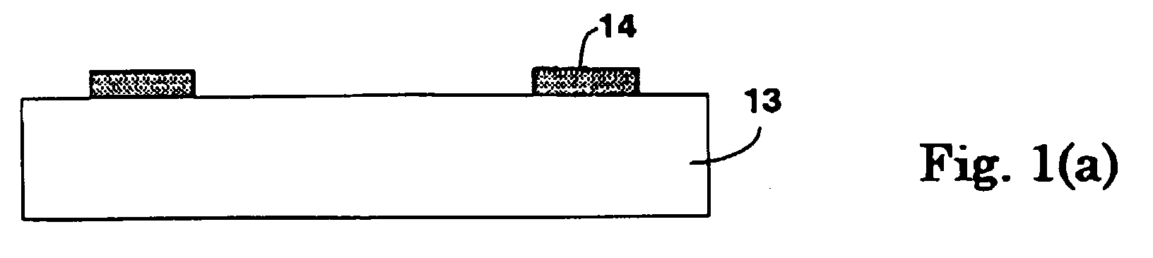
- Figs. 1(a) through 1(g) show each step of manufacturing a printed circuit board according to an embodiment of the present invention.
- a manufacturing method of a printed circuit board which is characterized by that an electroplating process is only adopted as a wet processing and other processes are a dry etching and a vacuum film forming processes.
- a first circuit pattern 14 is formed by patterning copper foil or like built up over a surface of an insulative core material 13, which is composed of grass epoxy resin as a base substrate.
- a surface of the first circuit pattern 14 is oxidized and applied with a blacking treatment.
- an insulative layer 15 is formed all over the core material 13 including the first circuit pattern 14 by a coating process such as a screen printing.
- the insulative layer 15 comprises insulative materials of mixed composites, which are more than two kinds of organic resins having a different dry etching rate from each other.
- Major material of the insulative layer 15 is a mixed composites of an epoxy resin, for example, and a polyimide resin of which dry etching rate is relatively higher than that of the epoxy resin.
- Filler as a roughing composition mentioned above is not included in the insulative layer 15.
- a thickness W2 of the insulative layer 15 is designed to from 20 to 30 ⁇ m. The thickness is more thinner than that of a current printed circuit board, that is, 40 to 70 ⁇ m.
- a hole 17 for connection is selectively perforated through the insulative layer 15 by irradiating a YAG laser beam 16 of a wave length of 400 to 600 nm so as to expose the internal first circuit pattern 14.
- a diameter of the hole 17 is 20 to 50 ⁇ m and is further smaller than that of a current printed circuit board.
- a residue 18 may remain, if a carbon dioxide laser beam is utilized for perforating the hole 17 as mentioned above.
- the total core material including the first circuit pattern 14 and the insulative layer 15 shown in Fig. 1(c) is applied with a dry etching process in a dry etching apparatus. Further details of the dry etching process are depicted with referring Figs. 2 and 3.
- Fig. 2 shows an enlarged plan view of a part "G" shown in Fig. 1(d).
- Fig. 3 shows an enlarged sectional view of the part "G" shown in Fig. 1(d).
- the insulative layer 15 is mixed composites of a first resin 22 having a higher dry etching rate and a second resin 23 having a lower dry etching rate than that of the first resin 22.
- a surface of the first resin 22 is slightly shaved by the dry etching process and removed selectively.
- the second resin 23 having the lower dry etching rate remains with forming a projection 24 because the first resin 23 is hardly removed by the dry etching process.
- a uniform rugged surface appears on the surface of the insulative layer 15. Accordingly, the surface of the insulative layer 15 is roughed uniformly.
- a regular reactive ion etching (RIE) apparatus or an ashing device such as a chemical dry etching (CDE) apparatus can be utilized as an etching apparatus.
- RIE reactive ion etching
- CDE chemical dry etching
- inert gas such as Ar is utilized as etching gas.
- a partial pressure of the gas is 0.03 to 1.0 Torr although it varies by resin to be etched.
- the residue 18 may slightly remain in the hole 17 in a depth of approximately 10 nm while perforating the hole 17 by a carbon dioxide laser beam. However, the residue 18 is removed during the dry etching process, in other words, by a reverse spattering phenomenon.
- the total core material is applied with a spattering film forming process in a spattering apparatus, which applies a vacuum film forming process.
- a conductive film 19 for electroplating is formed all over the insulative layer 15 and an inner wall of the hale 17 until the thickness of the conductive film becomes approximately 0.3 ⁇ m, for example.
- An alloy composed of 90 % of Ni and 10 % of Cu, for example, is utilized for a material of the conductive film 19.
- a direct current (DC) magnetron spattering apparatus for example, can be utilized for a spattering apparatus.
- An Ar gas can be utilized for a plasma gas.
- a conductive layer 20 composed of copper is formed in approximately 20 ⁇ m thick, for example, on the conductive film 19 for electroplating by an electroplating process. Accordingly, the conductive layer 20 can be electrically connected to the first circuit pattern 14 in a lower layer of the printed circuit board.
- a second circuit pattern 21 is formed by etching the conductive layer 20.
- a line width L3 and a line pitch L4 of the second circuit pattern 21 are 20 to 40 ⁇ m respectively. They are much finer than those of a current printed circuit board are.
- a depth W3 of the second circuit pattern 21 is 5 to 15 ⁇ m.
- a surface of the second circuit pattern 21 is oxidized and applied with a blacking treatment so as to increase a degree of contact with an epoxy resin layer, which is built up on the surface of the second circuit pattern 21 in a succeeding process, and then another insulative layer is formed all over the second circuit pattern 21.
- This printed circuit board having another insulative layer is treated as a base substrate and applied with patterning of a circuit pattern once again, and then a multi-layer printed circuit board, that is, a build-up printed circuit board is manufactured by repeating the above mentioned processes.
- the roughing process of a resin surface of an insulative layer and the forming process of a conductive film for electroplating by an non-electrolytic plating method are processed in a dry condition without utilizing liquid although a wet process is applied for a current method, many washing processes and neutralizing processes, which are necessary for the current method by a wet process, can be eliminated.
- the line width L3 and the line pitch L4 of the second circuit pattern 21, the thickness W2 of the insulative layer 15 and the diameter of the hole 17 are not limited to the values mentioned above. Any dimensions are acceptable.
- an anchor profile which assures a degree of contact between a conductive layer and a resin or an insulative layer, can be designated as small as 0.1 to 2.0 ⁇ m. Accordingly, a fine pattern having a line width and a line pitch of 10 to 40 ⁇ m can be formed and the fine pattern improves an RF characteristic in conjunction with fining an anchor.
- a number of resins utilized for the insulative layer 15 is not limited to two. Any number of resins can be utilized as well.
- a printed circuit board and a manufacturing method of the printed circuit board which exhibits following effects.
- a printed circuit board having a fine circuit pattern can be manufactured without increasing a number of manufacturing processes or with decreasing a number of manufacturing processes. Accordingly, a printed circuit board, which is low in price, thin in thickness, excellent in an RF characteristic and has a fine pattern, can be provided.
Landscapes
- Engineering & Computer Science (AREA)
- Manufacturing & Machinery (AREA)
- Microelectronics & Electronic Packaging (AREA)
- Manufacturing Of Printed Wiring (AREA)
- Manufacturing Of Printed Circuit Boards (AREA)
- Printing Elements For Providing Electric Connections Between Printed Circuits (AREA)
- Welding Or Cutting Using Electron Beams (AREA)
- Laser Beam Processing (AREA)
Abstract
Description
Claims (4)
- A printed circuit board comprising:a circuit pattern formed on a surface of a base substrate of which surface is at least composed of an insulative material;an insulative layer formed over the surface of said base substrate including said circuit pattern and composed of a mixed insulative material of more than two kinds of organic resins having a different etching rate by a dry etching process;a hole for connection perforated on said insulative layer by a laser beam or like;a conductive film for electroplating process as a foundation of electroplating formed on the surface of said insulative layer by a vacuum film forming process after roughing the surface of said insulative layer by removing a part of the surface of said insulative layer with a dry etching process; anda conductive layer formed over said conductive film by an electroplating process,
wherein said conductive layer is connected with said circuit pattern electrically. - A manufacturing method of a printed circuit board comprising steps of:forming a circuit pattern on a surface of a base substrate of which surface is at least composed of an insulative material;forming an insulative layer over the surface of said base substrate including said circuit pattern and said insulative layer composed of a mixed insulative material of more than two kinds of organic resins having a different etching rate by a dry etching process;perforating a hole for connection on said insulative layer by a laser beam or like;roughing the surface of said insulative layer by removing a part of the surface of said insulative layer with a dry etching process;forming a conductive film for electroplating process as a foundation of electroplating on the surface of said insulative layer by a vacuum film forming process; andforming a conductive layer over said conductive film by an electroplating process,
wherein said conductive layer is connected with said circuit pattern electrically. - The manufacturing method of a printed circuit board in accordance with claim 2, wherein said dry etching process is an ion bombard method by inert gas such as Ar (argon).
- The manufacturing method of a printed circuit board in accordance with claim 2, wherein a degree of roughness in said step of roughing the surface of said insulative layer is from 0.1 to 2 µm.
Applications Claiming Priority (2)
| Application Number | Priority Date | Filing Date | Title |
|---|---|---|---|
| JP9546999 | 1999-04-01 | ||
| JP11095469A JP2000294921A (en) | 1999-04-01 | 1999-04-01 | Printed circuit board and manufacture thereof |
Publications (2)
| Publication Number | Publication Date |
|---|---|
| EP1041867A2 true EP1041867A2 (en) | 2000-10-04 |
| EP1041867A3 EP1041867A3 (en) | 2001-05-09 |
Family
ID=14138518
Family Applications (1)
| Application Number | Title | Priority Date | Filing Date |
|---|---|---|---|
| EP00302344A Withdrawn EP1041867A3 (en) | 1999-04-01 | 2000-03-22 | Printed circuit board and manufacturing method of the printed circuit board |
Country Status (4)
| Country | Link |
|---|---|
| US (1) | US6710260B1 (en) |
| EP (1) | EP1041867A3 (en) |
| JP (1) | JP2000294921A (en) |
| CN (1) | CN1269695A (en) |
Families Citing this family (25)
| Publication number | Priority date | Publication date | Assignee | Title |
|---|---|---|---|---|
| KR20020068647A (en) * | 2001-02-21 | 2002-08-28 | 주식회사 피앤아이 | Wall structure of PCB through-hole and wall structure of PSGA stud |
| JP2002313914A (en) * | 2001-04-18 | 2002-10-25 | Sony Corp | Wiring forming method, element arranging method using the same, and method of manufacturing image display device |
| JP2002329959A (en) * | 2001-04-27 | 2002-11-15 | Hitachi Chem Co Ltd | Printed wiring board and manufacturing method therefor |
| JP2003023239A (en) * | 2001-07-05 | 2003-01-24 | Sumitomo Electric Ind Ltd | Circuit board, method of manufacturing the same, and high-power module |
| JP4630542B2 (en) * | 2003-12-22 | 2011-02-09 | キヤノン株式会社 | Wiring formation method |
| CN1316861C (en) * | 2004-03-31 | 2007-05-16 | 全懋精密科技股份有限公司 | Multilayer circuit board and its manufacturing method |
| EP1622435A1 (en) * | 2004-07-28 | 2006-02-01 | ATOTECH Deutschland GmbH | Method of manufacturing an electronic circuit assembly using direct write techniques |
| KR100887251B1 (en) * | 2004-08-26 | 2009-03-06 | 후지필름 가부시키가이샤 | Method for manufacturing conductive pattern material |
| DE102006035644A1 (en) * | 2006-07-31 | 2008-02-14 | Advanced Micro Devices, Inc., Sunnyvale | A method of reducing contamination by providing a polymeric protective layer to be removed during processing of microstructures |
| TWI316749B (en) * | 2006-11-17 | 2009-11-01 | Siliconware Precision Industries Co Ltd | Semiconductor package and fabrication method thereof |
| CN101426345B (en) * | 2007-10-29 | 2010-06-09 | 欣兴电子股份有限公司 | Method for manufacturing circuit board and structure thereof |
| CN101534609B (en) * | 2008-03-12 | 2011-11-16 | 欣兴电子股份有限公司 | Circuit structure on circuit board and manufacturing method thereof |
| JP5121574B2 (en) * | 2008-05-28 | 2013-01-16 | 新光電気工業株式会社 | Wiring board and semiconductor package |
| US8191248B2 (en) * | 2008-09-17 | 2012-06-05 | Unimicron Technology Corp. | Method for making an embedded structure |
| US8814124B1 (en) * | 2010-02-23 | 2014-08-26 | Vladimir Vayntraub | Article hanging device |
| SG185566A1 (en) * | 2010-05-20 | 2012-12-28 | 3M Innovative Properties Co | Flexible circuit coverfilm adhesion enhancement |
| JPWO2011152312A1 (en) * | 2010-06-04 | 2013-08-01 | イビデン株式会社 | Wiring board manufacturing method |
| CN102316675A (en) * | 2010-06-30 | 2012-01-11 | 相互股份有限公司 | Circuit board and method for manufacturing the same |
| JP2016207893A (en) * | 2015-04-24 | 2016-12-08 | イビデン株式会社 | Printed wiring board and manufacturing method thereof |
| JP6160656B2 (en) * | 2015-06-18 | 2017-07-12 | ウシオ電機株式会社 | Wiring board manufacturing method, wiring board, and wiring board manufacturing apparatus |
| JP6672895B2 (en) * | 2016-03-03 | 2020-03-25 | ウシオ電機株式会社 | Manufacturing method of wiring board |
| CN107330143B (en) * | 2017-05-23 | 2020-12-18 | 深圳增强现实技术有限公司 | Method and device for checking PCBA (printed Circuit Board Assembly) by adopting AR (augmented reality) technology |
| CN111180109B (en) * | 2018-11-12 | 2021-06-25 | 昇印光电(昆山)股份有限公司 | Conductive film and preparation method thereof |
| CN114552198B (en) * | 2022-04-25 | 2022-07-08 | 中国电子科技集团公司第二十九研究所 | A kind of precise preparation method of light-weight high-performance circuit |
| CN115846885A (en) * | 2023-01-31 | 2023-03-28 | 东莞市湃泊科技有限公司 | Method and system for manufacturing graph by laser etching |
Family Cites Families (15)
| Publication number | Priority date | Publication date | Assignee | Title |
|---|---|---|---|---|
| JP2714440B2 (en) | 1989-06-06 | 1998-02-16 | ポリプラスチックス株式会社 | Manufacturing method of substrate for precision fine wire circuit |
| JP2788779B2 (en) | 1990-03-09 | 1998-08-20 | 古河電気工業株式会社 | Material board for circuit board |
| US5344893A (en) * | 1991-07-23 | 1994-09-06 | Ibiden Co., Ltd. | Epoxy/amino powder resin adhesive for printed circuit board |
| JPH05283843A (en) | 1992-04-03 | 1993-10-29 | Shirai Denshi Kogyo Kk | Method for forming conductive pattern on surface of electric insulation board or on surface of insulation layer board |
| US5321211A (en) * | 1992-04-30 | 1994-06-14 | Sgs-Thomson Microelectronics, Inc. | Integrated circuit via structure |
| DE69407467T2 (en) * | 1993-04-12 | 1998-04-16 | Ibiden Co Ltd | Resin compositions and circuit boards using them |
| JP3259594B2 (en) | 1995-04-26 | 2002-02-25 | トヨタ自動車株式会社 | Control device for automatic transmission |
| CN100505977C (en) * | 1995-11-10 | 2009-06-24 | 揖斐电株式会社 | Multilayer printed circuit board and its manufacture method |
| US6010768A (en) * | 1995-11-10 | 2000-01-04 | Ibiden Co., Ltd. | Multilayer printed circuit board, method of producing multilayer printed circuit board and resin filler |
| JPH1056099A (en) * | 1996-08-12 | 1998-02-24 | Shinko Electric Ind Co Ltd | Multilayer circuit board and method of manufacturing the same |
| EP0844809B1 (en) * | 1996-11-20 | 2011-08-17 | Ibiden Co, Ltd. | Solder resist composition and printed circuit boards |
| US5872056A (en) * | 1997-02-07 | 1999-02-16 | Micron Technology, Inc. | Semiconductor processing methods of forming self-aligned contact openings |
| USRE41242E1 (en) * | 1997-10-17 | 2010-04-20 | Ibiden Co., Ltd. | Package substrate |
| US6157079A (en) * | 1997-11-10 | 2000-12-05 | Citizen Watch Co., Ltd | Semiconductor device with a bump including a bump electrode film covering a projecting photoresist |
| JP4423779B2 (en) * | 1999-10-13 | 2010-03-03 | 味の素株式会社 | Epoxy resin composition, adhesive film and prepreg using the composition, multilayer printed wiring board using the same, and method for producing the same |
-
1999
- 1999-04-01 JP JP11095469A patent/JP2000294921A/en active Pending
-
2000
- 2000-03-07 CN CN00102836A patent/CN1269695A/en active Pending
- 2000-03-22 EP EP00302344A patent/EP1041867A3/en not_active Withdrawn
- 2000-03-29 US US09/537,083 patent/US6710260B1/en not_active Expired - Lifetime
Also Published As
| Publication number | Publication date |
|---|---|
| CN1269695A (en) | 2000-10-11 |
| US6710260B1 (en) | 2004-03-23 |
| EP1041867A3 (en) | 2001-05-09 |
| JP2000294921A (en) | 2000-10-20 |
Similar Documents
| Publication | Publication Date | Title |
|---|---|---|
| US6710260B1 (en) | Printed circuit board and manufacturing method of the printed circuit board | |
| KR100855530B1 (en) | Multilayer printed wiring board and method for manufacturing the same | |
| US7523548B2 (en) | Method for producing a printed circuit board | |
| KR100427794B1 (en) | Method of manufacturing multilayer wiring board | |
| KR920005070B1 (en) | Method of manufacturing double sided wiring substrate | |
| US8633392B2 (en) | Circuit board with high-density circuit patterns | |
| EP1513382A2 (en) | Conductive sheet having conductive layer with improved adhesion and product including the same | |
| US7169313B2 (en) | Plating method for circuitized substrates | |
| JP2000332421A (en) | Printed circuit substrate and manufacture thereof | |
| JP4060629B2 (en) | Method for forming plated through hole and method for manufacturing multilayer wiring board | |
| WO2010074054A1 (en) | Method for forming electronic circuit | |
| US6739048B2 (en) | Process of fabricating a circuitized structure | |
| JP5676443B2 (en) | Electronic circuit, method for forming the same, and copper-clad laminate for forming electronic circuit | |
| US6527963B1 (en) | Method of manufacturing multilayer wiring boards | |
| JPWO2000030420A1 (en) | Method for manufacturing a multilayer wiring board | |
| JP2005032901A (en) | Conductive sheet | |
| JP3178677B2 (en) | Method for manufacturing multilayer wiring board | |
| JP2004087924A (en) | Method for manufacturing printed circuit board | |
| JPWO2000052977A1 (en) | Method for manufacturing a multilayer wiring board | |
| JP3763666B2 (en) | Method for manufacturing printed wiring board | |
| JPH09130049A (en) | Method for forming via hole in build-up method of multilayer printed wiring board and multilayer printed wiring board manufactured thereby | |
| JP2001177248A (en) | Wiring board, method of manufacturing the same, and electronic device | |
| JP2001015560A (en) | Method of manufacturing film carrier | |
| JPH10326960A (en) | Manufacturing method of printed wiring board | |
| JP2011207092A (en) | Laminate of copper foil or copper layer and insulating substrate for printed wiring board, having excellent etching property |
Legal Events
| Date | Code | Title | Description |
|---|---|---|---|
| PUAI | Public reference made under article 153(3) epc to a published international application that has entered the european phase |
Free format text: ORIGINAL CODE: 0009012 |
|
| AK | Designated contracting states |
Kind code of ref document: A2 Designated state(s): DE FR GB |
|
| AX | Request for extension of the european patent |
Free format text: AL;LT;LV;MK;RO;SI |
|
| PUAL | Search report despatched |
Free format text: ORIGINAL CODE: 0009013 |
|
| AK | Designated contracting states |
Kind code of ref document: A3 Designated state(s): AT BE CH CY DE DK ES FI FR GB GR IE IT LI LU MC NL PT SE |
|
| AX | Request for extension of the european patent |
Free format text: AL;LT;LV;MK;RO;SI |
|
| RIC1 | Information provided on ipc code assigned before grant |
Free format text: 7H 05K 3/42 A, 7H 05K 3/46 B |
|
| 17P | Request for examination filed |
Effective date: 20010509 |
|
| AKX | Designation fees paid |
Free format text: DE FR GB |
|
| GRAP | Despatch of communication of intention to grant a patent |
Free format text: ORIGINAL CODE: EPIDOSNIGR1 |
|
| STAA | Information on the status of an ep patent application or granted ep patent |
Free format text: STATUS: THE APPLICATION IS DEEMED TO BE WITHDRAWN |
|
| 18D | Application deemed to be withdrawn |
Effective date: 20041005 |