EP1041694A2 - Circuit d'egalisation de capacité pour un groupe de batteries - Google Patents
Circuit d'egalisation de capacité pour un groupe de batteries Download PDFInfo
- Publication number
- EP1041694A2 EP1041694A2 EP00106639A EP00106639A EP1041694A2 EP 1041694 A2 EP1041694 A2 EP 1041694A2 EP 00106639 A EP00106639 A EP 00106639A EP 00106639 A EP00106639 A EP 00106639A EP 1041694 A2 EP1041694 A2 EP 1041694A2
- Authority
- EP
- European Patent Office
- Prior art keywords
- cells
- circuit
- circuits
- voltage dividing
- battery group
- Prior art date
- Legal status (The legal status is an assumption and is not a legal conclusion. Google has not performed a legal analysis and makes no representation as to the accuracy of the status listed.)
- Withdrawn
Links
Images


Classifications
-
- H—ELECTRICITY
- H02—GENERATION; CONVERSION OR DISTRIBUTION OF ELECTRIC POWER
- H02J—CIRCUIT ARRANGEMENTS OR SYSTEMS FOR SUPPLYING OR DISTRIBUTING ELECTRIC POWER; SYSTEMS FOR STORING ELECTRIC ENERGY
- H02J7/00—Circuit arrangements for charging or depolarising batteries or for supplying loads from batteries
- H02J7/0013—Circuit arrangements for charging or depolarising batteries or for supplying loads from batteries acting upon several batteries simultaneously or sequentially
- H02J7/0014—Circuits for equalisation of charge between batteries
- H02J7/0016—Circuits for equalisation of charge between batteries using shunting, discharge or bypass circuits
-
- Y—GENERAL TAGGING OF NEW TECHNOLOGICAL DEVELOPMENTS; GENERAL TAGGING OF CROSS-SECTIONAL TECHNOLOGIES SPANNING OVER SEVERAL SECTIONS OF THE IPC; TECHNICAL SUBJECTS COVERED BY FORMER USPC CROSS-REFERENCE ART COLLECTIONS [XRACs] AND DIGESTS
- Y02—TECHNOLOGIES OR APPLICATIONS FOR MITIGATION OR ADAPTATION AGAINST CLIMATE CHANGE
- Y02T—CLIMATE CHANGE MITIGATION TECHNOLOGIES RELATED TO TRANSPORTATION
- Y02T10/00—Road transport of goods or passengers
- Y02T10/60—Other road transportation technologies with climate change mitigation effect
- Y02T10/70—Energy storage systems for electromobility, e.g. batteries
Definitions
- the present invention relates to a capacity leveling circuit which is used for a battery group configured by connecting plural cells in series, in order to level the capacities of the cells.
- a traction battery for an electric vehicle is configured by a battery group in which a large number of cells are connected in series to provide a desired high voltage.
- a battery system there is a problem that, when the cells are varied in capacity, voltage, temperature, and the like, the reliability of the battery system is lowered. Therefore, the states of each of the cells, such as the capacity, the voltage, the temperature, and the like are detected to monitor whether the cell is in a given condition or not.
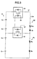
- Fig. 7 In order to detect the voltage of each of such cells, usually, the configuration shown in Fig. 7 is used. In the figure, for the sake of simplicity, only four cells are illustrated. Voltage dividing circuits P1 to P4 each of which is configured by connecting resistors RA and RB in series are connected between the output terminals of cells C1 to C4 and a ground line serving as one of common output lines, respectively. According to this configuration, the voltages of the cells C1 to C4 can be measured from voltages V1 to V4 appearing at the common junctions between the resistors RA and RB of the voltage dividing circuits P1 to P4, respectively.
- the discharging currents i1 to i4 have relationships that, as shown in Fig. 7, the discharging current i1 flows through the cell C1 only, the discharging current i2 flows through the cells C1 and C2, the discharging current i3 flows through the cells C1, C2, and C3, and so forth. Consequently, a larger current always flows through the cells C1, C2, ... which are nearer to the ground line. As a result, the capacity of each of the cells is reduced in a larger degree as the cell is nearer to the ground line.
- the capacities of the cells C1 to C4 can be leveled by charging the cell C1 the capacity of which is lowered by the largest degree, so as to be fully charged, and the other cells C2, C3, and C4 to be overcharged.
- a battery of the type in which overcharge should be avoided such as a lithium-ion battery, however, the capacities of cells cannot be leveled by the above-mentioned technique.
- the invention has been conducted under these circumstances. It is an object of the invention to provide a capacity leveling circuit for a battery group in which capacities of cells of the battery group can be leveled to enhance the reliability of the system.
- a correcting discharging circuit for discharging a cell(s) is connected between another output terminal of the battery group and the one output terminal of each of the cells, one of the voltage dividing circuits being connected to the one output terminal, the cell(s) being not connected to the one voltage dividing circuit in series.
- the leveling of the capacities of the cells can be realized by setting the amounts of discharges of the cells due to the correcting discharging circuits, and those of each of the cells due to the voltage dividing circuits to be equal to one another.
- each of the correcting discharging circuits and the voltage dividing circuits is configured by connecting a photo FET and a resistor in series.
- each of the voltage dividing circuits is configured by connecting a photo FET 1 and a resistor in series
- each of the correcting discharging circuits is configured by connecting a photo FET 2 and a resistor in series.
- Each of the photo FETs is configured by disposing light emitting and receiving diodes in the gate portion, and packaging the transistor and the diodes. Therefore, the gate terminal of the photo FET is insulated from the drain terminal, and the gate voltage is not affected by the drain voltage. In other words, even when the photo FETs have different drain voltages, all the gate voltages required for respectively driving the FETs are equal to one another, so that the on/off states of the FETs can be easily controlled.
- terminal portions of all the correcting discharging circuits which are commonly connected to the other output terminal of the battery group are formed as a single common line
- a single photo FET 2 which is commonly used by all the correcting discharging circuits is disposed in the common line
- a diode is disposed in a portion of each of the correcting discharging circuits except the common line, the diode blocking a current in a direction opposite to a current direction in a case of a turn-on of the photo FET 2, from flowing through the resistor of the correcting discharging circuit.
- the single photo FET 2 can be commonly used by all the correcting discharging circuits, and a reverse current can be prevented from flowing through the correcting discharging circuits by diodes which are more economical than a photo FET. Therefore, the production cost of the circuit can be made lower than that of a circuit in which plural photo FETs are used correspondingly with the correcting discharging circuits.
- a ratio of a resistance of each of the voltage dividing circuits to a resistance of each of the correcting discharging circuits is equal to a ratio of a number of cells of the voltage dividing circuit to a number of cells of the correcting discharging circuit, the voltage dividing circuit and the correcting discharging circuit being connected to the one output terminal of a same cell.
- the resistance ratio of a voltage dividing circuit and a correcting discharging circuit which correspond to each other is made equal to the cell number ratio of the circuits, and hence a current flowing through a cell(s) which are connected in series to the voltage dividing circuit is equal in level to that flowing through the a cell(s) which are connected in series to the correcting discharging circuit.
- the amounts of discharges of the cells can be equalized with each other simply by setting the turn-on period of the voltage dividing circuit to coincide with that of the correcting discharging circuit.
- turn-on periods of the photo FETs 1 of all the voltage dividing circuits coincide with one another.
- the on/off control of the FETs 1 can be easily performed, and the correcting discharge control for leveling the capacities by the on/off operations of the photo FET 2 of the correcting discharging circuits can be simplified.
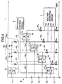
- a battery B corresponding to a battery group in the invention is configured by connecting plural cells in series.
- the negative output terminal of the battery is connected to a ground line GND.
- Voltage dividing circuits P1 to P4 each of which is configured by connecting resistors RA and RB in series are connected between the positive output terminals of cells C1 to C4 and the ground line GND, respectively.
- the resistors RA and RB are configured in the same manner so as to attain the same voltage division ratio.
- VC1 k ⁇ V1
- VC2 k ⁇ (V2 - V1)
- VC3 k ⁇ (V3 - V2)
- VC4 k ⁇ (V4 - V3)
- k is a proportional constant which depends on the voltage division ratio.
- photo FETs 11 to 14 serving as switch elements are connected between the resistor RA and the positive output terminals of the cells C1 to C4 while connecting their drain terminals to the side of the output terminals of the cells C1 to C4, respectively.
- Each of the photo FETs 11 to 14 is configured by disposing light emitting and receiving diodes in the gate portion, and packaging the transistor and the diodes. In each of the photo FETs 11 to 14, therefore, the gate terminal is insulated from the drain terminal, and the gate voltage is not affected by the drain voltage.
- the photo FETs 11 to 14 have different drain voltages, all the gate voltages required for respectively driving the FETs are standardized to a rated value (1.3 V) or the forward voltage of the light emitting diode, so that the on/off states of the FETs are easily controlled.
- the gate terminals of the photo FETs 11 to 14 are connected to a switching control circuit 5, so that the on/off states of the FETs are controlled by signals supplied from the circuit, respectively.
- the on/off control is performed in the same pattern, and at an on-duty ratio of 50% as shown in the upper right portion of Fig. 1.
- Correcting discharging circuits D1 to D3 respectively corresponding to the voltage dividing circuits P1 to P3 are connected between the positive output terminal of the battery B and the positive output terminals of the cells C1 to C3, respectively.
- Each of the correcting discharging circuits D1 to D3 is configured by connecting in series a resistor RC (one of RC1 to RC3 ⁇ serving as a current-limiting element, and a photo FET 21 serving as a switch element.
- the terminal portions which are commonly connected to the positive output terminal of the battery B are formed as a single common line
- the side opposite to the common line Lc is branched into three branch lines Lb1 to Lb3 respectively corresponding to the correcting discharging circuits D1 to D3
- the branch lines are connected to common junctions between the photo FETs 11 to 13 of the voltage dividing circuits P1 to P3 and the resistors RA, respectively.
- the single photo FET 21 which is commonly used by all the correcting discharging circuits D1 to D3 is disposed in the common line Lc.
- Sets of the resistor RC (one of RC1 to RC3) of the correcting discharging circuits D1 to D3 and a diode Di are disposed in the branch lines Lb1 to Lb3, respectively.
- the photo FET 21 is configured in the same manner as the photo FETs 11 to 14 of the aforementioned voltage dividing circuits P1 to P4.
- the gate terminal of the photo FET is connected to the switching control circuit 5.
- the switching control circuit 5 supplies to the photo FET 21 a signal which is obtained by inverting the on/off control pattern supplied to the photo FETs 11 to 14, as shown in the upper right portion of Fig. 1.
- Each of the diodes Di is connected in series to the corresponding resistor RC, in a direction along which a current opposite in direction to that flowing in the case of the turn-on of the photo FET 21 (hereinafter, such a current is referred to as "reverse current") is blocked from flowing through the resistor RC.
- reverse current a current opposite in direction to that flowing in the case of the turn-on of the photo FET 21
- the diodes Di prevent a current from flowing from the voltage dividing circuits P1 to P3 to the resistors RC.
- diodes Di may be respectively disposed in a line Ld which elongates from the common junction of the three branch lines Lb1 to Lb3 toward the two branch lines Lb2 and Lb3, and the branch line Lb3 which is branched from the line Ld, thereby preventing the reverse current from flowing through the lines.
- the diodes Di are disposed in the branch lines Lb1 to Lb3, respectively.
- expressions for strictly obtaining the values of the resistors RC1 to RC3 in consideration of the resistances of the diodes Di can be simplified as compared with those in the case of Fig. 4.
- the values of the resistors RC1 to RC3 of the correcting discharging circuits D1 to D3 are set in the following manner.
- the pairs of the voltage dividing circuit and the correcting discharging circuit P1 and D1, P2 and D2, and P3 and D3, see Figs. 2 and 3) both of which are connected to the output terminal of the same one of the cells C1 to C3, the ratio of the resistances of the circuits is equal to that of the numbers of cells which are connected in series to the respective circuits.
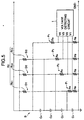
- Fig. 2 shows only the voltage dividing circuit P1 for measuring the voltage of the cell C1, and the correcting discharging circuit D1 corresponding to the voltage dividing circuit P1.
- the voltage detecting circuit 1 is activated.
- the switching control circuit 5 supplies an on/off signal of an on-duty ratio of 50% to the photo FETs 11 to 14 of all the voltage dividing circuits P1 to P4, and supplies also a signal which is obtained by inverting the on/off signal to the photo FET 21 that is common to the correcting discharging circuits D1 to D3.
- the photo FET 21 is turned off. Therefore, no current flows through the correcting discharging circuits D1 to D3 via the common line Lc.
- the potential of the terminal connected to the voltage dividing circuit P1, P2, or P3 is higher than that of the terminal on the side of the common line Lc since the photo FET 21 is turned off.
- the diodes Di which are respectively connected in series to the resistors RC prevent a current from flowing from the voltage dividing circuits P1 to P3 into the correcting discharging circuits D1 to D3. Namely, during the period when the voltages VC1 to VC4 of the cells C1 to C4 are detected, no current flows through the correcting discharging circuits D1 to D3.
- the voltage dividing circuit P1 will be described in detail with reference to Fig. 2.
- the photo FET 11 is turned on, and the photo FET 21 is turned off. Therefore, the current of the voltage dividing circuit P1 flows through the cell C1 which is connected in series to the voltage dividing circuit P1, but does not flow through the cells C2 to C4 which are not connected in series to the voltage dividing circuit P1.
- the cell C1 is made different in capacity from the other cells C2 to C4.
- the photo FET 11 When the photo FET 11 is turned off and the cell C1 is isolated from the voltage dividing circuit P1, the photo FET 21 is turned on in synchronization of the turn-off, and the cells C2 to C4 is caused to be connected to the correcting discharging circuit D1 by a parasitic diode formed in the photo FET 11. Then, a current flows through the resistor RC1 in the correcting discharging circuit D1 based on the electromotive forces VC2 to VC4 of the cells C2 to C4, and the cells C2 to C4 are discharged. At this time, the current of the correcting discharging circuit D1 does not flow through the cell C1, and hence the cell C1 is not discharged.
- the resistance ratio is equal to the cell number ratio
- the current flowing through the cell C1 which is connected in series to the voltage dividing circuit P1 is equal in level to that flowing through the cells C2 to C4 which are connected in series to the correcting discharging circuit D1.
- the turn-on periods of the photo FETs 11 and 21 are the same time period. Therefore, currents of the same level respectively flow through the voltage dividing circuit P1 and the correcting discharging circuit D1 for the same time period, so that the amounts of discharge of the cells C1 to C4 are equal to one another, whereby the capacities of the cells can be leveled.
- the capacities can be leveled among the cells C1 and C2 which are connected in series to the voltage dividing circuit P2 and the other cells C3 and C4, and among the cells C1, C2, and C3 which are connected in series to the voltage dividing circuit P3 and the other cell C4.
- the voltage detecting circuit 1 detects the voltage of the cell C1 to be 0 volt. As a result of the detection of 0 volt, it is possible to detect the occurrence of the breakage of the line.
- the amount of discharges of each of the cells due to the correcting discharging circuits D1 to D3 is set to be equal to that of each of the cells due to the voltage dividing circuits P1 to P3, and hence the leveling of the capacities of the cells can be realized.
- the differences among the amounts of discharges of the cells C1 to C4 due to the voltage dividing circuits P1 to P3 are compensated with discharges due to the correcting discharging circuits D1 to D3, whereby capacity variations among the cells which are mainly caused by discharges through the voltage dividing circuits can be prevented from occurring. Consequently, it is possible to attain an effect that capacity variations among the cells which are produced by another cause such as deterioration can be surely detected.
- the turn-on periods of the photo FETs 11 to 14 of all the voltage dividing circuits P1 to P4 are set to be equal to each other, all the FETs can be operated by a common on/off signal, so that the on/off control of the FETs can be easily performed. Since the turn-on periods of the correcting discharging circuits D1 to D3 coincide with those of the voltage dividing circuits P1 to P4, the on/off control can be further easily performed.
- the single photo FET 21 is commonly used by all the correcting discharging circuits D1 to D3, and a reverse current is prevented from flowing through the correcting discharging circuits D1 to D3 by the diodes Di which are more economical than a photo FET. Therefore, the production cost of the circuit can be made lower than that of a circuit in which plural photo FETs are used correspondingly with the correcting discharging circuits D1 to D3.
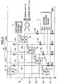
- Fig. 6 shows a second embodiment in which the signals supplied from the switching control circuit to the photo FETs are configured differently from those in the first embodiment.
- each of the correcting discharging circuits is not provided with a diode.
- the other configuration is identical with that of the first embodiment. Therefore, the identical components are denoted by the same reference numerals, and duplicated description is omitted.
- the switching control circuit 5A in the embodiment supplies the same signal (for example, the on/off signal of an on-duty ratio of 50%) as that supplied to the photo FETs 11 to 14 of the voltage dividing circuits P1 to P4, to the photo FET 21 of the correcting discharging circuits D1 to D3.
- the same signal for example, the on/off signal of an on-duty ratio of 50%
- the leveling of the capacities of the cells can be realized in the same manner as the first embodiment, and diodes are not required to be disposed, while the photo FET 21 is commonly used by the correcting discharging circuits D1 to D3.
Applications Claiming Priority (4)
| Application Number | Priority Date | Filing Date | Title |
|---|---|---|---|
| JP8650699 | 1999-03-29 | ||
| JP8650699 | 1999-03-29 | ||
| JP29800199A JP4022797B2 (ja) | 1999-03-29 | 1999-10-20 | 群電池の容量平準化回路 |
| JP29800199 | 1999-10-20 |
Publications (2)
| Publication Number | Publication Date |
|---|---|
| EP1041694A2 true EP1041694A2 (fr) | 2000-10-04 |
| EP1041694A3 EP1041694A3 (fr) | 2001-03-21 |
Family
ID=26427610
Family Applications (1)
| Application Number | Title | Priority Date | Filing Date |
|---|---|---|---|
| EP00106639A Withdrawn EP1041694A3 (fr) | 1999-03-29 | 2000-03-28 | Circuit d'egalisation de capacité pour un groupe de batteries |
Country Status (3)
| Country | Link |
|---|---|
| US (1) | US6191555B1 (fr) |
| EP (1) | EP1041694A3 (fr) |
| JP (1) | JP4022797B2 (fr) |
Cited By (2)
| Publication number | Priority date | Publication date | Assignee | Title |
|---|---|---|---|---|
| US6340889B1 (en) * | 1999-04-08 | 2002-01-22 | Seiko Instruments Inc. | Battery state monitoring circuit and battery apparatus |
| US6429623B2 (en) | 2000-04-05 | 2002-08-06 | Asahi Kogaku Kogyo Kabushiki Kaisha | Power-supply unit incorporating an electric double layer capacitor, and a method of charging the electric double layer capacitor |
Families Citing this family (9)
| Publication number | Priority date | Publication date | Assignee | Title |
|---|---|---|---|---|
| US6678132B1 (en) * | 2002-09-06 | 2004-01-13 | Bae Systems Controls, Inc. | Ground fault detection system |
| CN101682091B (zh) * | 2007-06-08 | 2012-07-25 | 松下电器产业株式会社 | 电源系统及组电池的控制方法 |
| JP2009072039A (ja) * | 2007-09-18 | 2009-04-02 | Panasonic Corp | 電源システム |
| DE102007049528B4 (de) * | 2007-10-15 | 2009-06-25 | Panasonic Electronic Devices Europe Gmbh | Verfahren und Vorrichtung zur Messung von Zellenspannungen in einer Mehrzahl von in Reihe geschalteten Akkumulatorzellen |
| JP2010009796A (ja) * | 2008-06-25 | 2010-01-14 | Nec Tokin Corp | 二次電池パック |
| JP2009103706A (ja) * | 2008-12-05 | 2009-05-14 | Shin Kobe Electric Mach Co Ltd | 電池電圧検出線の検査方法、検査回路及び電池モジュール |
| CN106786944B (zh) * | 2016-12-31 | 2020-12-18 | 华为技术有限公司 | 一种串联电池组单体电池的采样电路、均衡电路及系统 |
| KR102236384B1 (ko) | 2017-10-27 | 2021-04-05 | 주식회사 엘지화학 | 배터리 밸런싱을 위한 장치 및 그것을 포함하는 배터리팩 |
| JP7073904B2 (ja) | 2018-05-21 | 2022-05-24 | 株式会社Gsユアサ | 蓄電装置、外部放電装置、及び、蓄電装置の外部放電装置による放電方法 |
Citations (2)
| Publication number | Priority date | Publication date | Assignee | Title |
|---|---|---|---|---|
| US5258244A (en) * | 1991-12-09 | 1993-11-02 | Hughes Aircraft Company | Reversible automatic cell bypass circuit |
| US5841265A (en) * | 1992-11-24 | 1998-11-24 | Seiko Instruments Inc. | Charge/discharge control circuit and chargeable electric power source apparatus |
Family Cites Families (5)
| Publication number | Priority date | Publication date | Assignee | Title |
|---|---|---|---|---|
| US5206578A (en) * | 1991-10-15 | 1993-04-27 | Norvik Technologies Inc. | Monitoring system for batteries during charge and discharge |
| DE4422409C2 (de) * | 1994-06-29 | 1996-07-11 | Fraunhofer Ges Forschung | Vorrichtung zum Ladungsaustausch zwischen einer Vielzahl von in Reihe geschalteten Energiespeichern oder -wandlern |
| US5710504A (en) * | 1996-05-20 | 1998-01-20 | The Board Of Trustees Of The University Of Illinois | Switched capacitor system for automatic battery equalization |
| US5773958A (en) * | 1997-01-03 | 1998-06-30 | Ovonic Battery Company, Inc. | Apparatus for detecting cell reversal in rechargeable batteries |
| US5898291A (en) * | 1998-01-26 | 1999-04-27 | Space Systems/Loral, Inc. | Battery cell bypass topology |
-
1999
- 1999-10-20 JP JP29800199A patent/JP4022797B2/ja not_active Expired - Fee Related
-
2000
- 2000-03-28 EP EP00106639A patent/EP1041694A3/fr not_active Withdrawn
- 2000-03-29 US US09/538,287 patent/US6191555B1/en not_active Expired - Fee Related
Patent Citations (2)
| Publication number | Priority date | Publication date | Assignee | Title |
|---|---|---|---|---|
| US5258244A (en) * | 1991-12-09 | 1993-11-02 | Hughes Aircraft Company | Reversible automatic cell bypass circuit |
| US5841265A (en) * | 1992-11-24 | 1998-11-24 | Seiko Instruments Inc. | Charge/discharge control circuit and chargeable electric power source apparatus |
Cited By (2)
| Publication number | Priority date | Publication date | Assignee | Title |
|---|---|---|---|---|
| US6340889B1 (en) * | 1999-04-08 | 2002-01-22 | Seiko Instruments Inc. | Battery state monitoring circuit and battery apparatus |
| US6429623B2 (en) | 2000-04-05 | 2002-08-06 | Asahi Kogaku Kogyo Kabushiki Kaisha | Power-supply unit incorporating an electric double layer capacitor, and a method of charging the electric double layer capacitor |
Also Published As
| Publication number | Publication date |
|---|---|
| JP2000350375A (ja) | 2000-12-15 |
| US6191555B1 (en) | 2001-02-20 |
| EP1041694A3 (fr) | 2001-03-21 |
| JP4022797B2 (ja) | 2007-12-19 |
Similar Documents
| Publication | Publication Date | Title |
|---|---|---|
| US6169385B1 (en) | Capacity leveling circuit for a battery group | |
| KR101208874B1 (ko) | 팩 전지 | |
| US6181108B1 (en) | Overcharge/overdischarge detecting circuit having current detecting means with latch function and chargeable electric power source apparatus | |
| KR101444962B1 (ko) | 배터리 팩에서의 셀들을 모니터링하고 밸런싱하는 방법 및 시스템 | |
| US8487590B2 (en) | Cell controller having a unit cell voltage detecting section | |
| JP4326415B2 (ja) | 車両用の電源装置 | |
| JP4381239B2 (ja) | 車両用の電源装置 | |
| JP4583219B2 (ja) | 車両用の電源装置 | |
| JP4836729B2 (ja) | 車両用の電源装置とこの電源装置の断線検出方法 | |
| KR101727748B1 (ko) | 배터리의 보호 회로 장치 | |
| US20080100266A1 (en) | Semiconductor integrated circuit device | |
| EP1041694A2 (fr) | Circuit d'egalisation de capacité pour un groupe de batteries | |
| JP2006149068A (ja) | 組電池管理装置 | |
| CN103296715A (zh) | 开关故障诊断装置、电池组以及开关故障诊断程序、开关故障诊断方法 | |
| KR20090004745A (ko) | 배터리 상태 감시 회로 및 배터리 장치 | |
| US20090295329A1 (en) | Vehicle power supply device | |
| US20120001640A1 (en) | Power supply device capable of detecting disconnection of ground line | |
| US10215810B2 (en) | Battery monitoring system | |
| KR101773053B1 (ko) | 전지 감시 유닛 | |
| KR19990013384A (ko) | 재충전가능한 바테리 셀의 충전 및 방전을 제어하는데 적합한양방향 전류 제어 회로 | |
| EP1146345B1 (fr) | Appareil de mesure pour la tension multiplexée | |
| US9575134B2 (en) | Assembled-battery voltage detection device | |
| US6225779B1 (en) | Power supply monitoring integrated circuit device for individually monitoring voltages of cells | |
| US20040196007A1 (en) | Battery pack malfunction detection apparatus and battery pack malfunction detection method | |
| JP5219653B2 (ja) | 電源装置 |
Legal Events
| Date | Code | Title | Description |
|---|---|---|---|
| PUAI | Public reference made under article 153(3) epc to a published international application that has entered the european phase |
Free format text: ORIGINAL CODE: 0009012 |
|
| AK | Designated contracting states |
Kind code of ref document: A2 Designated state(s): DE FR Kind code of ref document: A2 Designated state(s): AT BE CH CY DE DK ES FI FR GB GR IE IT LI LU MC NL PT SE |
|
| AX | Request for extension of the european patent |
Free format text: AL;LT;LV;MK;RO;SI |
|
| PUAL | Search report despatched |
Free format text: ORIGINAL CODE: 0009013 |
|
| AK | Designated contracting states |
Kind code of ref document: A3 Designated state(s): AT BE CH CY DE DK ES FI FR GB GR IE IT LI LU MC NL PT SE |
|
| AX | Request for extension of the european patent |
Free format text: AL;LT;LV;MK;RO;SI |
|
| 17P | Request for examination filed |
Effective date: 20010718 |
|
| AKX | Designation fees paid |
Free format text: DE FR |
|
| RAP1 | Party data changed (applicant data changed or rights of an application transferred) |
Owner name: GS YUASA CORPORATION |
|
| STAA | Information on the status of an ep patent application or granted ep patent |
Free format text: STATUS: THE APPLICATION HAS BEEN WITHDRAWN |
|
| 18W | Application withdrawn |
Effective date: 20070530 |